SUMMARY SoC has driven the evolution of embedded systems or con-sumer electronics. Multi-core/multi-IP is the key technology to integrate many functions on a SoC for future embedded applications. In this paper, the transition of SoC and its required functions for cellular phones as an example is described. And the state-of-the-art multi-core technology of homogeneous type and heterogeneous type are shown. When many cores and IPs are integrated on a chip, collaboration between cores and IPs be-comes important to meet requirement. To realize it, “MPSoC Platform” concept and elementary technology for this platform is described.
key words: SoC, multi-core, embedded system, platform
1. Introduction
Consumer electronics, such as cellular phone, car informa-tion system, and digital TV, have evolved, which are driven by digitalization and networking. These consumer electron-ics require heavy digital processing for video, network or rich graphical interface. SoC (System-on-a-Chip), which executes these functions, is a key device to support evolu-tion of consumer electronics.
CMOS scaling to nano-meter era enables tens of func-tions to be integrated on a chip, so that recent SoC has mul-tiple CPU cores and mulmul-tiple IPs (Intellectual Property) to support unlimited requirements from end-users of consumer electronics.
In this paper, transition of SoC for cellular phones are described to introduce what kind of functions or IPs are required to be integrated on a chip. Then, state-of-the-art multi-core technology of homogeneous type and heteroge-neous type is described. And MPSoC platform to control multi-core/multi-IP to meet “non-functional requirement” also described for further evolution of SoCs.
2. Multi-Core/Multi-IP Technology for Embedded Ap-plications
2.1 Transition and State-of-the-Art of SoC
The evolution of consumer electronics is very rapid. Espe-cially, cellular phone has become not only communication tool, but also multimedia terminal with integrated digital-TV, digital still camera, portable game, GPS navigation
sys-Manuscript received March 12, 2009.
†The author is with Hitachi, Ltd., Kokubunji-shi, 185-8601
Japan.
††The author is with Renesas Technology Corp., Kodaira-shi,
187-8588 Japan.
a) E-mail: [email protected] DOI: 10.1587/transele.E92.C.1232
Fig. 1 Transition of SoC for cellular phones.
tem and so on.
To support evolution of cellular phone, the SoC is re-quired to have much performance with low power. Figure 1 shows transition of application processor in cellular phone, which supports many functions integration and acceleration shown in [1]–[3]. The first generation of application proces-sor [1], which was fabricated with 180 nm technology, only has a RISC CPU core with DSP and a few peripheral IPs for I/O such as serial interface and IC card interfaces. Many of functions are executed by software with help of DSP and relatively huge SRAM.
The second generation of application processor [2], which fabricated by 130 nm technology, integrates not only enhanced CPU core but also several multimedia ator such as MPEG-2 accelerator, 3D graphics acceler-ator and Java acceleracceler-ator. In the enhanced CPU core, micro-architecture level low-power technology, such as fine-grained gated clock and pointer pipeline scheme, is adopted and realized 4.5GIPS/W with 216 MHz performance using low-leakage 130 nm process. Multimedia accelerators are good solution to meet users requirements with limited power consumption. For example, Java accelerator is integrated this application processor. It translates Java bytecodes to native CPU instruction dynamically. Thus overhead cycles for interpretation of bytecodes by software can be removed and it can achieve about 10 times faster performance with-out additional power consumption [4].
The second generation of application processor has 5 power domains using on-chip power switches and partial power gating scheme is implemented [2]. According to the operation mode of cellular phone, Ultra Standby mode or Resume Standby mode is used for longer battery life. In
tra Standby mode, almost circuit block is power-gated ex-cept I/O block and blocks for wake-up. In Resume Standby mode, backup latch and URAM (User RAM) is turned on for quick restart.
The third generation of application processor [3] inte-grated not only multimedia functions of cellular phone, but also digital baseband functions of W-CDMA and GSM. This means whole digital functions of cellular phone can be in-tegrated in one SoC. To realize it, this SoC has three CPUs cores, several DSPs and enhanced multimedia accelerators.
2.2 Multi-Core Architecture for Embedded Applications
Described the section above, many functions are integrated in a SoC. These functions require dedicated CPUs and IPs. Multi-core/Multi-IP technology is used for this purpose. On the other hand, each function such as image processing or recognition requires more and more performance as shown in Fig. 2. But operating frequency of CPU becomes difficult to achieve over GHz, because of increasing power consump-tion. Therefore, multi-core is used to accelerate a certain function by parallel processing.
To fulfill the requirements above, we have developed multi-core architecture, which has features below.
(1) Multi-core architecture which supports both SMP (Symmetric Multi-Processing) and AMP (Asymmet-ric Multi-Processing)
(2) Heterogeneous multi-core which supports not only general CPU core but also dynamic reconfigurable processor
2.2.1 Multi-Core Architecture for Both SMP and AMP Support
Multi-core technology has mainly used in general purpose processors for PC or servers so far. And SMP model, which a main memory is shared by each processor and cache co-herency mechanism is supported by hardware, is used for general purpose processors. This SMP model suitable to de-velop software because of transparency of distributed mem-ory (= cache). To adapt SMP model to embedded proces-sors is useful to share programming model with PC industry, that means productivity or portability of programs becomes higher.
Fig. 3 Block diagram of mullti-core processor.
But as described previous session, multi-core technol-ogy is used for integration of multi functions in embedded SoCs. In this case, the possibility of data sharing between processors is relatively low and the performance overhead of cache coherency should be negligible. Local memory ar-chitecture, which programmers themselves control data lo-cation and transfer on a LSI, is also used in embedded SoCs for performance optimization especially targeting real-time applications. Thus, both SMP and AMP mode are required for wide range of applications and programmers.
Figure 3 shows the block diagram of multi-core based on SuperH(SH) architecture, which supports both SMP and AMP [5]. Up to 4 cores are connected by a snoop controller to maintain cache coherency. And in the snoop controller, arbitral cores are designated whether the core is involved cache coherency or not. Each core has local memories of ILRAM (Instruction Local RAM), OLRAM (Operand Lo-cal RAM) and URAM (User RAM). ILRAM and OLRAM are relatively small and can be accessed in one cycle from each CPU. URAM is shared by instructions and operand and accessed in two cycles. These local memory is mapped both local space for each core and shared space from all cores in whole address space. The local memory can be used not only by CPU cores but also DMAC and DTU (Data Trans-fer Unit). DTU is dedicated DMAC in CPU core to support higher programmability.
The SMP/AMP mechanism affects low-power mode of each CPU. Each CPU has four low-power modes. As usual, sleep mode and power-down mode (U-standby mode) are supported. Additionally, CPU has light sleep mode and R-standby mode. In the light sleep mode, clock for CPU is gated, but clock for caches is not gated. This is because cache should be active to join the cache coherency mecha-nism. For example, if the cache in the light sleep mode has a dirty line, it should flash out to other CPU when the line is accessed by the CPU. In the R-standby mode, the power of CPU and cache is gated, but power of local memories is kept to be turned on. This is because local memories can keep its contents without backup to main memory. It helps to move into R-standby mode with less performance overhead.
The die photograph of prototype multi-core SoC is shown in Fig. 4 [6]. This prototype SoC is fabricated 90 nm process technology and obtained 4320 MIPS (measured by
Fig. 4 Die photograph of multi-core protoype.
Fig. 5 Level of parallelism and suitable architecture.
Dhrystone 2.1) and 16.8 GFLOPS by 600 MHz quad CPU cores.
2.2.2 Heterogeneous Multi-Core
Exploiting parallelism is essential to obtain good perfor-mance and power efficiency. There are several levels of par-allelism such as instruction level, data level, task level and so on. And the characteristic of parallelism require differ-ent type of architecture as shown in Fig. 5. In particular, multimedia applications have various types of data paral-lelism, so that homogenous multi-core is not enough to use them and it causes insufficient performance or energy effi-ciency. Conventionally, hardwired IPs are used in this area, but various multimedia standards appear frequently and de-sign and mask cost becomes too huge, so that more flexible solution will be required in the future. Thus, heterogeneous multi-core, which has combination of multi-core of embed-ded CPU cores and dynamic reconfigurable processors, is proposed.
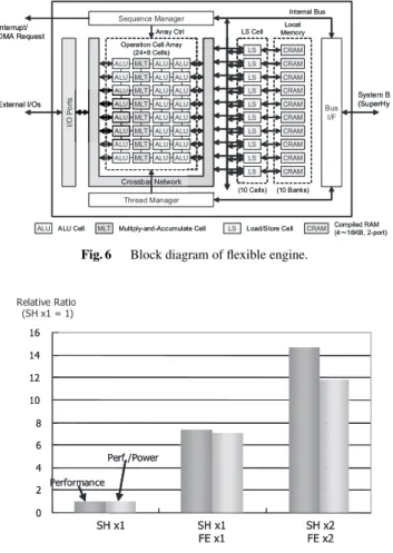
As one of dynamic reconfigurable processors, Flexible Engine (FE) is proposed [7]. As shown in Fig. 6, FE con-sists of 24 ALUs and 8 MLTs (Multiplier) cells connected by 2D mesh each other, 10 CRAMs controlled by load-store (LS) cells, and crossbar network between 10 CRAMs and the ALU/MLT array. An operation of each ALU/MLT cells or LS cells is stored in register in the each cell. A set of op-erations in each cells is called configuration plane. Once a configuration plane is set to each cell, data is read out from
Fig. 6 Block diagram of flexible engine.
Fig. 7 Performance and energy efficiency of heterogeneous multi-core.
CRAMs, processed by the ALU/MLT array and stored to CRAMs automatically. After execution of the configuration plane is completed, the next configuration plane is set from the internal cache of configuration planes, and data is pro-cessed continuously. The FE can execute without fetching and decoding operations, so that it can get good energy effi-ciency. Using 90 nm process, FE can achieve 91.4 GOPS/W with 300 MHz operating frequency.
The performance and energy efficiency is shown in Fig. 7 using AAC encoding program as a multimedia bench-mark [8]. Among in the AAC program, filter bank and quan-tization routine are executed by a FE and the other routine such as preprocessing, Huffman coding and bit stream gen-eration are executed by a CPU core. Data transfer between CPU core and FE, DTU is used to get high data through-put by long burst data transfer. Using 2 CPU cores (SH) and 2 FEs, about 14 times faster performance and 12 times higher energy efficiency can be achieved comparing with single CPU core.
3. “MPSoC Platform” for Multi-Core
As described section above, many processor cores and IPs are integrated onto one SoC in these years. These proces-sors and IPs are required to collaborate each other in order to implement several functions. Conventionally, the
num-Fig. 8 Concept of MPSoC platform.
ber of implemented functions on a chip is only a few, but in future this number will be several dozen. In this case, to meet “non-functional requirement” becomes severe prob-lem when several dozen of functions are executed with-out knowledge of other function’s status. The term “non-functional requirement” here is specification of quality of SoC such as power consumption, realtime constraint, reli-ability and so on, rather than specification of behavior of SoC. This term is used for IT systems which becomes more large-scaled and complex. Similarly, complicated SoCs are also required to define and implement non-functional re-quirement. “MPSoC Platform,” which is a mechanism or a scheme to collaborate multiple processor cores and IPs, is proposed in this paper to solve this problem.
C. Moore, AMD Fellow, described four generation of multi-core processor below in [9].
• Gen-0: Hasty integration of a bunch of cores
• Gen-1: Balanced integration of cores and system func-tionality
• Gen-2: Chip-level framework & infrastructure to support range of CMP (Chip Multi-Processor) variants
• Gen-3: Runtime adaptive flexibility and Introspective self-management
From this aspect, the “MPSoC Platform” realizes Gen-2 and Gen-3.
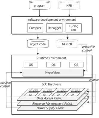
Figure 8 shows the outline drawing of MPSoC plat-form. Generally, functional requirement is given by pro-grams and translated to object codes using a software devel-opment environment which include compilers and debugger. The object code is passed to a runtime environment, which include SoC hardware, operating systems (OS) and runtime
Fig. 9 Power supply fabric.
libraries.
On the other hand, the non-functional requirement is conventionally defined by documents, evaluated by simu-lation or actual systems with typical programs, and im-plemented by tuning of object codes. In future, the non-functional requirement is defined more explicit way and translated to “NFR code” via a software development envi-ronment. This NFR code controls SoC hardware with sup-port of a runtime environment or “Hypervisor.” To maintain SoC hardware, OS is used conventionally. But OS is bun-dled to a certain function (e.g. a multimedia function uses a realtime OS and a user interface function uses a general OS), so that “Hypervisor” placed under OS will be required, in order to control SoC hardware primitively and to execute “NFR code.” The “Hypervisor” gets “NFR codes” when SoC is booted or a program is invoked, and it controls SoC hardware proactively. Also, it gets dynamic status of SoC and control SoC hardware reactively. Cooperation of proac-tive control and reacproac-tive control realizes non-functional re-quirement such as power consumption, realtime operation and reliability.
Hardware mechanism to implement non-functional re-quirement is also required. In this paper, interconnect mech-anism for each processor cores and IPs with hardware NFR control is called “fabric.” There are several types of fabrics according to its purpose. For example, to control power con-sumption, power supply fabric on a chip is required. Sim-ilarly, resource management fabric and data access fabric are required to manage shared resource on a chip and to pro-tect data for high reliability, respectively.
Current research activities for MPSoC Platform are shown in the following section.
3.1 Platform for Power Consumption Control
The power consumption becomes major issue. Especially, reducing leakage current is important after sub-100 nm pro-cess era. Several circuit techniques are proposed to reduce leakage current, and power-gating is well used since it is used by embedded SoC for cellular phones [2].
An example of power supply fabric (PSF) is proposed in [10] (Fig. 9). Over 20 power domains are defined for
in-Fig. 10 Power domain of multi-core processor.
dividual power-gating. Each power domain includes a few CPU cores or IPs, and it is separated by N-MOS power switches. The power switches are controlled by power switch controller (PSWC) for slew rate control to reduce noise. The PSF also supports long signal communication between power domains and automatic status backup using CPD (Common Power Domain). A CPD can be placed in each power domain and remains tuned-on while the power domain is turned-off.
There are several ways of PSWC control from soft-ware. The [3] shows power domain control for a cellular phone system according to use cases, such as Stand-by, W-CDMA paging, TV telephony and so on.
Other control scheme that is compiler generates power domain control code is proposed in [11]. The target SoC has 17 power domains, which consist of 8 domains for CPU cores, 8 domains for User-RAMs and 1 control do-main shown in Fig. 10. The proposed compiler generates parallelized and scheduled codes for each CPU core. The compiler can know idle period of each CPU core when it waits for data from the other CPU. And the compiler can insert power shutdown code for the CPU core when it en-ters the idle period. The power shutdown code is accepted by “Hypervisor” and controls the PSWC. When this control is adopted to AAC encode program using 8 CPU cores in parallel, 86% of leakage current can be reduced.
3.2 Platform for Data Access Control
As described in Sect. 2, it becomes common that multiple functions are integrated into a SoC and share main memory. In this case, each function should not be disturbed by other functions. But if a program of a certain function get mal-functioned cased by bugs or viruses, a non-intentional mem-ory access occurs and other function get malfunctioned also. This situation will be a serious problem when functions with different reliability level are integrated on a same SoC. Con-sidering a future car navigation system, for example, com-munication function to internet and support function of ve-hicle dynamics control are integrated with basic function of location system by GPS (Global Positioning System) for
Fig. 11 Domain isolation.
Fig. 12 Data access fabric for domain isolation.
navigation (shown in Fig. 11). In this case, if the communi-cation function is malfunctioned by a virus from the internet and it affects the vehicle dynamics control, then safety of the vehicle may be threatened. Thus, the access control scheme of each functional domain is proposed that means each func-tional domain is isolated by observing every access to shared memory or resources.
In general, processor cores and IPs are connected by on-chip system bus, and the data access fabric for functional domain isolation has Logical Partition Controller (LPC) in order to observe the data access to shared recourses shown in Fig. 12 [12]. In the LPC, there is a table which indicates whether a CPU or IP can access a certain shared resource (e.g. shared memory area, I/O space) or not. Every data access including I/O access is checked by LPC using this table. For example, memory area0 can be accessed by CPU0 only and access from CPU1 is prohibited. HDD interface can be access by CPU1 only, and CPU0 cannot access the HDD interface. The table in LPC is loaded when this SoC is powered-on and locked during operation mode.
When each CPU core or IP accesses to shared mem-ory or I/Os, every bus transaction goes through LPC and is checked. If the access violation is detected, the information of violation is propagated to “Hypervisor.” The “Hypervi-sor” responds properly according to the propagated infor-mation. For example, if a certain CPU accesses prohibited area frequently, Hypervisor forces to shutdown and restart
Fig. 13 Block diagram of resource management fabric.
the OS on the CPU.
Conventionally, an isolation mechanism between func-tions is implemented by a virtual machine for general pur-pose processors. But it is not suitable for embedded SoCs because of performance overhead. Thus, the hardware sup-port of isolation done by data access fabric is necessary. The experimental result shows only 5% of performance overhead in almost programs in lmbench benchmark.
3.3 Platform for Shared Resource Management
When many functions integrated on a SoC are executed independently or “selfishly,” conflict of shared resources should be problem. For example, to access external memory from several functions, a certain function dominates mem-ory bandwidth and other functions are disturbed that means these functions cannot meet non-functional requirement of realtime specification. Power consumption or thermal bud-get of a SoC also has limitation, and if most of functions are executed without the budget, power consumption con-trol may be collapsed in the worst case. In future, the num-ber of functions on a SoC will be increased. It makes wider difference between a typical case and the worst case, and it causes upper limit of the number of functions using conven-tional design methodology which guarantee the worst case specification. To solve this problem, the shared resource management technique is proposed.
Figure 13 shows the hardware configuration including
resource management fabric to implement shared resource
management [13]. The target shared resource is thermal budget of the SoC. Conceptually, the resource management fabric consist of (1) monitor of each function, (2) monitor of status of shared resource, and (3) controller to calculate and distribute budget of each function. To control thermal bud-get, the resource management fabric has (1) performance monitor to check the execution status, (2) thermal sensors to measure temperature of the SoC, and (3) dedicated mi-crocontroller core called Resource Management Controller (RMC).
The monitored information from performance moni-tors and thermal sensors is propagated to RMC. In the RMC, projected temperature is calculated using current chip tem-perature and current power consumption of each CPU with
Fig. 14 Effect of thermal control.
Fig. 15 Die photograph of prototype of SoC with resource management fabric.
information of its performance monitor. If projected tem-perature will exceed a certain threshold, the RMC calcu-lates target power consumption for each CPU and controls the operating frequency of each CPU to reduce power con-sumption.
Figure 14 shows the simulation result of thermal con-trol. The upper graph shows temperature of the SoC and am-bient temperature assumed from 40◦C to 70◦C. In this case, if there are no thermal control, leakage current is increased and chip temperature exceed 85◦C, which is thermal bud-get of this SoC. When this resource management scheme is used, the RMC controls the operating frequency reactively, and the operating frequency of CPUs is dropped gradually as shown in lower graph. Then chip temperature can be kept under 85◦C.
This mechanism is implemented on a SoC, which has 2 CPU cores and 2 HW-IPs as shown in Fig. 15. The RMC and thermal sensors are integrated on the same SoC. The area overhead of this mechanism is small. The RMC core and peripheral occupies 0.4 mm2 and thermal sensor occupies
0.3 mm2 using 90 nm CMOS process. We confirmed the RMC can control the operating frequency of each CPU core dynamically depending on the ambient temperature when a MPEG-2 decoder program is executed on each CPU core.
4. Future Direction
In the future, CMOS scaling and 3D integration technology will drive more integration of processor cores and IPs.
Es-opment environment would be the key to get good optimiza-tion of whole SoC. Runtime environment with “Hypervisor” should be co-developed with hardware mechanism which is called “fabric” in this paper. That means standardiza-tion of “non-funcstandardiza-tional requirement” definistandardiza-tion and collab-oration between SoC vendors, tool-chain vendors and con-sumer electronics vendors will be needed.
5. Conclusion
Considering evolution of SoC for embedded applications, multi-core/multi-IP technology will be the key technology to support integration of many functions on a chip and get enough performance for each function. To integrate many functions on a chip, flexibility of multi-core configuration and memory model is required. Thus, multi-core architec-ture, which both SMP and AMP are supported, is proposed. To get enough performance for each function, exploiting parallelism from each function is important. Thus, heteroge-neous multi-core architecture is proposed, which uses both embedded CPU cores and dynamic reconfigurable proces-sors. As a dynamic reconfigurable processor, Flexible En-gine, which consists of 32 ALUs and 10 CRAMs, is pro-posed. Combination of CPU core and Flexible Engine can achieve about 12 times higher energy efficiency than single CPU core.
In the future, many functions are integrated into a SoC and to meet “non-functional requirement” becomes diffi-cult because of “selfish” execution of each function. To optimize chip level with collaboration between functions, “MPSoC Platform” to connect many cores and IPs intelli-gently is required. To meet “non-functional requirement” of power consumption, reliability and thermal budget, current research activity for “MPSoC platform” and experimental results are shown.
Acknowledgments
The authors would like to acknowledge Prof. Kasahara of Waseda University, Prof. Kuroda of Keio Univer-sity, A. Hasegawa, O. Nishii of Renesas Technology, K. Uchiyama, H. Mizuno, K. Osada, T. Nojiri and col-leagues of Hitachi CRL.
The part of this work related to [6] and [11] was supported by NEDO (New Energy and Industrial Technol-ogy Development Organization) P03022, a joint project of Waseda University, Renesas Technology Corp., and Hitachi Ltd.
mains in 90-nm low-power multi-CPU processor,” ISSCC Digest of Technical Papers, pp.74–75, Feb. 2006.
[4] T. Yamada, et al., “A hardware accelerator for JavaTMplatforms on a 130-nm embedded processor core,” IEICE Trans. Electron., vol.E90-C, no.2, pp.523–530, Feb. 2007.
[5] T. Kamei, “SH-X3: Enhanced SuperH core for low-power multi-processor systems,” Micromulti-processor Forum 2006.
[6] Y. Yoshida, et al., “A 4320 MIPS four-processor core SMP/AMP with individually managed clock frequency for low power consump-tion,” ISSCC Digest of Technical Papers, pp.100–101, Feb. 2007. [7] T. Kodama, et al., “Flexible engine: A dynamic reconfigurable
ac-celerator with high performance and low power consumption,” Proc. IEEE Symposium on Low-Power and High-Speed Chips (COOL Chips IX), 2006.
[8] M. Ito, et al., “Heterogeneous multiprocessor on a chip which en-ables 54x AAC-LC stereo encoding,” VLSI Sympo. 2007. [9] C. Moore, “Chip multi-processors: Now and into the future,” Panel
Discussion, ICCD 2005.
[10] Y. Kanno, et al., “Hierarchical power distribution with 20 power do-mains in 90-nm low-power multi-CPU processor,” ISSCC 2006. [11] M. Ito, et al., “An 8640 MIPS SoC with independent power-off
con-trol of 8 CPUs and 8 RAMs by an automatic parallelizing compiler,” ISSCC Digest of Technical Papers, pp.90–91, Feb. 2008.
[12] A. Takahashi, et al., “Domain isolation technique for multi-core LSI,” FIT2008.
[13] M. Saen, et al., “Embedded SoC resource manager to control tem-perature and data bandwidth,” ISSCC 2007.
[14] K. Niitsu, et al., “An inductive-coupling link for 3D integration of a 90 nm CMOS processor and a 65 nm CMOS SRAM,” ISSCC09, 2009.
Naohiko Irie received B.E. degree in electri-cal engineering and M.E. degree in information system from the Kyushu University, Japan, in 1988 and 1990, respectively. He joined the Cen-tral Research Laboratory, Hitachi, Ltd., Tokyo, Japan, in 1990. He had worked on computer ar-chitecture and micro-arar-chitecture of mainframe, SMP server after he joined Hitachi. Since 1998, he has worked on architecture for embedded processor and SoC, such as SH-Mobile for cel-lular phones, and led multi-core SoC project with Renesas Technology. He was a visiting professor of Kyushu Uni-versity from 2007 to 2009. He was awarded Best Paper Award for Young Researcher of IPSJ National Convention and IPSJ Best Paper Award, in 1989 and 1991, respectively. He is a member of IPSJ.
Semiconductor Integrated Circuits Division in Hitachi Ltd. in 1995. He moved to Renesas Technology Corp. in 2003. He was belonging to SuperH (Japan), Ltd. from 2001 to 2004 to conduct SH processor licensing and development. He is currently working with Renesas Technology conduct-ing CPU core design, SH-mobile design and Multi-media Soc design. He had headed the SH-Mobile G series project to design low-power and high-performance LSI’s. He is the department manager of Mobile SOC design department at Renesas. He is a member of IEEE (SSCS), ACM, and IPSJ.