A D C
Section 16. Analog-to-Digital Converter (ADC)
HIGHLIGHTS
This section of the manual contains the following major topics:
16.1 Introduction ... 16-2
16.2 Control Registers ... 16-4
16.3 A/D Terminology and Conversion Sequence ... 16-14
16.4 ADC Module Configuration ... 16-16
16.5 Selecting the Voltage Reference Source ... 16-16
16.6 Selecting the A/D Conversion Clock ... 16-17
16.7 Selecting Analog Inputs for Sampling ... 16-18
16.8 Enabling the Module ... 16-20
16.9 Specifying Sample/Conversion Control ... 16-20
16.10 How to Start Sampling ... 16-21
16.11 How to Stop Sampling and Start Conversions ... 16-22
16.12 Controlling Sample/Conversion Operation... 16-32
16.13 Specifying Conversion Results Buffering ... 16-33
16.14 Conversion Sequence Examples... 16-37
16.15 A/D Sampling Requirements... 16-49
16.16 Reading the ADC Result Buffer ... 16-50
16.17 Transfer Function (10-bit Mode)... 16-52
16.18 Transfer Function (12-bit Mode)... 16-53
16.19 ADC Accuracy/Error... 16-54
16.20 Connection Considerations... 16-54
16.21 Code Examples... 16-54
16.22 Operation During Sleep and Idle Modes... 16-61
16.23 Effects of a Reset... 16-62
16.24 Special Function Registers Associated with the ADC... 16-62
16.25 Design Tips ... 16-64
16.26 Related Application Notes... 16-65
16.27 Revision History ... 16-66
16.1 INTRODUCTION
The dsPIC33F family devices have up to 32 A/D input channels. These devices also have up to two ADC modules (ADCx, where x = 1 or 2), each with its own set of Special Function Registers (SFRs).
The 10-bit or 12-bit Operation Mode (AD12B) bit in the ADCx Control 1(ADxCON1) register allows each of the ADC modules to be configured by the user application as either a 10-bit, 4 Sample/Hold (S/H) ADC (default configuration) or a 12-bit, 1 Sample/Hold ADC.
The 10-bit ADC configuration (AD12B = 0) has the following key features:
• Successive Approximation (SAR) conversion
• Conversion speeds of up to 1.1 Msps
• Up to 32 analog input pins
• External voltage reference input pins
• Simultaneous sampling of up to four analog input pins
• Automatic Channel Scan mode
• Selectable conversion trigger source
• Selectable Buffer Fill modes
• DMA support, including Peripheral Indirect Addressing
• Four result alignment options (signed/unsigned, fractional/integer)
• Operation during CPU Sleep and Idle modes
Depending on the particular device pinout, the ADC can have up to 32 analog input pins, desig- nated AN0 through AN31. In addition, there are two analog input pins for external voltage refer- ence connections. These voltage reference inputs can be shared with other analog input pins.
The actual number of analog input pins and external voltage reference input configuration will depend on the specific device. Refer to the device data sheet for further details.
The analog inputs are multiplexed to four Sample/Hold amplifiers, designated CH0-CH3. One, two, or four of the Sample/Hold amplifiers can be enabled for acquiring input data. The analog input multiplexers can be switched between two sets of analog inputs during conversions. Uni- polar differential conversions are possible on all channels using certain input pins (see Figure 16-1).
An Analog Input Scan mode can be enabled for the CH0 Sample/Hold Amplifier. A Control register specifies which analog input channels are included in the scanning sequence.
The ADC is connected to a single-word result buffer. However, multiple conversion results can be stored in a DMA RAM buffer with no CPU overhead. Each conversion result is converted to one of four 16-bit output formats when it is read from the buffer.
The 12-bit ADC configuration (AD12B = 1) supports all the above features, except:
• In the 12-bit configuration, conversion speeds of up to 500 ksps are supported
• There is only one Sample/Hold amplifier in the 12-bit configuration, so simultaneous sampling of multiple channels is not supported.
Note: The ADC module needs to be disabled before the AD12B bit is modified.
A D C
16
Figure 16-1: ADC Block Diagram
S/H + -
Conversion Conversion Logic V
REF+
(1)AV
SSAV
DDADC
Data F o rm at
16-bit ADC Result
B u s Inte rfa c e
00000
00101
00111
01001
11110 11111 00001 00010 00011 00100
00110
01000
01010 01011
AN30 AN31 AN8 AN9 AN10 AN11 AN2
AN4
AN7 AN0
AN3 AN1
AN5
CH1
(2)CH2
(2)CH3
(2)CH0 AN5
AN2
AN11 AN8 V
REF-
AN4 AN1
AN10 AN7 V
REF-
AN3 AN0
AN9 AN6 V
REF-
AN1 V
REF- V
REF-
(1)Sample/Sequence Control Sample
CH0,CH1, CH2,CH3
Input MUX Control Input
Switches S/H
+ -
S/H + -
S/H + -
AN6
Buffer Result
A n al o g I n pu t P ins
(3)16.2 CONTROL REGISTERS
The ADC module has ten Control and Status registers. These registers are:
• ADxCON1: ADCx Control Register 1(1)
• ADxCON2: ADCx Control Register 2(1)
• ADxCON3: ADCx Control Register 3(1)
• ADxCON4: ADCx Control Register 4(1)
• ADxCHS123: ADCx Input Channel 1, 2, 3 Select Register(1)
• ADxCHS0: ADCx Input Channel 0 Select Register
• AD1CSSH: ADC1 Input Scan Select Register High
• ADxCSSL: ADCx Input Scan Select Register Low
• AD1PCFGH: ADC1 Port Configuration Register High
• ADxPCFGL: ADCx Port Configuration Register Low
The ADxCON1, ADxCON2 and ADxCON3 registers control the operation of the ADC module.
The ADxCON4 register sets up the number of conversion results stored in a DMA buffer for each
analog input in the Scatter/Gather mode. The ADxCHS123 and ADxCHS0 registers select the
input pins to be connected to the Sample/Hold amplifiers. The ADxPCFGH/L registers configure
the analog input pins as analog inputs or as digital I/O. The ADCSSH/L registers select inputs to
be sequentially scanned.
A D C
16
Register 16-1: ADxCON1: ADCx Control Register 1
(1)R/W-0 U-0 R/W-0 R/W-0 U-0 R/W-0 R/W-0 R/W-0
ADON — ADSIDL ADDMABM — AD12B FORM<1:0>
bit 15 bit 8
R/W-0 R/W-0 R/W-0 U-0 R/W-0 R/W-0 R/W-0
HC,HS
R/C-0 HC, HS
SSRC<2:0> — SIMSAM ASAM SAMP DONE
bit 7 bit 0
Legend: HC = Cleared by hardware HS = Set by hardware
R = Readable bit W = Writable bit U = Unimplemented bit, read as ‘0’
-n = Value at POR ‘1’ = Bit is set ‘0’ = Bit is cleared x = Bit is unknown bit 15 ADON: ADC Operating Mode bit
1 = ADC module is operating 0 = ADC is off
bit 14 Unimplemented: Read as ‘0’
bit 13 ADSIDL: Stop in Idle Mode bit
1 = Discontinue module operation when device enters Idle mode 0 = Continue module operation in Idle mode
bit 12 ADDMABM: DMA Buffer Build Mode bit
1 = DMA buffers are written in the order of conversion. The module provides an address to the DMA channel that is the same as the address used for the non-DMA stand-alone buffer.
0 = DMA buffers are written in Scatter/Gather mode. The module provides a Scatter/Gather address to the DMA channel, based on the index of the analog input and the size of the DMA buffer.
bit 11 Unimplemented: Read as ‘0’
bit 10 AD12B: 10-bit or 12-bit Operation Mode bit 1 = 12-bit, 1-channel ADC operation 0 = 10-bit, 4-channel ADC operation bit 9-8 FORM<1:0>: Data Output Format bits
For 10-bit operation:
11 = Signed fractional (D OUT = sddd dddd dd00 0000, where s = .NOT.d<9>) 10 = Fractional (D OUT = dddd dddd dd00 0000)
01 = Signed integer (D OUT = ssss sssd dddd dddd, where s = .NOT.d<9>) 00 = Integer (D OUT = 0000 00dd dddd dddd)
For 12-bit operation:
11 = Signed fractional (D OUT = sddd dddd dddd 0000, where s = .NOT.d<11>) 10 = Fractional (D OUT = dddd dddd dddd 0000)
01 = Signed Integer (D OUT = ssss sddd dddd dddd, where s = .NOT.d<11>) 00 = Integer (D OUT = 0000 dddd dddd dddd)
bit 7-5 SSRC<2:0>: Sample Clock Source Select bits
111 = Internal counter ends sampling and starts conversion (auto-convert) 110 = Reserved
101 = Reserved
bit 3 SIMSAM: Simultaneous Sample Select bit (only applicable when CHPS<1:0> = 01 or 1x) When AD12B = 1, SIMSAM is: U-0, Unimplemented, Read as ‘0’
1 = Samples CH0, CH1, CH2, CH3 simultaneously (when CHPS<1:0> = 1x); or Samples CH0 and CH1 simultaneously (when CHPS<1:0> = 01)
0 = Samples multiple channels individually in sequence bit 2 ASAM: ADC Sample Auto-Start bit
1 = Sampling begins immediately after last conversion. SAMP bit is auto-set.
0 = Sampling begins when SAMP bit is set bit 1 SAMP: ADC Sample Enable bit
1 = ADC Sample/Hold amplifiers are sampling 0 = ADC Sample/Hold amplifiers are holding
If ASAM = 0, software can write ‘1’ to begin sampling. Automatically set by hardware if ASAM = 1.
If SSRC = 000, software can write ‘0’ to end sampling and start conversion. If SSRC ≠ 000, automatically cleared by hardware to end sampling and start conversion.
bit 0 DONE: ADC Conversion Status bit 1 = ADC conversion cycle is completed.
0 = ADC conversion not started or in progress
Automatically set by hardware when A/D conversion is complete. Software can write ‘0’ to clear DONE status (software not allowed to write ‘1’). Clearing this bit does NOT affect any operation in progress. Automatically cleared by hardware at start of a new conversion.
Register 16-1: ADxCON1: ADCx Control Register 1
(1)(Continued)
Note 1: The ‘x’ in ADxCON1 and ADCx refers to ADC 1 or ADC 2.
A D C
16
Register 16-2: ADxCON2: ADCx Control Register 2
(1)R/W-0 R/W-0 R/W-0 U-0 U-0 R/W-0 R/W-0 R/W-0
VCFG<2:0> — — CSCNA CHPS<1:0>
bit 15 bit 8
R-0 U-0 R/W-0 R/W-0 R/W-0 R/W-0 R/W-0 R/W-0
BUFS — SMPI<3:0> BUFM ALTS
bit 7 bit 0
Legend:
R = Readable bit W = Writable bit U = Unimplemented bit, read as ‘0’
-n = Value at POR ‘1’ = Bit is set ‘0’ = Bit is cleared x = Bit is unknown bit 15-13 VCFG<2:0>: Converter Voltage Reference Configuration bits
bit 12-11 Unimplemented: Read as ‘0’
bit 10 CSCNA: Input Scan Select bit
1 = Scan inputs for CH0+ during Sample A bit 0 = Do not scan inputs
bit 9-8 CHPS<1:0>: Channel Select bits
When AD12B = 1, CHPS<1:0> is: U-0, Unimplemented, Read as ‘0’
1x = Converts CH0, CH1, CH2 and CH3 01 = Converts CH0 and CH1
00 = Converts CH0
bit 7 BUFS: Buffer Fill Status bit (only valid when BUFM = 1)
1 = ADC is currently filling the second half of the buffer. The user application should access data in the first half of the buffer
0 = ADC is currently filling the first half of the buffer. The user application should access data in the second half of the buffer.
bit 6 Unimplemented: Read as ‘0’
bit 5-2 SMPI<3:0>: Increment Rate for DMA Addresses bits
1111 = Increments the DMA address or generates interrupt after completion of every 16th sample/conversion operation
1110 = Increments the DMA address or generates interrupt after completion of every 15th sample/conversion operation
• • •
0001 = Increments the DMA address or generates interrupt after completion of every 2nd sample/conversion operation
0000 = Increments the DMA address or generates interrupt after completion of every
V REFH V REFL
000 A VDD Avss
001 External V REF + Avss
010 A VDD External V REF -
011 External V REF + External V REF -
1xx A VDD Avss
Register 16-3: ADxCON3: ADCx Control Register 3
(1)R/W-0 U-0 U-0 R/W-0 R/W-0 R/W-0 R/W-0 R/W-0
ADRC — — SAMC<4:0>
bit 15 bit 8
R/W-0 R/W-0 R/W-0 R/W-0 R/W-0 R/W-0 R/W-0 R/W-0
ADCS<7:0>
bit 7 bit 0
Legend:
R = Readable bit W = Writable bit U = Unimplemented bit, read as ‘0’
-n = Value at POR ‘1’ = Bit is set ‘0’ = Bit is cleared x = Bit is unknown bit 15 ADRC: ADC Conversion Clock Source bit
1 = ADC Internal RC Clock
0 = Clock Derived From System Clock bit 14-13 Unimplemented: Read as ‘0’
bit 12-8 SAMC<4:0>: Auto Sample Time bits 11111 = 31 T AD
• • •
00001 = 1 T AD
00000 = 0 T AD
bit 7-0 ADCS<7:0>: ADC Conversion Clock Select bits 11111111 = T CY · (ADCS<7:0> + 1) = 256 · T CY = T AD
• • •
00000010 = T CY · (ADCS<7:0> + 1) = 3 · T CY = T AD
00000001 = T CY · (ADCS<7:0> + 1) = 2 · T CY = T AD
00000000 = T CY · (ADCS<7:0> + 1) = 1 · T CY = T AD
Note 1: The ‘x’ in ADxCON3 and ADCx refers to ADC 1 or ADC 2.
A D C
16
Register 16-4: ADxCON4: ADCx Control Register 4
(1)U-0 U-0 U-0 U-0 U-0 U-0 U-0 U-0
— — — — — — — —
bit 15 bit 8
U-0 U-0 U-0 U-0 U-0 R/W-0 R/W-0 R/W-0
— — — — — DMABL<2:0>
bit 7 bit 0
Legend:
R = Readable bit W = Writable bit U = Unimplemented bit, read as ‘0’
-n = Value at POR ‘1’ = Bit is set ‘0’ = Bit is cleared x = Bit is unknown bit 15-3 Unimplemented: Read as ‘0’
bit 2-0 DMABL<2:0>: Selects Number of DMA Buffer Locations per Analog Input bits 111 =Allocates 128 words of buffer to each analog input
110 =Allocates 64 words of buffer to each analog input
101 =Allocates 32 words of buffer to each analog input
100 =Allocates 16 words of buffer to each analog input
011 =Allocates 8 words of buffer to each analog input
010 =Allocates 4 words of buffer to each analog input
001 =Allocates 2 words of buffer to each analog input
000 =Allocates 1 word of buffer to each analog input
Note 1: The ‘x’ in ADxCON4 and ADCx refers to ADC 1 or ADC 2.
Register 16-5: ADxCHS123: ADCx Input Channel 1, 2, 3 Select Register
(1)U-0 U-0 U-0 U-0 U-0 R/W-0 R/W-0 R/W-0
— — — — — CH123NB<1:0> CH123SB
bit 15 bit 8
U-0 U-0 U-0 U-0 U-0 R/W-0 R/W-0 R/W-0
— — — — — CH123NA<1:0> CH123SA
bit 7 bit 0
Legend:
R = Readable bit W = Writable bit U = Unimplemented bit, read as ‘0’
-n = Value at POR ‘1’ = Bit is set ‘0’ = Bit is cleared x = Bit is unknown bit 15-11 Unimplemented: Read as ‘0’
bit 10-9 CH123NB<1:0>: Channel 1, 2, 3 Negative Input Select for Sample B bits When AD12B = 1, CHxNB is: U-0, Unimplemented, Read as ‘0’
11 = CH1 negative input is AN9, CH2 negative input is AN10, CH3 negative input is AN11 10 = CH1 negative input is AN6, CH2 negative input is AN7, CH3 negative input is AN8 0x = CH1, CH2, CH3 negative input is V REFL
bit 8 CH123SB: Channel 1, 2, 3 Positive Input Select for Sample B bit When AD12B = 1, CHxSA is: U-0, Unimplemented, Read as ‘0’
1 = CH1 positive input is AN3, CH2 positive input is AN4, CH3 positive input is AN5 0 = CH1 positive input is AN0, CH2 positive input is AN1, CH3 positive input is AN2 bit 7-3 Unimplemented: Read as ‘0’
bit 2-1 CH123NA<1:0>: Channel 1, 2, 3 Negative Input Select for Sample A bits When AD12B = 1, CHxNA is: U-0, Unimplemented, Read as ‘0’
11 = CH1 negative input is AN9, CH2 negative input is AN10, CH3 negative input is AN11 10 = CH1 negative input is AN6, CH2 negative input is AN7, CH3 negative input is AN8 0x = CH1, CH2, CH3 negative input is V REFL
bit 0 CH123SA: Channel 1, 2, 3 Positive Input Select for Sample A bit When AD12B = 1, CHxSA is: U-0, Unimplemented, Read as ‘0’
1 = CH1 positive input is AN3, CH2 positive input is AN4, CH3 positive input is AN5
0 = CH1 positive input is AN0, CH2 positive input is AN1, CH3 positive input is AN2
Note 1: The ‘x’ in ADxCHS123 and ADCx refers to ADC 1 or ADC 2.
A D C
16
Register 16-6: ADxCHS0: ADCx Input Channel 0 Select Register
R/W-0 U-0 U-0 R/W-0 R/W-0 R/W-0 R/W-0 R/W-0
CH0NB — — CH0SB<4:0>
bit 15 bit 8
R/W-0 U-0 U-0 R/W-0 R/W-0 R/W-0 R/W-0 R/W-0
CH0NA — — CH0SA<4:0>
bit 7 bit 0
Legend:
R = Readable bit W = Writable bit U = Unimplemented bit, read as ‘0’
-n = Value at POR ‘1’ = Bit is set ‘0’ = Bit is cleared x = Bit is unknown bit 15 CH0NB: Channel 0 Negative Input Select for Sample B bit
Same definition as bit 7.
bit 14-13 Unimplemented: Read as ‘0’
bit 12-8 CH0SB<4:0>: Channel 0 Positive Input Select for Sample B bits
(1, 2)Same definition as bit<4:0>.
bit 7 CH0NA: Channel 0 Negative Input Select for Sample A bit 1 = Channel 0 negative input is AN1
0 = Channel 0 negative input is V REFL
bit 6-5 Unimplemented: Read as ‘0’
bit 4-0 CH0SA<4:0>: Channel 0 Positive Input Select for Sample A bits
(1, 2)11111 = Channel 0 positive input is AN31
11110 = Channel 0 positive input is AN30
• • •
00010 = Channel 0 positive input is AN2 00001 = Channel 0 positive input is AN1 00000 = Channel 0 positive input is AN0 Note 1: The AN16 – AN31 pins are not available for ADC 2.
2: The ‘x’ in ADxCHS0 and ADCx refers to ADC 1 or ADC 2
Register 16-7: AD1CSSH: ADC1 Input Scan Select Register High
R/W-0 R/W-0 R/W-0 R/W-0 R/W-0 R/W-0 R/W-0 R/W-0
CSS31 CSS30 CSS29 CSS28 CSS27 CSS26 CSS25 CSS24
bit 15 bit 8
R/W-0 R/W-0 R/W-0 R/W-0 R/W-0 R/W-0 R/W-0 R/W-0
CSS23 CSS22 CSS21 CSS20 CSS19 CSS18 CSS17 CSS16
bit 7 bit 0
Legend:
R = Readable bit W = Writable bit U = Unimplemented bit, read as ‘0’
-n = Value at POR ‘1’ = Bit is set ‘0’ = Bit is cleared x = Bit is unknown bit 15-0 CSS<31:16>: ADC Input Scan Selection bits
(1, 2)1 = Select ANx for input scan 0 = Skip ANx for input scan
Note 1: On devices with less than 32 analog inputs, all ADxCSSL bits can be selected by user. However, inputs selected for scan without a corresponding input on device convert V REF -.
2: ADC 2 only supports analog inputs AN0-AN15; therefore, no ADC 2 Input Scan Select register exists.
Register 16-8: ADxCSSL: ADCx Input Scan Select Register Low
R/W-0 R/W-0 R/W-0 R/W-0 R/W-0 R/W-0 R/W-0 R/W-0
CSS15 CSS14 CSS13 CSS12 CSS11 CSS10 CSS9 CSS8
bit 15 bit 8
R/W-0 R/W-0 R/W-0 R/W-0 R/W-0 R/W-0 R/W-0 R/W-0
CSS7 CSS6 CSS5 CSS4 CSS3 CSS2 CSS1 CSS0
bit 7 bit 0
Legend:
R = Readable bit W = Writable bit U = Unimplemented bit, read as ‘0’
-n = Value at POR ‘1’ = Bit is set ‘0’ = Bit is cleared x = Bit is unknown bit 15-0 CSS<15:0>: ADC Input Scan Selection bits
(1, 2)1 = Select ANx for input scan 0 = Skip ANx for input scan
Note 1: On devices with less than 16 analog inputs, all ADxCSSL bits can be selected by the user. However, inputs selected for scan without a corresponding input on device convert V REF -.
2: The ‘x’ in ADxCSSL and ADCx refers to ADC 1 or ADC 2.
A D C
16
Register 16-9: AD1PCFGH: ADC1 Port Configuration Register High
R/W-0 R/W-0 R/W-0 R/W-0 R/W-0 R/W-0 R/W-0 R/W-0
PCFG31 PCFG30 PCFG29 PCFG28 PCFG27 PCFG26 PCFG25 PCFG24
bit 15 bit 8
R/W-0 R/W-0 R/W-0 R/W-0 R/W-0 R/W-0 R/W-0 R/W-0
PCFG23 PCFG22 PCFG21 PCFG20 PCFG19 PCFG18 PCFG17 PCFG16
bit 7 bit 0
Legend:
R = Readable bit W = Writable bit U = Unimplemented bit, read as ‘0’
-n = Value at POR ‘1’ = Bit is set ‘0’ = Bit is cleared x = Bit is unknown bit 15-0 PCFG<31:16>: ADC Port Configuration Control bits
(1, 2)1 = Port pin in Digital mode, port read input enabled, ADC input multiplexor connected to AV SS
0 = Port pin in Analog mode, port read input disabled, ADC samples pin voltage
Note 1: On devices with less than 32 analog inputs, all PCFG bits are R/W by user. However, PCFG bits are ignored on ports without a corresponding input on device.
2: ADC2 only supports analog inputs AN0-AN15; therefore, no ADC2 Port Configuration register exists.
Register 16-10: ADxPCFGL: ADCx Port Configuration Register Low
R/W-0 R/W-0 R/W-0 R/W-0 R/W-0 R/W-0 R/W-0 R/W-0
PCFG15 PCFG14 PCFG13 PCFG12 PCFG11 PCFG10 PCFG9 PCFG8
bit 15 bit 8
R/W-0 R/W-0 R/W-0 R/W-0 R/W-0 R/W-0 R/W-0 R/W-0
PCFG7 PCFG6 PCFG5 PCFG4 PCFG3 PCFG2 PCFG1 PCFG0
bit 7 bit 0
Legend:
R = Readable bit W = Writable bit U = Unimplemented bit, read as ‘0’
-n = Value at POR ‘1’ = Bit is set ‘0’ = Bit is cleared x = Bit is unknown bit 15-0 PCFG<15:0>: ADC Port Configuration Control bits
(1, 2, 3)1 = Port pin in Digital mode, port read input enabled, ADC input multiplexor connected to AV SS
0 = Port pin in Analog mode, port read input disabled, ADC samples pin voltage
Note 1: On devices with less than 16 analog inputs, all PCFG bits are R/W by user. However, PCFG bits are ignored on ports without a corresponding input on device.
2: On devices with two analog-to-digital modules, both AD1PCFGL and AD2PCFGL affect the configuration of port pins multiplexed with AN0-AN15.
3: The ‘x’ in ADxPCFGL and ADx refers to ADC 1 or ADC 2
16.3 A/D TERMINOLOGY AND CONVERSION SEQUENCE
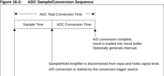
Figure 16-2 shows a basic conversion sequence and the terms that are used. A sampling of the analog input pin voltage is performed by Sample/Hold amplifiers (also called Sample/Hold chan- nels). The 10-bit ADC configuration can use up to four Sample/Hold channels, designated CH0-CH3, whereas the 12-bit ADC configuration can use only one Sample/Hold channel, CH0.
The Sample/Hold channels are connected to the analog input pins via the analog input multiplexer. The analog input multiplexer is controlled by the ADxCHS123 and ADxCHS0 regis- ters. There are two sets of multiplexer control bits in the ADC channel select registers that func- tion identically. These two sets of control bits allow two different analog input multiplexer configurations to be programmed (called MUX A and MUX B). The ADC can optionally switch between the MUX A and MUX B configurations between conversions. The ADC can also option- ally scan through a series of analog inputs.
Sample time is the time that the ADC module’s Sample/Hold Amplifier is connected to the analog input pin. The sample time can be started manually by setting the ADC Sample Enable (SAMP) bit in ADCx Control Register 1 (ADxCON1<1>) or started automatically by the ADC hardware.
The sample time is ended manually by clearing the SAMP control bit in the user software or auto- matically by a conversion trigger source.
Conversion time is the time required for the ADC to convert the voltage held by the Sample/Hold Amplifier. The ADC is disconnected from the analog input pin at the end of the sample time. The ADC requires one A/D clock cycle (T AD ) to convert each bit of the result plus two additional clock cycles. A total of 12 T AD cycles are required to perform the complete conversion in 10-bit mode.
A total of 14 T AD cycles are required to perform the complete conversion in 12-bit mode. When the conversion time is complete, the result is loaded into the ADCxBUF0 register, the Sam- ple/Hold Amplifier can be reconnected to the input pin and a CPU interrupt can be generated.
The sum of the sample time and the A/D conversion time provides the total conversion time.
There is a minimum sample time to ensure that the Sample/Hold Amplifier provides the desired accuracy for the A/D conversion (see 16.15 “A/D Sampling Requirements”). Furthermore, there are multiple input clock options for the ADC. You must select an input clock option that does not violate the minimum T AD specification.
Figure 16-2: ADC Sample/Conversion Sequence
The ADC allows many options for specifying the sample/convert sequence. The sample/convert sequence can be very simple, using only one Sample/Hold amplifier. A more elaborate sam- ple/convert sequence performs multiple conversions using more than one Sample/Hold amplifier.
The 10-bit ADC configuration can use two Sample/Hold amplifiers to perform two conversions in a sample/convert sequence or four Sample/Hold amplifiers with four conversions.
Sample Time ADC Conversion Time ADC Total Conversion Time
Sample/Hold Amplifier is connected to the analog input pin for sampling.
Sample/Hold Amplifier is disconnected from input and holds signal level.
A/D conversion is started by the conversion trigger source.
A/D conversion complete, result is loaded into result buffer.
Optionally generate interrupt.
A D C
16
The number of Sample/Hold amplifiers, or channels per sample, used in the sample/convert sequence is determined by the Channel Select (CHPS<1:0>) control bits in ADCx Control Reg- ister 2 (ADxCON2<9:8>).
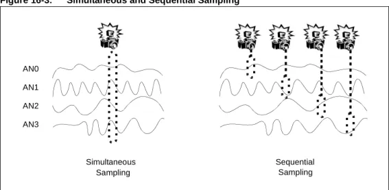
A sample/convert sequence that uses multiple Sample/Hold channels can be simultaneously sampled or sequentially sampled, as controlled by the Simultaneous Sample Select (SIMSAM) bit (ADxCON1<3>). Simultaneously sampling multiple signals ensures that the snapshot of the analog inputs occurs at precisely the same time for all inputs. Sequential sampling takes a snap- shot of each analog input just before conversion starts on that input. The sampling of multiple inputs is not correlated.
Figure 16-3: Simultaneous and Sequential Sampling
The start time for sampling can be controlled in software by setting the ADC Sample Enable (SAMP) control bit (ADxCON1<1>). The start of the sampling time can also be controlled auto- matically by the hardware. When the ADC module operates in the Auto-Sample mode, the Sam- ple/Hold amplifier(s) is reconnected to the analog input pin at the end of the conversion in the sample/convert sequence. The auto-sample function is controlled by the ADC Sample Auto-Start (ASAM) control bit (ADxCON1<2>).
The conversion trigger source ends the sampling time and begins an A/D conversion or a sample/convert sequence. The conversion trigger source is selected by the Sample Clock Source Select (SSRC<2:0>) control bits (ADxCON1<7:5>. The conversion trigger can be taken from a variety of hardware sources, or can be controlled manually in software by clearing the SAMP control bit. One of the conversion trigger sources is an auto-conversion. The time between auto-conversions is set by a counter and the ADC clock. The Auto-Sample mode and auto-con- version trigger can be used together to provide endless automatic conversions without software intervention.
An interrupt can be generated at the end of each sample/convert sequence or after multiple sample/convert sequences, as determined by the value of the Samples Per Interrupt Note: The 12-bit ADC configuration can only perform one conversion in a single sam-
ple/convert sequence. The CHPS bits are irrelevant in this case.
AN0 AN1 AN2 AN3
Simultaneous Sampling
Sequential
Sampling
16.4 ADC MODULE CONFIGURATION
The following steps should be followed for performing an A/D conversion:
1. Select 10-bit or 12-bit mode (ADxCON1<10>)
2. Select voltage reference source to match expected range on analog inputs (ADxCON2<15:13>)
3. Select the analog conversion clock to match desired data rate with processor clock (ADxCON3<7:0>)
4. Select port pins as analog inputs (ADxPCFGH<15:0> and ADxPCFGL<15:0>)
5. Determine how inputs will be allocated to Sample/Hold channels (ADxCHS0<15:0> and ADxCHS123<15:0>)
6. Determine how many Sample/Hold channels will be used (ADxCON2<9:8>, ADx- PCFGH<15:0> and ADxPCFGL<15:0>)
7. Determine how sampling will occur (ADxCON1<3>, ADxCSSH<15:0> and ADxC- SSL<15:0>)
8. Select Manual or Auto Sampling
9. Select conversion trigger and sampling time.
10. Select how conversion results are stored in the buffer (ADxCON1<9:8>) 11. Select interrupt rate or DMA buffer pointer increment rate (ADxCON2<9:5>)
12. Select the number of samples in DMA buffer for each ADC module input (ADxCON4<2:0>)
13. Select the data format
14. Configure ADC interrupt (if required)
• Clear ADxIF bit
• Select interrupt priority (ADxIP<2:0)
• Set ADxIE bit
15. Configure DMA channel (if needed) 16. Turn on ADC module (ADxCON1<15>)
The options for these configuration steps are described in the subsequent sections.
16.5 SELECTING THE VOLTAGE REFERENCE SOURCE
The voltage references for A/D conversions are selected using the VCFG<2:0> control bits (ADxCON2<15:13>). The upper voltage reference (V REFH ) and the lower voltage reference (V REFL ) can be the internal AV DD and AV SS voltage rails or the V REF + and V REF - input pins.
The external voltage reference pins can be shared with the AN0 and AN1 inputs on low pin count devices. The ADC module can still perform conversions on these pins when they are shared with the Vref+ and Vref- input pins.
The voltages applied to the external reference pins must meet certain specifications. Refer to the
“Electrical Specifications” section of the device data sheet for details
A D C
16
16.6 SELECTING THE A/D CONVERSION CLOCK
The ADC module has a maximum rate at which conversions can be completed. An analog module clock, T AD , controls the conversion timing. The A/D conversion requires 12 clock periods (12 T AD ) in the 10-bit mode and 14 clock periods (14 T AD ) in the 12-bit mode. The A/D conversion clock is derived from either the device instruction clock or an internal RC clock source.
The period of the A/D conversion clock is software selected using a 6-bit counter. There are 256 possible options for T AD , specified by the ADC Conversion Clock Select (ADCS<7:0>) bits (ADxCON3<7:0>). Equation 16-1 gives the T AD value as a function of the ADCS control bits and the device instruction cycle clock period, T CY .
Equation 16-1: A/D Conversion Clock Period
For correct A/D conversions, the A/D conversion clock (T AD ) must be selected to ensure a minimum T AD time of 75 nsec.
The ADC module has a dedicated internal RC clock source that can be used to perform conversions. The internal RC clock source should be used when A/D conversions are performed while the device is in Sleep mode. The internal RC oscillator is selected by setting the ADC Con- version Clock Source (ADRC) bit (ADxCON3<15>). When the ADRC bit is set, the ADCS<7:0>
bits have no effect on the A/D operation.
Figure 16-4: A/D Conversion Clock Period Block Diagram T
AD= T
CY(ADCS + 1)
ADCS = T
ADT
CY– 1
0
1
ADC Internal
RC Clock
Clock Multiplier 1, 2, 3, 4, 5,..., 256
ADxCON3<15>
T
CYT
AD8
ADxCON3<7:0>
A/D Conversion
16.7 SELECTING ANALOG INPUTS FOR SAMPLING
All Sample/Hold Amplifiers have analog multiplexers (see Figure 16-1) on both their non-invert- ing and inverting inputs to select which analog input(s) are sampled. Once the sample/convert sequence is specified, the ADxCHS0 and ADxCHS123 registers determine which analog inputs are selected for each sample.
Additionally, the selected inputs can vary on an alternating sample basis or on a repeated sequence of samples.
The same analog input can be connected to two or more Sample/Hold channels to improve con- version rates.
16.7.1 Configuring Analog Port Pins
The ADPCFGH and ADPCFGL registers specify the input condition of device pins used as ana- log inputs. Along with the Data Direction (TRISx) register in the Parallel I/O Port module, these registers control the operation of the ADC pins.
A pin is configured as analog input when the corresponding PCFGn bit (ADPCFGH<n> or ADPCFGL<n>) is clear. The ADPCFGH and ADPCFGL registers are clear at Reset, causing the ADC input pins to be configured for analog input by default at Reset.
When configured for analog input, the associated port I/O digital input buffer is disabled so it does not consume current.
The port pins that are desired as analog inputs must have their corresponding TRIS bit set, spec- ifying port input. If the I/O pin associated with an A/D input is configured as an output, the TRIS bit is cleared and the port’s digital output level (V OH or V OL ) is converted. After a device Reset, all TRIS bits are set.
A pin is configured as digital I/O when the corresponding PCFGn bit is set. In this configuration, the input to the analog multiplexer is connected to AVss.
16.7.2 Channel 0 Input Selection
Channel 0 is the most flexible of the four Sample/Hold channels in terms of selecting analog inputs. It allows you to select any of the up to 16 analog inputs as the input to the positive input of the channel. The Channel 0 Positive Input Select for Sample A (CH0SA<4:0>) bits (ADxCHS0<4:0>) normally select the analog input for the positive input of channel 0.
You can select either V REF - or AN1 as the negative input of the channel. The CH0NA bit (ADxCHS0<7>) normally selects the analog input for the negative input of channel 0.
16.7.2.1 SPECIFYING ALTERNATING CHANNEL 0 INPUT SELECTIONS
The Alternate Input Sample Mode Select (ALTS) bit (ADxCON2<0>) causes the ADC module to alternate between two sets of inputs that are selected during successive samples.
The inputs specified by CH0SA<4:0> (ADxCHS0<4:0>), CH0NA (ADxCHS0<7>), CH123SA (ADxCHS123<0>) and CH123NA<1:0> (ADxCHS123<2:1>) are collectively called the MUX A inputs. The inputs specified by CH0SB<4:0> (ADxCHS0<12:8>), CH0NB (ADxCHS0<15>), CH123SB (ADxCHS0<8>) and CH123NB<1:0> (ADxCHS0<10:9>) are collectively called the MUX B inputs. When the ALTS bit is ‘1’, the ADC module alternates between the MUX A inputs on one group of samples and the MUX B inputs on the subsequent group of samples.
Note: Different devices will have different numbers of analog inputs. Verify the analog input availability against the device data sheet.
Note 1: When the ADC Port register is read, any pin configured as an analog input reads as a ‘0’.
2: Analog levels on any pin that is defined as a digital input (including the AN15:AN0
pins) may cause the input buffer to consume current that is out of the device’s
specification.
A D C
16
For channel 0, if the ALTS bit is ‘0’, only the inputs specified by CH0SA<4:0> and CH0NA are selected for sampling.
If the ALTS bit is ‘1’, on the first sample/convert sequence for channel 0, the inputs specified by CH0SA<4:0> and CH0NA are selected for sampling. On the next sample convert sequence for channel 0, the inputs specified by CH0SB<4:0> and CH0NB are selected for sampling. This pattern repeats for subsequent sample conversion sequences.
Note that if multiple channels (CHPS = 01 or 1x) and simultaneous sampling (SIMSAM = 1) are specified, alternating inputs change every sample because all channels are sampled on every sample time. If multiple channels (CHPS = 01 or 1x) and sequential sampling (SIMSAM = 0) are specified, alternating inputs change only on each sample of a particular channel.
16.7.2.2 SCANNING THROUGH SEVERAL INPUTS WITH CHANNEL 0
Channel 0 can scan through a selected vector of inputs. The CSCNA bit (ADxCON2<10>) enables the CH0 channel inputs to be scanned across a selected number of analog inputs. When CSCNA is set, the CH0SA<4:0> bits are ignored.
The ADCx Input Scan Select Register High (ADxCSSH) and ADCx Input Scan Select Register Low (ADxCSSL) registers specify the inputs to be scanned. Each bit in these registers corresponds to an analog input. Bit 0 corresponds to AN0, bit 1 corresponds to AN1 and so on.
If a particular bit is ‘1’, the corresponding input is part of the scan sequence. The inputs are always scanned from lower to higher numbered inputs, starting at the first selected channel after each interrupt occurs.
The ADxCSSH and ADxCSSL bits only specify the input of the positive input of the channel. The CH0NA bit still selects the input of the negative input of the channel during scanning.
If the ALTS bit is ‘1’, the scanning only applies to the MUX A input selection. The MUX B input selection, as specified by the CH0SB<4:0>, still selects the alternating channel 0 input. When the input selections are programmed in this manner, the channel 0 input alternates between a set of scanning inputs specified by the ADxCSSL register and a fixed input specified by the CH0SB bits.
16.7.3 Channel 1, 2 and 3 Input Selection
Channel 1, 2 and 3 can sample a subset of the analog input pins. Channel 1, 2 and 3 can select one of two groups of three inputs.
The CH123SA bit (ADxCHS123<0>) selects the source for the positive inputs of channel 1, 2 and 3. Clearing CH123SA selects AN0, AN1 and AN2 as the analog source to the positive inputs of channel 1, 2 and 3, respectively. Setting CH123SA selects AN3, AN4 and AN5 as the analog source.
The CH123NA<1:0> bits (ADxCHS<2:1>) select the source for the negative inputs of channel 1, 2 and 3. Programming CH123NA = 0x selects V REF - as the analog source for the negative inputs of channels 1, 2 and 3. Programming CH123NA = 10 selects AN6, AN7 and AN8 as the analog source to the negative inputs of channels 1, 2 and 3 respectively. Programming CH123NA = 11 selects AN9, AN10 and AN11 as the analog source.
Note: If the number of scanned inputs selected is greater than the number of samples
taken per interrupt, the higher numbered inputs will not be sampled.
16.7.3.1 SELECTING MULTIPLE CHANNELS FOR A SINGLE ANALOG INPUT The analog input multiplexer can be configured so that the same input pin is connected to two or more Sample/Hold channels. The ADC converts the value held on one Sample/Hold channel, while the second Sample/Hold channel acquires a new input sample.
16.7.3.2 SPECIFYING ALTERNATING CHANNEL 1, 2 AND 3 INPUT SELECTIONS
As with the channel 0 inputs, the ALTS bit (ADxCON2<0>) causes the ADC module to alternate between two sets of inputs that are selected during successive samples for channel 1,2 and 3.
The MUX A inputs specified by CH123SA and CH123NA<1:0> always select the input when ALTS = 0.
The MUX A inputs alternate with the MUX B inputs specified by CH123SB and CH123NB<1:0>
when ALTS = 1.
16.8 ENABLING THE MODULE
When the ADC Operating Mode (ADON) bit (ADxCON1<15>) is ‘1’, the ADC module is in Active mode and is fully powered and functional.
When ADON is ‘0’, the ADC module is disabled. The digital and analog portions of the circuit are turned off for maximum current savings.
In order to return to the Active mode from the Off mode, the user must wait for the analog stages to stabilize. For the stabilization time, refer to the Electrical Characteristics section of the device data sheet.
16.9 SPECIFYING SAMPLE/CONVERSION CONTROL
The ADC module uses four Sample/Hold amplifiers and one A/D Converter in the 10-bit mode.
The module can perform 1, 2 or 4 input samples and A/D conversions per sample/convert sequence.
16.9.1 Number of Sample/Hold Channels
The CHPS<1:0> control bits (ADxCON2<9:8>) are used to select how many Sample/Hold ampli- fiers are used by the ADC module during sample/conversion sequences. The following three options can be selected:
• CH0 only
• CH0 and CH1
• CH0, CH1, CH2, CH3
The CHPS control bits work in conjunction with the SIMSAM (simultaneous sample) control bit (ADxCON1<3>). The CHPS and SIMSAM bits are not relevant in 12-bit mode as there is only one Sample/Hold amplifier.
16.9.2 Simultaneous Sampling Enable
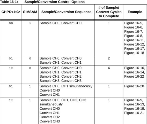
Some applications can require that multiple signals be sampled simultaneously. The SIMSAM control bit (ADxCON1<3>) works in conjunction with the CHPS control bits and controls the sam- ple/convert sequence for multiple channels as shown in Table 16-1. The SIMSAM control bit has no effect on the ADC module operation if CHPS<1:0> = 00. If more than one Sample/Hold ampli- fier is enabled by the CHPS control bits and the SIMSAM bit is ‘0’, the two or four selected chan- nels are sampled and converted sequentially with two or four sampling periods. If the SIMSAM bit is ‘1’, two or four selected channels are sampled simultaneously with one sampling period.
The channels are then converted sequentially. The SIMSAM bit is not relevant in 12-bit mode as there is only one S/H.
Note: The SSRC<2:0>, SIMSAM, ASAM, CHPS<1:0>, SMPI<3:0>, BUFM and ALTS bits,
as well as the ADxCON3, ADxCSSH and ADxCSSL registers, should not be written
to while ADON = 1. This would lead to indeterminate results.
A D C
16
Table 16-1: Sample/Conversion Control Options
16.10 HOW TO START SAMPLING 16.10.1 Manual
Setting the SAMP bit (ADxCON1<1>) causes the ADC to begin sampling. One of several options can be used to end sampling and complete the conversions. Sampling does not resume until the SAMP bit is once again set. For an example, see Figure 16-5.
16.10.2 Automatic
Setting the ASAM bit (ADxCON1<2>) causes the ADC to automatically begin sampling a channel whenever a conversion is not active on that channel. One of several options can be used to end sampling and complete the conversions. If the SIMSAM bit specifies sequential sampling, sampling on a channel resumes after the conversion of that channel completes. If the SIMSAM bit specifies simultaneous sampling, sampling on a channel resumes after the conversion of all channels completes. For an example, see Figure 16-6.
CHPS<1:0> SIMSAM Sample/Conversion Sequence
# of Sample/
Convert Cycles to Complete
Example
00 x Sample CH0, Convert CH0 1 Figure 16-5,
Figure 16-6, Figure 16-7, Figure 16-8, Figure 16-11, Figure 16-12, Figure 16-17, Figure 16-18
01 0 Sample CH0, Convert CH0
Sample CH1, Convert CH1
2
1x 0 Sample CH0, Convert CH0
Sample CH1, Convert CH1 Sample CH2, Convert CH2 Sample CH3, Convert CH3
4 Figure 16-10, Figure 16-14, Figure 16-22 01 1 Sample CH0, CH1 simultaneously
Convert CH0 Convert CH1
1 Figure 16-20
1x 1 Sample CH0, CH1, CH2, CH3
simultaneously Convert CH0 Convert CH1 Convert CH2 Convert CH3
1 Figure 16-9,
Figure 16-13,
Figure 16-19,
Figure 16-21
16.11 HOW TO STOP SAMPLING AND START CONVERSIONS
The conversion trigger source terminates sampling and starts a selected sequence of conversions. The Sample Clock Source Select (SSRC<2:0>) bits (ADxCON1<7:5>) select the source of the conversion trigger.
16.11.1 Manual
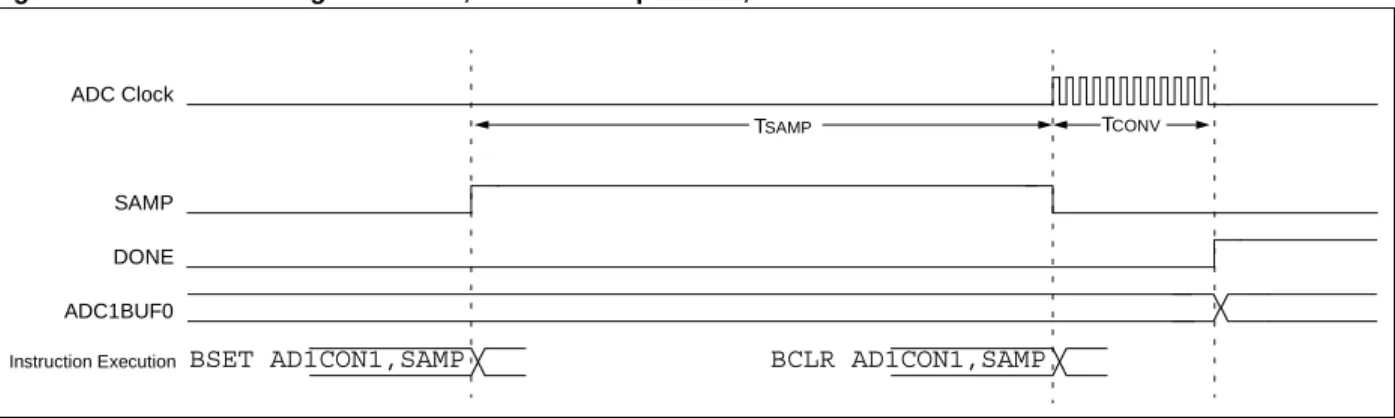
When SSRC<2:0> = 000, the conversion trigger is under software control. Clearing the SAMP bit (ADxCON1<1>) starts the conversion sequence.
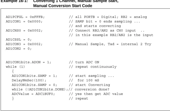
Figure 16-5 is an example where setting the SAMP bit initiates sampling and clearing the SAMP bit terminates sampling and starts conversion. The user software must time the setting and clearing of the SAMP bit to ensure adequate sampling time of the input signal. See Example 16-1 for code example.
Figure 16-5: Converting 1 Channel, Manual Sample Start, Manual Conversion Start
Note: The available conversion trigger sources can vary depending on the device variant.
Please refer to the specific device data sheet for the available conversion trigger sources.
Note: The SSRC<2:0> selection bits should not be changed when the ADC module is enabled. If you change the conversion trigger source, be sure the ADC module is disabled first by clearing the ADON bit (ADxCON1<15>).
ADC Clock
SAMP
ADC1BUF0
T
SAMPT
CONVBCLR AD1CON1,SAMP BSET AD1CON1,SAMP
Instruction Execution
DONE
A D C
16
Example 16-1: Converting 1 Channel, Manual Sample Start, Manual Conversion Start Code
Figure 16-6 is an example where setting the ASAM bit initiates automatic sampling and clearing the SAMP bit terminates sampling and starts conversion. After the conversion completes, the ADC module automatically returns to a sampling state. The SAMP bit is automatically set at the start of the sample interval. The user software must time the clearing of the SAMP bit to ensure adequate sampling time of the input signal, understanding that the time between clearing of the SAMP bit includes the conversion time as well as the sampling time. See Example 16-2 for code example.
Figure 16-6: Converting 1 Channel, Automatic Sample Start, Manual Conversion Start AD1PCFGL = 0xFFFB; // all PORTB = Digital; RB2 = analog AD1CON1 = 0x0000; // SAMP bit = 0 ends sampling ...
// and starts converting
AD1CHS0 = 0x0002; // Connect RB2/AN2 as CH0 input ..
// in this example RB2/AN2 is the input AD1CSSL = 0;
AD1CON3 = 0x0002; // Manual Sample, Tad = internal 2 Tcy AD1CON2 = 0;
AD1CON1bits.ADON = 1; // turn ADC ON
while (1) // repeat continuously
{
AD1CON1bits.SAMP = 1; // start sampling ...
DelayNmSec(100); // for 100 mS AD1CON1bits.SAMP = 0; // start Converting while (!AD1CON1bits.DONE);// conversion done?
ADCValue = ADC1BUF0; // yes then get ADC value
} // repeat
ADC Clock
SAMP
ADC1BUF0
T
SAMPT
CONVBCLR AD1CON1,SAMP Instruction Execution T
CONVBSET AD1CON1,ASAM BCLR AD1CON1,SAMP
T
SAMPT
AD0 T
AD0
DONE
Example 16-2: Converting 1 Channel, Automatic Sample Start, Manual Conversion Start Code
16.11.2 Clocked Conversion Trigger
When SSRC<2:0> = 111, the conversion trigger is under A/D clock control. The Auto Sample Time (SAMC<4:0>) bits (AD1CON3<12:8>) select the number of T AD clock cycles between the start of sam- pling and the start of conversion. This trigger option provides the fastest conversion rates on multiple channels. After the start of sampling, the ADC module counts a number of T AD clocks specified by the SAMC bits.
Equation 16-2: Clocked Conversion Trigger Time
When using only one Sample/Hold channel or simultaneous sampling, SAMC must always be pro- grammed for at least one clock cycle. When using multiple Sample/Hold channels with sequential sampling, programming SAMC for zero clock cycles results in the fastest possible conversion rate.
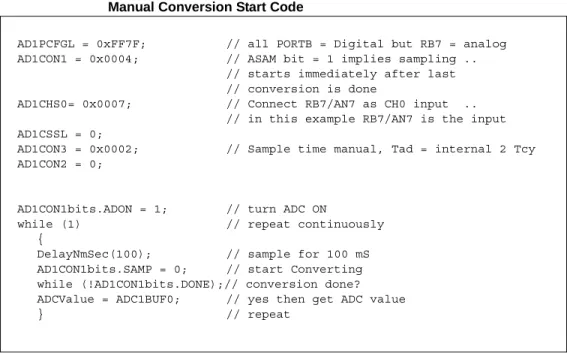
See Example 16-3 for code example.
Figure 16-7: Converting 1 Channel, Manual Sample Start, T
ADBased Conversion Start
AD1PCFGL = 0xFF7F; // all PORTB = Digital but RB7 = analog AD1CON1 = 0x0004; // ASAM bit = 1 implies sampling ..
// starts immediately after last // conversion is done
AD1CHS0= 0x0007; // Connect RB7/AN7 as CH0 input ..
// in this example RB7/AN7 is the input AD1CSSL = 0;
AD1CON3 = 0x0002; // Sample time manual, Tad = internal 2 Tcy AD1CON2 = 0;
AD1CON1bits.ADON = 1; // turn ADC ON
while (1) // repeat continuously
{
DelayNmSec(100); // sample for 100 mS AD1CON1bits.SAMP = 0; // start Converting while (!AD1CON1bits.DONE);// conversion done?
ADCValue = ADC1BUF0; // yes then get ADC value
} // repeat
T SMP = SAMC<4:0>*T AD
ADC Clock
SAMP
ADC1BUF0
T
SAMPT
CONVBSET AD1CON1,SAMP
Instruction Execution DONE
= 16 T
ADA D C
16
Example 16-3: Converting One Channel, Manual Sample Start, T
ADBased Conversion Start Code
16.11.2.1 FREE RUNNING SAMPLE CONVERSION SEQUENCE
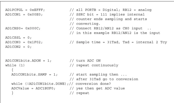
As shown in Figure 16-8, using the Auto-Convert Conversion Trigger mode (SSRC = 111) in combination with the Auto-Sample Start mode (ASAM = 1), allows the ADC module to schedule sample/conversion sequences with no intervention by the user or other device resources. This
“Clocked” mode allows continuous data collection after module initialization.
Figure 16-8: Converting One Channel, Auto-Sample Start, T
ADBased Conversion Start
Note: This A/D configuration must be enabled for the conversion rate of 750 ksps.
AD1PCFGL = 0xEFFF; // all PORTB = Digital; RB12 = analog AD1CON1 = 0x00E0; // SSRC bit = 111 implies internal
// counter ends sampling and starts // converting.
AD1CHS0= 0x000C; // Connect RB12/AN12 as CH0 input ..
// in this example RB12/AN12 is the input AD1CSSL = 0;
AD1CON3 = 0x1F02; // Sample time = 31Tad, Tad = internal 2 Tcy AD1CON2 = 0;
AD1CON1bits.ADON = 1; // turn ADC ON
while (1) // repeat continuously
{
AD1CON1bits.SAMP = 1; // start sampling then ...
// after 31Tad go to conversion while (!AD1CON1bits.DONE);// conversion done?
ADCValue = ADC1BUF0; // yes then get ADC value
} // repeat
ADC Clock
SAMP
Buffer[1]
T
SAMPT
CONVDONE
= 16 T
ADT
SAMPT
CONV= 16 T
ADBuffer[0]
BSET AD1CON1,ASAM
Instruction Execution
16.11.2.2 MULTIPLE CHANNELS WITH SIMULTANEOUS SAMPLING
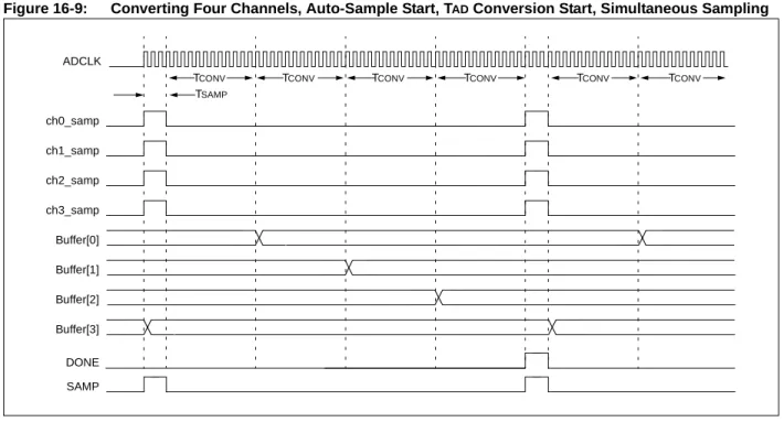
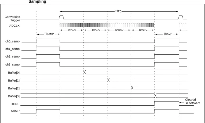
As shown in Figure 16-9 when using simultaneous sampling, the SAMC value specifies the sam- pling time. In the example, SAMC specifies a sample time of 3 T AD . Because automatic sample start is active, sampling starts on all channels after the last conversion ends and continues for three A/D clocks.
Figure 16-9: Converting Four Channels, Auto-Sample Start, T
ADConversion Start, Simultaneous Sampling
16.11.2.3 MULTIPLE CHANNELS WITH SEQUENTIAL SAMPLING
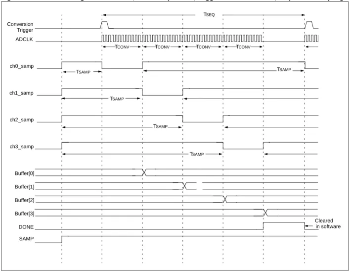
As shown in Figure 16-10 when using sequential sampling, the sample time precedes each conversion time. In the example, 3 T AD clocks are added for sample time for each channel.
Figure 16-10: Converting Four Channels, Auto-Sample Start, T
ADConversion Start, Sequential Sampling
T
CONVT
CONVT
CONVT
CONVADCLK
ch1_samp ch2_samp ch3_samp ch0_samp
Buffer[0]
Buffer[1]
Buffer[2]
Buffer[3]
T
CONVT
CONVDONE SAMP
T
SAMPT
CONVADCLK
ch1_samp ch2_samp ch3_samp ch0_samp
Buffer[0]
Buffer[1]
Buffer[2]
Buffer[3]
T
CONVT
CONVT
CONVT
CONVSAMP
T
SAMPT
SAMPDONE = 0
A D C
16
16.11.2.4 SAMPLE TIME CONSIDERATIONS USING CLOCKED CONVERSION TRIGGER AND AUTOMATIC SAMPLING
Different sample/conversion sequences provide different available sampling times for the Sam- ple/Hold channel to acquire the analog signal. The user must ensure the sampling time exceeds the sampling requirements, as outlined in Section 16.15 “A/D Sampling Requirements”.
Assuming that the ADC module is set for automatic sampling and using a clocked conversion trigger, the sampling interval is determined by the sample interval specified by the SAMC bits.
If the SIMSAM bit specifies simultaneous sampling or only one channel is active, the sampling time is the period specified by the SAMC bit.
Equation 16-3: Available Sampling Time, Simultaneous Sampling
If the SIMSAM bit specifies sequential sampling, the total interval used to convert all channels is the number of channels times the sampling time and conversion time. The sampling time for an individual channel is the total interval minus the conversion time for that channel.
Equation 16-4: Available Sampling Time, Simultaneous Sampling
16.11.3 Event Trigger Conversion Start
It is often desirable to synchronize the end of sampling and the start of conversion with some other time event. The ADC module can use one of three sources as a conversion trigger:
• External INT trigger
• GP Timer Compare trigger
• Motor Control PWM trigger
16.11.3.1 EXTERNAL INT TRIGGER
When SSRC<2:0> = 001, the A/D conversion is triggered by an active transition on the INT0 pin.
The INT0 pin can be programmed for either a rising edge input or a falling edge input.
16.11.3.2 GP TIMER COMPARE TRIGGER
The ADC is configured in this Trigger mode by setting SSRC<2:0> = 010. When a match occurs between the 32-bit timer TMR3/TMR2 and the 32-bit Combined Period register PR3/PR2, a special ADC trigger event signal is generated by Timer3. This feature does not exist for the TMR5/TMR4 timer pair. Refer to Section 11. “Timers” for more details. Check for the most recent documentation on the Microchip website at www.microchip.com.
T
SEQ= Channels per Sample (CH/S) *
((SAMC<4:0> * T
AD) + Conversion Time (T
CONV)) T
SMP= (T
SEQ– T
CONV)
Note 1: CH/S specified by CHPS<1:0> bits.
2: T SEQ is the total time for the sample/convert sequence.
T SMP = SAMC<4:0> * T AD
16.11.3.4 SYNCHRONIZING A/D OPERATIONS TO INTERNAL OR EXTERNAL EVENTS
Modes where an external event trigger pulse ends sampling and starts conversion (SSRC<2:0>
= 001, 10, 011) can be used in combination with auto-sampling (ASAM = 1) to cause the ADC module to synchronize the sample conversion events to the trigger pulse source. For example, in Figure 16-12, where SSRC<2:0> = 010 and ASAM = 1, the ADC module always ends sam- pling and starts conversions synchronously with the timer compare trigger event. The ADC has a sample conversion rate that corresponds to the timer comparison event rate.
Figure 16-11: Converting One Channel, Manual Sample Start, Conversion Trigger Based Conversion Start
Figure 16-12: Converting One Channel, Auto-Sample Start, Conversion Trigger Based Conversion Start
Conversion ADCLK
SAMP ADC1BUF0
T
SAMPT
CONVBSET AD1CON1,SAMP
Instruction Execution
Trigger
ADCLK
SAMP
Buffer[0]
T
SAMPT
CONVBSET AD1CON1,ASAM