1
論 文 の 内 容 の 要 旨
論文題目 Design, Growth, and Characterization of InGaAs/GaAsP Superlattice for High
Efficiency Ge-based Multi-junction Solar Cells
(高効率Geベース多接合太陽電池に向けたInGaAs/GaAsP超格子の設計・評
価および結晶成長に関する研究)
氏 名 藤井 宏昌
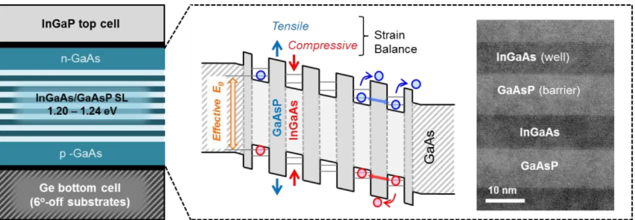
Terrestrial application of III-V based multi-junction solar cells under concentrated sunlight is an innovative solar photovoltaics concept to achieve both high energy conversion efficiency and low power generation cost. InGaP (1.85 eV)/ (In)GaAs (1.42 eV)/ Ge (0.67 eV) lattice-matched system has been widely used as the conventional material combination for Ge-based triple junction solar cells, but the current mismatch due to the wide bandgap of GaAs limits the device performance. Further improvements in cell efficiency are thus expected by extending the absorption edge of the middle cell to approximately 1000 nm, which corresponds to a bandgap below 1.24 eV. InGaAs/GaAsP strain-compensated superlattice (SL) is a promising narrow-bandgap material that can be pseudo-lattice-matched to Ge or GaAs [1]. By alternately growing compressive InGaAs and tensile GaAsP layers with the thicknesses in nanometer scale, a SL with a large number of periods can be epitaxially grown on GaAs.
The purpose of this research is to develop 1.20-1.24 eV band-gap InGaAs/GaAsP (SL) as the middle cell material for Ge-based tandem solar cells, through 1) investigation of the effects of SL on the carrier transport, 2) design of suitable SL layer structure for higher photovoltaic performance, and 3) establishment of metal-organic vapor phase epitaxy (MOVPE) technique to grow high quality SLs on vicinal substrates.
2
In an InGaAs/GaAsP SL solar cell, the SL-region is incorporated in the intrinsic region of the GaAs pin cell as illustrated in the Fig. 1 [2]. Low energy photons can be absorbed and excite generate electron-hole pairs in the InGaAs wells, thus contributing to additional photo-current. A major challenge in such a SL cell is the extraction of the photo-excited carriers through the SL-region, which becomes more difficult by implementing a larger number of wells to absorb sufficient light or applying forward bias to operate the device. In order to clarify the bottleneck problem of SL cell that limits the device performance, this research proposes to use carrier collection efficiency (CCE) to evaluate the carrier transport in solar cells. The CCE is defined as the fraction of carriers photo-generated in the active p-n junction area of a cell, and can be calculated by normalizing the illumination-induced current enhancement to its saturation value at reverse bias (Fig. 2(a)). Combining wavelength- and bias-dependent CCE evaluation, the transport of carriers from each region inside the cell can be examined in detail; the carrier generation distribution can be manipulated by changing the excitation wavelength, and the carrier collection under operational condition can be investigated by applying forward bias. The derivation procedure of the CCE was comprehensively validated by investigating 1) the bias dependence of the absorption in quantum wells, 2) the balance between the amount of absorbed photons and the amount of collectable carriers, 3) the effect of bias sunlight for monochromatic CCE measurement, and 4) the effects of resistance.
The advantage of CCE-based analyses was demonstrated by examining the effectiveness of compensation doping in the i-region. Unintentional p-type background doping due to carbon incorporation during MOVPE causes undesired bending of the band lineup in the i-region, and was found to severely degrade the carrier transport. By compensating the background doping with sulfur to make the electric field uniform in the i-region, transport of the carriers generated anywhere in the device was greatly improved. Furthermore, the challenges in carrier transport for SL cell with a large period number was clarified based on CCE-analyses, in particular for a standard SL design with moderate indium and phosphorus contents (1.2 – 1.7% strain) and relatively thick wells and barriers (> 7 nm); incorporation of a large number of quantum wells significantly thickens the i-region (> 2 m), and thus the carrier transport becomes quite difficult due to the weakened built-in field, especially in the inevitably flattened band even with compensation doping.
In order to overcome the trade-off between light absorption and carrier collection as well as the difficulty in crystal growth of a high-quality SL consisting of strained layers, a stepped tunnel superlattice (STSL) was proposed as a general design principle for quantum well structure in InGaAs/GaAsP SL solar cells. The essential strategies for structural design are: 1) InGaAs wells should be thinner and deeper for a given bandgap for higher absorption coefficient and lower compressive strain accumulation, 2) GaAs interlayers with thicknesses of just a few nanometers are effective for extending the absorption edge to
3
longer wavelengths without additional compressive strain, and for suppressing lattice relaxation during growth, and 3) GaAsP barriers should be thinner than 3 nm to facilitate tunneling transport, and their phosphorus content should be minimized while avoiding detrimental lattice relaxation. In STSL, the carriers in the InGaAs wells are thermionically excited to the upper state and then transported through the thin GaAsP barriers via tunneling as depicted in the Fig. 2(b). The design criteria for individual layers were theoretically and experimentally examined, in particular with systematic investigation of the influences of GaAsP layer design on the carrier transport with various barrier widths (2~6 nm) and phosphorus contents (40~60%). Based on the structural optimization of STSL with an absorption-edge wavelength of 1.23 eV, a P-on-N cell with 100-period In0.30Ga0.70As (3.5 nm)/ GaAs (2.7 nm)/ GaAs0.60P0.40 (3.0 nm)/ GaAs (2.7 nm) STSL significantly improved the middle cell performance compared to the GaAs control cell, indicating a strong potential of the designed SL structure for introduction into Ge-based 3J tandem solar cells.
For actual application for Ge based devices, the designed InGaAs/GaAsP SL is required to be grown on vicinal substrates to prevent formation of anti-phase domains. Growth of SLs on vicinal substrates, however, is likely to cause undulation of the component layers due to formation of step-bunching that easily degrade the crystal with lattice relaxation. Lowering the growth temperature to shorten the diffusion length of the adatom is effective to suppress the layer undulation, but too low temperature may lead to detrimental effects such as low crystal quality and high impurity incorporation. To overcome these problems, low temperature MOVPE using triethylgallium (TEGa) as the gallium source has been developed to grow high-quality SL on vicinal substrates.
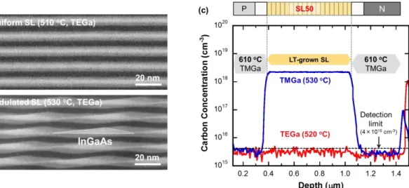
Using TMGa, lattice relaxation due to large step-bunching was significantly prevented by lowering the growth temperature to 550 oC, but severe crystal deterioration apparently occurred below 530 oC because of insufficient atom migration on the crystal surface. The use of TEGa enabled 100-period SLs to be successfully grown at even lower temperature of 510 oC owing to the fast surface reaction as well as the efficient pyrolysis, resulted in a uniform SL with negligible formation of step bunching (Fig. 3(a)). P-type background carbon doping level in the SL grown at 530 oC with TMGa was found to be very high (~1017 cm-3 in bulk GaAs estimated by Hall measurement, ~1018 cm-3 in the SL estimated by SIMS), and compensation doping with sulfur for efficient carrier transport required extremely precise control of the doping level. Substitution of TMGa with TEGa reduced the carbon incorporation owing to its
-elimination reaction that does not produce methyl radicals (Fig. 3(b)), and higher photovoltaic performance than the compensation-doped SL cell grown with TMGa was achieved without performing sulfur doping. Furthermore, growth of compressively-strained STSL with thin GaAsP layers was found to
Fig. 3 TEM images for (a) uniform and (b) undulated SL grown with TEGa, (b) carbon profile in a SL cell grown at low temperature measured by SIMS.
4
be difficult using TMGa because of unstable kinetically-limited growth regime, but was made successful using TEGa.
In order for the optimization of SL growth with TEGa in term of photovoltaic performance, the effects of growth temperature (490-550 oC) and layer undulation on the device properties were further investigated. Larger layer undulation of the SL significantly reduced the light absorbance due to poorer coverage of the InGaAs well region, which was found to be three-dimensionally grown with step bunching at higher temperature as shown in the Fig. 3(b), thus resulting in lower short circuit current (Jsc). The open circuit voltage (Voc), on the other hand, was enhanced by increasing the temperature with reduction of the dark current owing to the higher crystal quality attributed to more complete surface reaction during epitaxy. The layer undulation of the SL was also found to enable more efficient tunnel transport through the thin GaAsP barrier regions, and thus to improve the CCE and the FF. The highest performance was then obtained at a growth temperature of 520-530 oC, at which the SL were quite undulated but the lattice relaxation was avoided.
Toward practical utilization of SL-cells for multi-junction devices, the optimally-designed STSL was implemented into an N-on-P solar cell on a vicinal substrate with the developed growth technique using TEGa. Based on the temperature optimization, N-on-P type 100-period In0.30Ga0.70As (3.4 nm)/GaAs (2.7 nm)/GaAs0.60P0.40 (2.5 nm)/GaAs (2.7 nm) SL cell with bandgap of 1.21 eV was grown on a 6o-off substrate at 520 oC. Due to sufficiently thin GaAsP barriers to facilitate tunnel transport, 60-70% IQE in 850-1000 nm was recorded at 0 V, and the CCE under operational condition remained over 95% over the entire spectrum. Consequently, the SL100-cell achieved 1.11 times higher efficiency with 36% current enhancement as middle cell performance than a GaAs reference cell. Targeted Jmax as a middle cell of 17 mA/cm2 was also achieved as an expected value (17.4 mA/cm2) with anti-reflection coating.
0 5 10 15 0.0 0.2 0.4 0.6 0.8 1.0 GaAs cell SL100 cell Cu rre n t De ns ity (mA/ c m 2 ) Voltage (V) AM1.5 filtered (>665 nm) 0.0 0.2 0.4 0.6 0.8 1.0 400 500 600 700 800 900 1000 1100 GaAs cell SL100 cell Inte rna l Qua nt um E ff ic ie nc y Wavelength (nm) (a) (b)
Fig. 4 (a) I-V characteristics under filtered AM1.5G (>665 nm) and (b) IQE of an N-on-P STSL100 cell and a GaAs reference cell.
References
[1] S. M. Bedair, T. Katsuyama, P. K. Chiang, et al. "GaAsP-GaInAsSb Superlattice: A New Structure f or Electronic Devices," J. Cryst. Growth, 68 (1984) 477-482.
[2] N. J. Ekins-Daukes, J. M. Barnes, K. W. J. Barnham, et al., "Strained and strain-balanced quantum well devices for high-efficiency tandem solar cells," Sol. Energy Mater. Sol. Cells, 68 (2001) 71-87. [3] N. Y. Jin-Phillipp, F. Phillipp, T. Marschner, et al., "Thickness modulation in symmetrically strained
III–V semiconductor superlattices grown by MOVPE," J. Mater. Sci. Mater. Electron. 8 (1997) 289-299.