Chirality selective growth of single-walled carbon
nanotubes using W-Co alloy catalyst
(W-Co 合金触媒を用いたカイラリティ制御
単層カーボンナノチューブ合成)
Hua AN
Doctoral dissertation
Chirality selective growth of single-walled carbon
nanotubes using W-Co alloy catalyst
by
Hua AN
Presented to
GRADUATE SCHOOL OF ENGINEERING, THE UNIVERSITY OF TOKYO
in Partial Fulfillment of the Requirements for the Degree of
Doctoral of Philosophy
in the Field of Mechanical Engineering
i
Ever since their discovery, single-walled carbon nanotubes (SWNTs) have attracted intensive attention because of their unique properties and potential applications. The diversity of SWNT atomic structures provides a broad window for their applications in nanodevices. However, the candidates for individual devices require SWNT assemblies with homogeneous structure and properties. Unfortunately, the as-grown SWNTs are always a mixture of various chiralities, which hinders their applications in nanoelectronics. Since the chirality determines the property of SWNTs, diameter-control and chirality-control are the prerequisite to obtain SWNTs with homogeneous properties. Extensive researches have focused on the direct growth of SWNTs with identical chirality and diameter, however, it is still a critical challenge to grow single-chirality SWNT assemblies. Catalysts play an important role in the chirality definition of SWNTs during the growth. Bimetallic catalysts usually possess different catalytic properties than either of their parental metals and thus they have been widely explored in catalytic reactions for SWNTs growth. In this dissertation, the bimetallic catalysts will be the main focus to selectively control the diameter and chirality of SWNTs.
In order to investigate the mechanism of the growth of SWNTs with transmission electron microscopy (TEM), we have developed an in-plane TEM method where a thin amorphous SiO2 window can work as the substrate to directly grow SWNTs with deposited catalysts. By
using the in-plane TEM method, we have successfully studied the CuCo bimetallic catalyst which can grow small-diameter SWNTs at relatively low temperature. An anchoring effect of Cu has been proposed to prevent the active Co catalyst particles from aggregating to larger ones resulting in the production of small-diameter SWNTs.
Recently, Co7W6 clusters were reported to successfully grow a metallic chirality (12, 6)
SWNT, with over 90% abundance, a zigzag (16, 0) SWNT with near 80% and a semiconducting (14, 4) SWNT with over 97%, by controlling the catalyst structure and
ii
Am. Chem. Soc., 2015, 137, 8688; ACS Nano, 2017, 11: 186]. However, the low yield and
short SWNTs inhibit the large-scale applications of the near single-chirality SWNT assemblies. Here, we report a simple sputtered W-Co catalyst can selectively grow high-quality (12, 6) SWNTs with better uniformity by low pressure chemical vapor deposition at lower temperature than the Nature paper. The abundance of (12, 6) is 50%-70% according to the statistical Raman mapping analysis and optical absorption spectrum of the randomly collected as-grown SWNTs. Parametric study of the W-Co catalyst system demonstrates that the reduction temperature before growth is critical for the selectivity and the intermediate structure, Co6W6C, is identified by the electron diffraction. Moreover, the
catalyst particles are transformed to Co after 5 min-growth. The investigation of catalysts discloses the complicated structure changes before and after CVD growth.
The as-reduced catalyst particles are characterized by EDS mapping to further understand the elemental distribution of nano sized particles and an acid treatment experiment is designed to verify the nonexistence of the trifle amount of pure Co phase. The time-dependent study confirms that the dynamic evolution of catalyst structure is associated with the selectivity towards (12, 6). The Co6W6C is more likely to correlate with the nucleation of (12, 6) cap to
achieve a selective growth. A proposed mechanism reveals the elongated nucleation and growth stage which is strongly dependent on the catalyst structure. The structure evolution of catalyst particles indicates a possible clue for the understanding of selective growth with Co6W6C. The in-plane TEM study with W-Co bimetallic catalyst paves an important way to
iii
Abstract ... i
Chapter 1 Background and introduction to single-walled carbon nanotubes ... 1
1.1 Introduction to single-walled carbon nanotubes ...1
1.2 Structure and properties of SWNTs ...3
1.2.1 Chirality of SWNTs ... 3 1.2.2 Electronic structure of SWNTs ... 6 1.2.3 Phonon structure of SWNTs ... 10 1.3 Synthesis method ...10 1.3.1 Arc discharge ... 10 1.3.2 Laser ablation ... 11
1.3.3 Chemical vapor deposition (CVD) ... 12
1.4 Growth mechanism ...13
1.5 Assembly morphology and potential applications ...15
1.6 Main challenges for the industrial applications ...16
1.7 Motivation, objective and organization of this dissertation ...17
Chapter 2 Experimental methods ... 19
2.1 Preparation methods for catalysts ...19
2.1.1 Dip-coating ... 19
2.1.2 Magnetron sputtering ... 20
2.2 Synthesis of SWNTs ...21
2.3 Characterization of SWNTs ...22
2.3.1 Raman spectroscopy ... 22
2.3.2 Optical absorption spectroscopy ... 26
2.3.3 Scanning electron microscopy (SEM) ... 29
iv
2.3.7 Application of in-plane TEM in the study of synthesis of small-diameter SWNTs with
CuCo ... 34
2.4 Summary ...43
Chapter 3 Selective synthesis of (12, 6) with sputtered W-Co ... 44
3.1 State of art to achieve single chirality of SWNTs ...44
3.1.1 Separation of SWNTs ... 45
3.1.2 Selective synthesis of SWNTs ... 45
3.1.3 Catalysts in the selective growth of SWNTs ... 46
3.1.4 Recent breakthroughs of high selectivity with W-based catalyst ... 47
3.2 Selective growth of (12, 6) with sputtered W-Co ...48
3.2.1 Growth of SWNTs with sputtered W-Co as catalyst ... 48
3.2.2 Characterization of (12, 6) ... 49
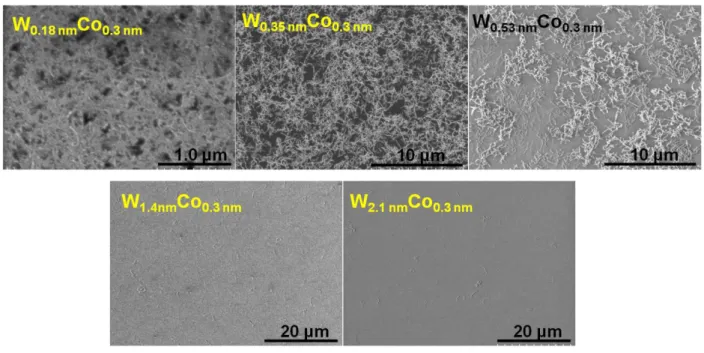
3.3 Parametric study of the selective growth of SWNTs with sputtered W-Co ...56
3.3.1 Influence of the ratio of W to Co ... 57
3.3.2 Effect of reduction temperature ... 59
3.4 Investigation of W-Co catalyst and SWNTs with in-plane TEM ...62
3.4.1 TEM imaging of catalyst morphology ... 62
3.4.2 Electron diffraction pattern of the W-Co catalyst particles ... 64
3.5 Summary ...67
Chapter 4 Structure evolution of W-Co catalyst and the possible mechanism ... 68
4.1 Detailed characterization of as-reduced catalysts ...68
4.1.1 Further confirmation of the as-reduced catalysts by acid treatment ... 69
4.1.2 Elemental distribution of W-Co catalysts ... 70
4.2 Time-dependent growth of SWNTs with sputtered W-Co ...74
4.2.1 Time-dependent growth of SWNTs ... 74
4.2.2 In-plane TEM observation of W-Co catalysts at different growth time ... 75
v
4.2.5 Possible mechanism of the structure evolution of W-Co catalyst during the growth of
SWNTs with ethanol ... 83
4.3 Summary ...84
Chapter 5 Conclusions ... 85
5.1 Summary of the dissertation ...85
5.2 Prospects ...86
Bibliography ... 87
List of abbreviations ... 106
List of publications ... 108
1
Chapter 1 Background and introduction to
single-walled carbon nanotubes
This chapter will give a brief background of single-walled carbon nanotubes which will start with an introduction of carbon, its allotropes and the nanocarbon family. The basic structure and physical properties of single-walled carbon nanotubes will be the main part followed by the widely used synthetic methods and proposed mechanism for SWNTs. Different morphologies of SWNT assemblies reported for various purposes of applications are discussed afterwards. The current main challenges which hinder the industrial applications will be introduced in detail. Finally, the motivations and objectives of this dissertation and organization for the following four chapters will be the closing part.
1.1 Introduction to single-walled carbon nanotubes
Carbon is regarded as one of the most important elements on earth, consisting of the basic skeleton of organic for living things from as huge as whale to as tiny as virus. Carbon is located at group 14, the middle of the main group, unlike the alkali metals or halogens which can lose or get one electron easily to form a perfect stable state as the noble gases. Out of the nucleus, carbon has six electrons of which four belong to the valence electrons. The atomic structure of carbon is shown in Figure 1.1.
The unique atomic structure gives carbon peculiar chemical properties. Six electrons in carbon occupy three different orbitals that is 1s, 2s, 2p. The four electrons in the outer orbitals do not behave equally in the chemical reactions thus carbon can take two different chemical
2
valences +2 and +4 in compounds, for example CO and CO2. Four outer electrons can
combine with four other electrons to form four covalent bonds in the most stable state which also strengthens the compound. This is the typical micro-structure of diamond through sp3 hybridization, constituting one of the hardest materials on the earth. Another important allotrope is graphite. Graphite is a layered carbon material and the micro-structure unit of one layer of graphite is a hexagon with six carbon atoms. The schematic of the one-layer graphite is shown in Figure 1.2. The six carbon atoms are bonded via sp2 hybridization to form a planar structure with π-π bond perpendicular to the hexagonal plane. These hexagons can combine with pentagons and heptagons to form a football shape molecule-fullerene. This hexagon unit can also extend in planar directions to form one-layer graphite-graphene. By rolling up this graphene layer to form a cylinder with two fullerene hemispheric caps at both ends, that is single-walled carbon nanotubes. Multi-walled carbon nanotubes can be formed by rolling up multi layers of graphene sheets. The corresponding microstructures of these nanocarbons are shown in Figure 1.3.
Figure 1.1 Carbon atomic structure.
Figure 1.2 Schematic of the hexagonal structure of the graphene unit. Reproduced from [1] with permission of The Royal Society of Chemistry.
3
Figure 1.3 Various structures in nanocarbon family. Images are from http://www. photon.t.u-tokyo.ac.jp.
1.2 Structure and properties of SWNTs
Single-walled carbon nantubes (SWNTs) are regarded as rolling up a graphene sheet to a cylinder with a diameter of subnanometers to a few nanometers and a length of more than micrometer scale to form one dimensional material with a high aspect ratio and possess excellent structure-dependent mechanical, optical, physical and thermal properties. The structure of SWNTs is determined by the way of rolling-up which in turn defines their properties [2, 3].
1.2.1 Chirality of SWNTs
The definition of chirality of SWNTs comes from the symmetry of the structure when rolling up the graphene sheet. Figure 1.4 shows the unrolled graphene hexagonal lattice structure. a1
and a2 are the unit vectors which can be expressed with the bond length of a graphene
4 a1= ( 2 3 ac-c, 2 3 ac-c), a2= ( 2 3 ac-c, -2 3 ac-c),
According to the relationship in regular hexagon, there is a=| a1|=| a2|= ac-c=2.46 Å which is
the lattice constant of graphene, thus the vectors can also be
a1= ( 2 3 , 2 1 )a, a2=( 2 3 ,-2 1 )a,
The rolling way of graphene sheet to be a SWNT can be determined uniquely by the chiral vector Ch which can be expressed by the unit vectors a1 and a2 as
Ch = na1 + ma2 ≡ (n, m)
And Ch is the radial direction of the rolled-up single-walled carbon nanotube. In this
coordinate, the integer pairs of (n, m) can be used to uniquely define a single-walled carbon nanotube, thus (n, m) is one important index to denote the chirality of SWNTs and normally for convenience, we specify n≥m.
Figure 1.4 Unrolled graphene lattice showing the definition of the chirality of SWNTs. Image is from http://www. photon.t.u-tokyo.ac.jp.
The circumference of the SWNT is | Ch |= ac-c n2 nmm2 , so the diameter of the
5 dt= h C = ) m + nm + (n a 3 c-c 2 2 ∝ n2 nmm2
For the definition of a SWNT, another important vector is the translation vector T in Figure 1.4, which is the shortest repeat distance along the axial direction. T can be expressed as
T= t1a1 + t2a2 ≡ (t1, t2) The relationship of (t1, t2) to (n, m) is t1= R d n 2m , t2 =-R d m 2n
where dR is the greatest common divisor of (2m+n, 2n+m) and can be
dR =
, i n-m is n t a multiple , , i n-m is a multiple .
where d is the greatest common divisor of (n, m).
The area of chiral vector Ch and transition vector T defines the unit cell of the SWNT, and the
number of hexagons, N, in this area is
N= 2 1 h a a T C = R 2 2 d nm) + m + 2(n
As shown in Figure 1.4, the angle between chiral vector Ch and unit vector a1 is defined as
the chiral angle θ, which is given by n an m as
θ= tan-1 ( n m 2 m 3 )
The chiral angle ranges from 0o to 30o (0o ≤ θ ≤ 0o). When θ is 0o, it is a zigzag SWNT, and i θ is 0o
6
important index to denote the chirality of SWNTs as shown in Figure 1.5.
SWNTs can be divided into metallic and semiconducting SWNTs according to their electronic properties, as shown in the chiral map in Figure 1.5.The SWNTs can also be either left handed or right handed, but generally, the handedness of SWNTs does not significantly affect their physical properties and can be experimentally detected only when external fields are applied. Thus we do not discuss the handedness when we talk about the chirality of SWNTs.
Figure 1.5 Chiral map of SWNTs where one pair of (n, m) indice represents one chirality of SWNTs and the black open circles are the semiconducting SWNTs and the red solid circles represent the metallic SWNTs.Image modified from http://www. photon.t.u-tokyo.ac.jp.
1.2.2 Electronic structure of SWNTs
The electronic structure of SWNTs can be understood by imposing a zone-folding effect on the 2D graphite material with tight-binding calculation method since the SWNTs can be formed by rolling up the one layer 2D graphite [2].
Figure 1.6 shows the unit cell of 2D graphene in real space and reciprocal space with the Brillouin zone of 2D graphite in gray hexagon. The unit vector in reciprocal space can be given by
7 b1=( a 3 2 , a 2 ), b2=( a 3 2 , -a 2 )
where a is the lattice constant of graphene in real space and the lattice constant in reciprocal space is 4π/ a. The high symmetry p ints are en te as Г, M, K sh wn in Figure 1.6 at the center, center of edge and the corner respectively. The reciprocal lattice vector K1 in the
circumferential direction and K2 along the axial direction are corresponding with the chiral
vector Ch and the transitional vector T in the real space and define the discrete k values for
the Brillouin zone of a SWNT. The K1 and K2 correlate to Ch and T as
Ch •K1 =2π, T•K1 =0, Ch •K2=0, T•K2 =0.
Thus
NK1 =(-t2b1+t1b2), NK2 = (mb1-nb2).
The first Brillouin zone of a SWNT is a series of cutting lines in the circumferential direction shown in Figure 1.6c. The N wave vect rs μK1 (μ= 0, …, N-1) bring about N discrete k
vect rs r parallel cutting lines an each the μ iscrete values c rresp n s t ne electronic energy band and 6 branches in the phonon dispersion relations. The length of the parallel lines is 2π/T. The spacing between the cutting lines is 2π/Lt with a SWNT length of
Lt which will be continuous wave vectors if the SWNT length extends to infinity due to the
translational symmetry of T.
Figure 1.6 (a) Unit cell of the 2D graphene in real space. (b) Brillouin zone (shaded hexagon area) for 2D graphene in reciprocal space. (c) Brillouin zone for (4, 2) SWNT in reciprocal space. Reprinted from [2], Copyright (2005), with permission from Elsevier.
8
Figure 1.7a sh ws the electr nic ispersi n the irst Brill uin z ne r m the π an π* bands close to the Fermi level of 2D graphite with the tight-binding calculation. K points are the corners where the valence and conduction bands touch together and around there optical transitions can occur. By superimposing the cutting lines from SWNT reciprocal space on this electronic dispersion surface, we can get the electronic band structure of a SWNT given by
Eμ(k)= Eg2D(k 2 2 K K +μK1), (μ=0, … N-1, and - π <k<π)
As shown in Figure 1.7b, if the cutting lines pass across the K points of the Brillouin zone, the certain (n, m) SWNT is metallic with a zero band gap, otherwise, the SWNT is semiconducting with a nonzero band gap between valence and conduction bands. According to the calculation, the condition for metallic SWNTs is that the (n-m) is a multiple of 3. As shown in Figure 1.5, one third of indices are metallic and the other two thirds are semiconducting, which means the as-grown sample will have 67% of semiconducting SWNTs and 33% of metallic SWNTs if all the SWNTs in the chiral table are equivalently grown. In fact, due to the curvature effect, only armchair SWNTs are truly metallic, while other metallic (n-m=3d, d≠0) SWNTs are only gapless at room temperature but will have a small chirality-dependent band gap with deceasing temperatures.
Figure 1.7 Three dimensional band structure of (a) 2D graphene layer (Image from: http://www. photon.t.u-tokyo.ac.jp and http://flex.phys.tohoku.ac.jp) and (b) a SWNT calculated from the nearest neighbor tight bonding model. Reprinted from [2], Copyright (2005), with permission from Elsevier.
9
Of particular importance pertaining to semiconducting SWNTs is that the band gap is independent of chiral angle but relies on the reciprocal nanotube diameter dt with an equation
t c -c d a | t | g E
With this relation, we can conclude that the band gap of semiconducting SWNTs is inversely proportional to their diameter.
Figure 1.8 One dimensional density of states for metallic (12, 6) and semiconducting (6, 5). Images modified from http://www. photon.t.u-tokyo.ac.jp.
Figure 1.9 Kataura plot with the relation of transition energies vs the diameter of SWNTs. Image modified from http://www. photon.t.u-tokyo.ac.jp.
Figure 1.8 shows the density of states of typical metallic and semiconducting SWNTs. A certain chirality of SWNT possesses a specific set of van Hove singularities (vHS) and can exhibit corresponding sets of optical transitions leading to the structural determination of (n,
10
m) by optical experiments. The energy transitions within vHS are labeled as Eii values and
specific to a definite (n, m) SWNT. The relationship of Eii for (n, m) to its diameter is shown
in Figure 1.9 with tight binding calculation which is called Kataura plot. The electronic energy transitions Mii for metallic SWNTs and Sii for semiconducting SWNTs play an
important role in the interpretation of optical spectra for the assignment of (n, m).
Thus the property of SWNTs can be defined by their structure which provides a diversity of applications in electronic devices making SWNTs one of the most promising building blocks in nanoelectronics.
1.2.3 Phonon structure of SWNTs
Similar to the electronic structure, the phonon structure of SWNTs can also be interpreted by the phonon dispersion relations of 2D graphene sheet with a 1D quantum confinement [2]. Thus the phonon density of states for a certain SWNT can be obtained by a zone folding effect which is applicable to most of the phonon modes but needs to be corrected with additional physical concepts for the low frequency region. On the other hand, the Raman signals originate from the corresponding phonon modes with different symmetry which helps us to interpret the Raman spectrum. Phonon structure determines the thermal and mechanical properties of a solid material and also affects the electron transport phenomena. Since the phonon dispersion relations of a SWNT depend on the chirality and diameter of the SWNT, the properties of a SWNT strongly depend on its chirality and diameter.
1.3 Synthesis method
1.3.1 Arc discharge
In the two separate discovery works of single-walled carbon nanotubes, arc discharge is the method to synthesize CNTs with one-atomic-layer wall which is originally used in the production of fullerenes [4, 5]. Typically, in this simple and conventional method, one graphitic composite rod composed of graphite and one single metal or mixed metals is
11
attached to the anode electrode which is coaxial with another carbon rod at a distance of around 1 mm in the chamber [6]. The metal in the composite rod acts as catalyst in the synthetic reaction. Voltage is applied to the electrodes with an electric current across. While operating, the chamber is flowed with inert gas or hydrogen or mixed gas at low pressure. The synthesized SWNTs will deposit on the cathode side. Catalyst is necessary for the growth of SWNTs but in the case of MWNTs, no catalysts are used. The catalyst composites usually include transitional metals Fe, Co, Ni, Pd, Pt etc and their corresponding mixtures with other metals. Accompanied with SWNTs are some other unwanted byproducts such as MWNTs, soot and fullerenes. It will require a post growth purification process before application [7].
Figure 1.10 Schematic of arc discharge method. Reprinted from [6], Copyright (2014), with permission from Elsevier.
1.3.2 Laser ablation
Another high temperature growth method is the laser ablation which was first used for the pr ucti n SWNTs by Smalley’s gr up in 1995 [8]. A high temperature furnace is mounted with a computer controlled laser in the upstream side and a water cooling system at the downstream side. A composite target made of graphite and metal catalyst is placed in the center part of a quartz tube. The chamber is evacuated and then filled with argon gas. SWNTs are produced by laser assisted vaporization and flowed with Ar gas to the collector at the downstream. Diameter of SWNTs can be tuned by varying growth conditions or catalyst compositions to some extent. With this approach, it is still very challenging to scale up the production and purify SWNTs for practical applications because of their highly tangled rope
12
morphology [9].
Figure 1.11 Schematic of the oven laser-vaporization apparatus. Modified from [8], Copyright (1995), with permission from Elsevier.
1.3.3 Chemical vapor deposition (CVD)
Chemical vapor deposition (CVD) is previously used to produce carbon fibers but also show great advantages in the growth of SWNTs [3,10-13]. The decomposition of a hydrocarbon and the deposition of SWNTs can be realized at a much lower temperature than the other two methods. CVD method is versatile and viable for scale-up production of SWNTs for industrial applications and it is easy to control the parameters showing more potential to control the structure and distribution of the as-grown SWNTs. Most importantly, the SWNTs grown from CVD method are of high quality and high purity with low cost. A classic CVD reactor is shown in Figure 1.12. The catalysts are deposited on a flat substrate or support materials in a quartz boat placing under the thermal couple region in the tube chamber. Hydrocarbon gas as the carbon source is flowed and decomposed at the growth temperature. Then SWNTs can be grown on the substrate or support materials with catalysts.
Other setups for CVD system are also available for specific purpose including plasma enhanced CVD and hot filament CVD etc. Other methods which are not widely used in the synthesis of SWNTs will not be introduced in this dissertation. Since the CVD method is more promising in the large-scale production and high-quality and high-purity growth, all the SWNT samples in this dissertation will be grown with CVD method unless otherwise noted.
13
Figure 1.12 Schematic of the CVD furnace. Image modified from [14].
1.4 Growth mechanism
Since their discovery, SWNTs have been produced by various methods using a large variety of metal catalysts and carbon sources with gradually widened growth window [15, 16]. However, the detailed underlying growth mechanism for SWNTs is still under controversy, while many simulations and experimental results show some evidences to disclose a tip of the mysterious story. One of the most popular explanations for the CNT growth is the vapor-liquid-solid (VLS) mechanism [17-19]. However, the hypotheses that the catalyst particles are liquid droplets at growth temperature and the bulk diffusion of carbon are contradictory and misleading [20]. With further modifications and supports, the SWNT growth model by ACCVD method is widely accepted as follows: the ethanol vapor can decompose at the high growth temperature to other carbon species which will be absorbed or adsorbed on the active sites from the catalyst nanoparticles, and the carbon diffusion occur through the corresponding catalyst particles via surface/subsurface diffusion or bulk diffusion. When the particles are saturated, carbon nanotubes can grow from the precipitation of carbon atoms on the catalysts through a top-growth or base-growth model (Figure 1.13).
The decomposition of carbon source molecules can happen at high temperature or due to the promotion of catalyst particles according to the reactivity of carbon sources. Ethanol, acetylene and ethylene can decompose readily at relatively low temperature which is thermodynamically allowed, while the pyrolysis of methane needs higher temperature [20]. Theoretical and experimental results reveal that the products of the carbon source decomposition are small carbon-based molecules or fragments and other byproducts such as
14
dihydrogen [20-22]. However, the reaction intermediate incorporated into the SWNT growth is an open question. Wang et.al claimed a chirality selection induced by single C atom and a growth of SWNTs with the incorporation of C2 dimers based on the abounding density
function calculations [23]. Chains of carbon atoms are also reported as intermediates to proceed the SWNT growth which is the popular “octopus” model in simulations [24]. An isotopically labeled ethanol is proposed by Xiang et.al to demonstrate the unequal contribution of two carbon atoms in ethanol molecules to SWNT growth and the scission of C-C bond and their preferential incorporation to SWNTs [25].
The next debatable issue is the physical state of catalyst particles at the nucleation and growth stage of SWNTs. The melting point of various metal catalysts for the growth of SWNTs is reduced [26] because of the nanosize effect [27] and the influence of carbon [20]. Due to the diversity of catalysts reported for the growth of SWNTs, the physical state of the catalyst particles for some cases is likely to be solid (diamond) and in other cases is probably liquid (Pb, Au) at the standard growth temperatures (600oC-900oC). The in situ TEM observations show the crystal structure during MWNT growth with deformation towards a “pear” shape [28, 29] for the large catalyst particles while the physical state of active catalysts for the growth of SWNTs remains unclear.
The solubility of carbon has been believed to be important for the catalytic ability of metals in the synthesis of SWNTs. An appropriate carbon solubility is required for the carbon diffusion through the catalyst particles [30]. However, the diffusion mode is still under controversy. Generally, the activation barriers for bulk diffusion have been calculated to be significantly higher than that of surface and subsurface diffusions [31]. Insufficient data is available for the dependence of diffusion on the particle size. On the other hand, the chemical state of catalyst during CNT growth is also controversial, especially for the iron catalyst [32]-whether the metal iron or the carbide iron is the real active catalyst for the CNT growth [33-36].
15
semiconducting-pure or chirality-pure properties and much progress has been achieved [37-40]. The selective synthesis of SWNTs always associated with the low yield is mostly contributed to the selective etching effect due to the different reactivity of metallic SWNTs and semiconducting SWNTs [41]. However, the underlying chiral selective mechanism for SWNT nucleation, growth and termination is still unsettled.
Figure 1.13 Schematic of SWNT growth model.
1.5 Assembly morphology and potential applications
From the nanoscale to the microscale, single-walled carbon nanotubes can take on different shapes and morphologies which will influence the properties and further determine their applications [42-46]. In nanoscale, individual SWNTs have been reported to work as optical sensors, transistors and other nanodevices [47-49]. The first sub-10 nm transistor made from one SWNT has been reported to surpassed silicon competitors in 2012 [50]. Individual SWNT can also work as the gate electrode to reduce the size of transistors into 1 nm [51]. In microscale, SWNTs can exhibit different morphologies including vertically-aligned forests (VA-SWNTs) [52], horizontally-aligned arrays [53, 54], randomly transparent conductive films [55] and spun SWNT fibers [56]. VA-SWNT forests can produce a honey-comb microstructure through water vapor treatment to improve the transparency and conductivity of the SWNT film [57]. Transistors that outperform silicon for the first time are created with carbon nanotube arrays [58]. In macroscale, the honey-comb SWNT film can be utilized in Si-based solar cells resulting in a high efficiency [57]. Random SWNT films are promising in
16
the applications of transparent conductive films [59, 60] and flexible electronic devices [61].
Figure 1.14 Assembly morphologies and potential applications of SWNTs at different scales. (a) Reprinted with permission from [50], Copyright (2012) American Chemical Society. (b) From [51], Reprinted with permission from AAAS. (c) Reprinted by permission from Macmillan Publisher Ltd: (Nature Materials) [47], copyright (2004). (d) & (i) Reprinted with permission from [57]. Copyright (2013) American Chemical Society. (f) Reprinted with permission from [54]. Copyright (2013) American Chemical Society. (g) From [46], Reprinted with permission from AAAS. (h) From [62], Reprinted with permission from AAAS. (j) From [59], Reprinted with permission from AAAS. (k) The authors from Ref [61] and the original source of publication from Nature Publishing group are fully acknowledged.
1.6 Main challenges for the industrial applications
SWNTs attract intensive attention due to their structure-dependent mechanical, electrical, thermal and optical properties in widespread applications. SWNTs are reported to be one of the most important promising building blocks in nano devices because of the rich variety of SWNT chiralities [63, 64]. However, the critical obstacles that inhibit the industrial
17
applications of SWNTs are that the conductivity-pure and single-chirality SWNT assemblies with homogeneous property can not be produced. Semiconducting SWNTs are highly desired in electronic devices while the metallic SWNTs can significantly degrade their performance [65]. Single-chirality SWNTs can possess the same properties and display the same response to external stimulations which will dramatically improve the performance of the devices. The expected excellent roles that SWNTs can play in the applications are stranded by the as-grown mixtures of semiconducting and metallic SWNTs with broad chirality distribution [66]. The difficulty for the controlled synthesis of single-chirality SWNTs lies mainly in the lack of proper understanding of growth mechanisms [67]. The experimental investigation to disclose the hidden story in the selective growth of SWNTs requires high resolution in-situ method which is not always possible for researchers. These lead up to the main challenges for the industrial applications of SWNTs-insufficient production and uncompetitive cost of SWNTs, lack of understanding of the growth mechanism, chirality-controlled and diameter-controlled growth of SWNTs.
1.7 Motivation, objective and organization of this
dissertation
As discussed in the last section, the motivation and final objectives in this dissertation is to control the chirality of as-grown SWNTs with bimetallic catalysts and to understand the growth mechanism better with the proposed in-plane TEM method and endeavor to achieve the ultimate goal of single-chirality SWNTs.
Accordingly, the dissertation comprises of three main parts in the following. It will start with the experimental methods used in the synthesis and characterization of SWNTs and catalyst particles. The normal methods are briefly introduced and one novelly developed in-plane TEM is emphasized together with the successful advantages in the study of growth of small-diameter SWNTs using sputtered CuCo catalyst.
18
The most important contributions in this dissertation is the selective growth of (12, 6) SWNTs with sputtered W-Co bimetallic catalyst system. The as-grown SWNTs are characterized with Raman and optical absorption spectroscopy to estimate the content of (12, 6). The catalyst structure is investigated by in-plane TEM method and the crystal structure of catalysts is assigned by electron diffraction.
Further confirmation of the composition of as-reduced catalyst particles is realized and more detailed time-dependent investigation illustrates a complicated structure evolution process with this special bimetallic catalyst which will further guide us in the selective growth of SWNTs.
19
Chapter 2 Experimental methods
The second chapter will mainly focus on the experimental methods for the synthesis and characterization of SWNTs. Sputtering and dip-coating are used for the preparation of catalysts on substrate or supported materials. The as-grown samples are attached with carbon tape to check the morphology of SWNTs with scanning electron microscope (SEM). Renishaw in Via with four different excitation lasers (488 nm, 532 nm, 633 nm, 785 nm) and optical absorption spectroscopy is conducted to characterize the optical response from the SWNT samples. An in-plane TEM method can maintain the original structure of catalyst particles and SWNT morphology on Si/SiO2 microgrid providing an efficacious way to study
the underlying growth mechanism of SWNTs.
2.1 Preparation methods for catalysts
2.1.1 Dip-coating
Dip-coating is a typical and simple method for the preparation of catalysts for SWNT growth which was first introduced in 2003 in our group [68]. This method shows better controllability and uniformity than the drop-casting in the liquid-coating process. The schematic is shown in Figure 2.1. Typically, the cobalt acetate and molybdenum acetate are used as the catalyst precursors which can be tuned according to the purpose. The precursors are dissolved in ethanol solution with a typical concentration of 0.01 wt% and then sonicated for 1 h. During sonication, Si/SiO2 substrate is annealed at 500oC and cooled for 5 min which
20
and yellow for Mo respectively. Once everything is done, the substrate is submerged into the yellow Mo solution for 4 min first, and then withdrawn from the solution with a controlled speed of 6 cm/min. The substrate is annealed at 400oC in a small furnace in air. After cooling down to the room temperature, the substrate is immersed into the pink Co solution with a similar process. Then the prepared substrate is ready for ACCVD growth.
Figure 2.1 Schematic of dip-coating method
2.1.2 Magnetron sputtering
The second important method used for the preparation of catalyst in this dissertation is magnetron sputtering. Magnetron sputtering is established for the deposition of various kinds of coating materials with good controllability and high-quality film and has been widely applied in industrial coating. This method is important for the large-scale coatings especially for the high-melting-point metal and metal oxide [69]. Various parameters including electrode target, power, vacuum pressure and deposition time allow a maximum possibility to control the deposition process. A typical magnetron sputtering is a plasma-assisted deposition process at high vacuum condition. Normally, the chamber is first pumped to 5.0 E-4 to 1.0 E-5 Pa, and inert gas is flowed (Ar gas in our case). With the high electrical field around the target material, Ar plasma ions are created with positive charge and strike the target of the desired coating material. The Ar positive ions have sufficient energy to dislodge the target atoms from the bulk surface, then these atoms eject to the chamber space and some of them can go to the substrate sample and bond on the surface. In the case of CuCo and W-Co bimetallic catalyst systems, silicon substrates are deposited with two different layers of catalyst
21
separately and annealed at 400oC in air right after sputtering. In order to investigate the sequence of different metal materials, sputtering can be done by changing the deposition sequence and co-sputtering method.
Figure 2.2 Schematic of magnetron sputtering method.
2.2 Synthesis of SWNTs
Alcohol catalytic chemical vapor deposition (ACCVD) was first proposed by Maruyama group, and then rapidly developed to grow large-scale carbon nanotubes with high quality and low cost [10]. The detailed setup is shown in Figure 2.3. The aforementioned substrate with catalyst loaded by dip-coating or sputtering is placed in a parallel orientation to the gas flow direction in a quartz tube chamber with the diameter of 25 cm and then pumped to vacuum (typically 25 Pa). Both the sub drain valve and butterfly valve are closed for 5 min to check the leakage of the CVD system. After that, Ar gas is flushed for 5 min to remove water and air in the chamber. After the pretreatment, the chamber is heated to the growth temperature (ranges from 600oC to 900oC) with a mixed Ar/H2 (3%H2) gas to reduce and
anneal the catalyst particles to proper size before the growth of SWNTs. Upon reaching the target temperature, a more 5 min reduction procedure is necessary for further reduction, and then the ethanol gas is introduced to the chamber with a controlled flow rate and pressure. Growth time is determined by detailed purpose which can be easily control. After the growth, ethanol is stopped quickly and the butterfly valve is opened fully and the temperature is reset for cooling with a flushed Ar gas to the room temperature. Finally, the quartz tube is filled
22
with Ar gas and the sample can be taken out for further characterization.
Figure 2.3 Schematic of ACCVD setup. Modified from [70].
2.3 Characterization of SWNTs
In order to analyze the structure and chirality distribution of the as-synthesized SWNTs, various methods are utilized from the optical way such as Raman and absorption spectroscopy to the microscopic way to illustrate the nanoscale single-walled structure by transmission electron microscope (TEM) and the microscale assembly morphology by scanning electron microscope (SEM).
2.3.1 Raman spectroscopy
Raman is a powerful tool for the characterization of materials because of its high sensitivity, easy operation and control, nondestructive measurement, applicability for versatile states of samples (solid, liquid and trace detection) [71].
When the incident light interacts with a material, the light can be absorbed or scattered if the light energy is consistent with the energy gap from the ground state to any exited state. The scattering process can be elastic scattering without energy loss which is the case of Rayleigh scattering or inelastic scattering with the loss of energy which is Raman scattering process.
23
The electrons are excited due to the absorption of energy from the ground state to excited states and will emit photons when return to the lower energy states. This process is Stokes scattering process. On the other hand, if the excited electrons from vibrational states emit photons when relax to the ground state, it is anti-Stokes scattering process. The scattering process can be measured by the intensity of emitted photons with a loss of energy (frequency shift), that is the Raman spectrum [72]. When the excitation energy is close to the energy gap of SWNTs, the Raman scattering intensity is enhanced, and this is due to the resonant effect [73]. Thus Raman scattering of SWNTs is a resonant process selecting specific chiralities whose electronic density of states match with a laser frequency [73].
Figure 2.4 shows a typical Raman spectrum for a SWNT sample with an excitation laser of 488 nm. Three important features from the spectrum can be obtained to interpret the chirality structure and purity of the sample.
One of the most distinct peaks is the G band of SWNTs which is located in high frequency region. The G band at 1590 cm-1 is a typical feature for the hexagonal carbon structure related to the tangential vibrational mode of carbon atoms of SWNTs. Different from the single Lorentzian peak of graphite, G band for SWNTs splits into several peaks due to the confinement of the phonon wave vector along circumferential direction and the symmetry-breaking effects because of the curvature [2]. As shown in Figure 2.4, G band can split into two peaks, G+ band and G- band. G+ band can be assigned to the vibrations of carbon atoms on the graphene cylinder along the axial direction as shown in the vertical arrows in Figure 2.4. On the other hand, G- band originates from the vibrational modes of carbon atoms on the graphene cylinder along the circumferential direction shown as the horizontal arrows in Figure 2.4. The lineshape of G- band is associated with the electronic property of SWNTs [74] and the typical G bands for the metallic and semiconducting SWNTs are shown in Figure 2.4. In the case of metallic SWNTs, a broadened peak of G- band can be observed which is called Breit-Wigner-Fano (BWF) feature related to the charge transfer of SWNTs [75].
24
Figure 2.4 Typical Raman spectra of SWNTs showing different signals with corresponding vibration modes. Image modified from [76]. The authors from Ref [76] and the original source of publication from IOPscience are fully acknowledged.
Of particular importance is that the frequency for G+ band is almost independent on the diameter and chirality, however, for the G- band, the frequency is sensitive to the diameter of SWNTs and the degree of dependency is associated with metallic or semiconducting type of the SWNTs, providing an supplementary method for the judgment of diameter of SWNT sample by Raman spectrum [77].
Another characteristic peak close to G band is D band at around 1320 cm-1. D band is derived from a Raman active disorder mode of symmetry-lowering effect due to the defective hexagonal network from pentagons and heptagons, bending of graphene cylinder, the existence of carbon nanoparticles and amorphous carbon [3]. The intensity of D band is
25
sensitive to the quality of SWNTs which is almost indistinguishable for the highly crystallized and defect-free SWNTs and thus ratio of IG/ID is a good index to evaluate the
quality of as-grown SWNT samples by combining the defective D band and the graphitic G band [78-80].
Figure 2.5 Kataura plot for the relationship of electronic transition energy and SWNT diameter with widened RBM region.
The peaks in the low frequency region (50-500 cm-1) are the radial breathing mode (RBM) correlated to the coherent vibrations of carbon atoms in the radial direction [81]. The RBM feature is unique to single-walled carbon nanotubes and the frequency is inversely proportional to SWNT diameter with a relation of ωRBM=A/dt+B, where A and B are
empirical parameters depending on the surrounding conditions of SWNTs (bundled or not, interaction between SWNT and substrate etc) [82]. With this relation, the diameter of SWNTs can be btaine r m the measurement ωRBM, and the indices of (n, m) can be determined
1001 150 200 250 300 350 400 450 1.2 1.4 1.6 1.8 2 2.2 2.4 2.6 2.8 3 [#94] A. Jorio, PRB 71(2005) 075401 [#50] C. Fantini, PRL 93 (2004) 147406. (12,1) (11,0) (9,1) (7,5) (8,6) (7,6) (11,1) (8,7) (13,0) (9,8) (14,1) (10,0) (6,5) (6,4) (10,1) (7,7) (12,0) (8,8) (9,9) (13,1) (15,0) (10,10) (6,6) (9,0) (9,1) (6,5) (10,0) (11,0) (7,5) (8,6) (7,6) (8,1) (6,4) (16,1) [#960] T. Michel, pssb 243 (2006) 3181 [#95] H. Telg, PRL 93 (2004) 177401. Raman Shift (cm−1) L a se r E n e rg y ( e V ) [#501] P.T. Araujo, PRL 98 (2007) 067401. (8,1) (9,7) 785 nm 633 nm 488 nm 514.5 nm 532 nm 830 nm (14,0) (15,1) (17,0) (16,0) (17,1) (10,8) (10,9) <ES11> <ES22> <EM11> <ES33> (14,1) (13,0) (16,0) (17,1) (19,0) (20,1) (22,0) (18,1) (17,6) (20,0) (10,6) (18,1) (19,1) (21,0) (11,11) (12,12) (13,13) [#96] S.K. Doorn, APA 78 (2004) 1147. <ES44> (8,0) (8,0) (5,4) (5,4) (5,3) (6,1) (5,5) (7,1) (7,0) (5,3) (6,1) 1064 nm
26
by Kataura plot based on the electronic transition energy resonant with the laser wavelength and the nanotube diameter [83]. Figure 2.5 shows the Kataura plot with a widened RBM region from our lab. Owing to the limitation of resonant effect, the RBM peaks from one laser is not a complete detection for the SWNT samples, thus different laser wavelengths are needed for the characterization of the chirality distribution by Raman [84]. It is important to point out that for large-diameter SWNTs, the RBM (less than 50 cm-1) is hardly observable due to the weak intensity [2].
A commercial Renishaw in Via Raman spectroscope will be utilized in this dissertation with four different lasers at the excitation wavelength of 488 nm, 532 nm, 633 nm, 785 nm. The detailed chirality distribution will be discussed in the following chapters for different catalyst systems. A Raman mapping measurement can be readily conducted with this microscope for SWNTs grown on flat substrates. The steps of the mapping arrangement can also be controlled by the commercial software which allows a statistical way of counting the RBM peaks to further analyze the chirality distribution.
2.3.2 Optical absorption spectroscopy
For the synthesis of SWNTs, not only the growth itself is important, but also a quick and reliable characterization which can immediately show the structure and chirality distribution of as-grown SWNTs in the sample is essential for the goal towards selective growth. Even though Raman spectroscopy shows a significant potential in the quick measurement [85], there are also some limitations. Because of the resonant effect, the signals from Raman spectrum in RBM region can only show a limit number of SWNTs existing in the sample [86]. For the RBM peaks excited by one laser, we can not tell the content of each chirality by comparing the peak intensity. The continuous laser is possible for detecting all the existing SWNTs but it seems not applicable for all laboratories. Photoluminescence excitation spectroscopy (PL) can act as a more powerful way to characterize the chirality distribution of dispersed SWNT samples showing the unambiguous identification of chiralities and the distribution with the peak intensity [87]. However, the PL signals from metallic SWNTs are
27
annihilated by electron-electron scattering and phonon-mediated relaxation process [88], thus the PL can only detect semiconducting SWNTs in the sample [89]. Compared to the previous two optical methods, absorption spectroscopy shows powerful and reliable ability to detect the average diameter of the SWNT samples including metallic and semiconducting SWNTs without resonant effect and is applicable to the SWNT films for non-destructive measurement and dispersed SWNT solutions for individual SWNT chirality assignment [90, 91].
Apart from scattering, when the light interacts with a matter, the incident photons can also be absorbed if the photon energy matches with the energy gap promoted from the ground state to the excited states. According to Beer-Lambert law, the absorbance of a sample is proportional to its thickness with an exponential relation. Due to the unique one dimensional feature of SWNTs, the absorption is strongly related to the discrete vHS of DOS. For a certain SWNT sample, the absorption happens when the energy gap of vHS corresponds to the incident photon energy. The electronic transitions can occur with the same order denoted as S11, S22…
for semiconducting SWNTs and M11… r metallic SWNTs. By re erring t Kataura pl t and
the obtained electronic transition energies from absorption spectrum, chirality distribution of the SWNT sample can be identified. Of the same interest is that the intensity of the absorption is determined by the absorbed photon quantity which is dependent on the content of the corresponding chirality, thus the peak intensity of absorption spectrum indicates the enrichment of a certain chirality. Because of the rich diversity of SWNTs, discrete vHS and different electronic transitions, the absorption may overlap with different chiralities [92]. By combining the Raman spectrum with the optical absorption spectrum, the assignment of (n, m) is more reliable and the quantitative analysis becomes possible.
In the case of SWNT film grown from Co, CoMo and CuCo catalysts, the absorption measurement is taken at solid state which is a quite simple shown in Figure 2.6. A transparent bare quartz substrate is used to measure as the baseline, then the SWNT film on the quartz substrate which is transferred from the Si/SiO2 substrate or grown directly on the fused quartz
28
film, the absorbance peaks are broadened and can be roughly used to evaluate the mean diameter in the film sample shown in figure 2.7.
Figure 2.6 Schematic for the absorption microscopy measurement of SWNT film on quartz substrate.
Figure 2.7 Typical absorption spectrum for the SWNT film.
In the case of SWNT sample grown from W-Co catalyst, since the yield is not high enough to measure directly on the quartz substrate, a more common liquid method is used [93]. The randomly collected samples grown directly on the Si/SiO2 substrate are sonicated in the
deuterium oxide (D2O) solution with sodium dodecyl sulfate (SDS) as a surfactant. Then
centrifugation is conducted in order to remove the scraps from Si/SiO2 substrate and the
stripped catalyst particles. After that, the supernatant is collected. Before measurement, the D2O solution with the same SDS concentration is taken as the baseline, and the SWNT
29
solution is measured as illustrated in figure 2.8. In the well dispersed SWNT solution, individual SWNTs encapsulated by the surfactant show sharp absorbance peaks in the spectrum shown in figure 2.9, and the corresponding chirality can be assigned based on Kataura plot.
Figure 2.8 Schematic for the absorption microscopy measurement of SWNT suspension.
Figure 2.9 Typical absorption spectrum for the dispersed SWNTs.
2.3.3 Scanning electron microscopy (SEM)
SWNTs can take on various morphologies, such as SWNTs forest, mat, grassy network, and individual SWNTs randomly distributed on the substrate. In order to effectively characterize the morphology of SWNTs, scanning electron microscopy is widely used. Researchers have successfully grown horizontally aligned SWNT arrays on crystal substrate based on electrical
30
field, substrate and gas flow guided interaction which can be seen through SEM [94-97]. According to the conductivity of SWNTs, we can judge whether a SWNT is metallic or semiconducting with the different contrast on substrate by SEM [98].
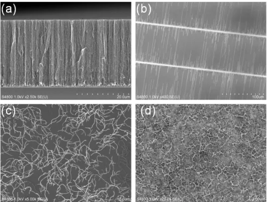
Scanning electron microscopy is a method scanning the surface of a sample with focused fine electron beam and detecting the signals from the sample. The basic signals include for example secondary electrons, back-scattered electrons and so on. Not only the secondary electrons (common mode) but also the back-scattered electrons come from the surface of the sample (within tens of nanometers), thus SEM is a tool to detect the surface topography. The samples for SEM need to be conductive. If not, the samples should be deposited with a thin metal layer on the surface, such as Au. In the case of SWNT samples, it is conductive and can be effectively characterized by SEM. The typical SEM images of SWNTs with different morphologies are shown in Figure 2.10.
Figure 2.10 Typical SEM images of SWNTs with various morphologies. (a) Vertically aligned SWNT forest, (b) Horizontally aligned SWNT arrays, (c) Randomly SWNT network, (d) SWNT thin film on substrate.
31
2.3.4 Transmission electron microscopy (TEM)
Besides SEM, TEM is another powerful means to confirm the existence of CNTs which has played an important role in the breakthrough discovery of multi-walled CNTs and SWNTs [4, 99]. Compared with SEM which detects the secondary electrons or back-scattered electrons for imaging, TEM images the signals after a beam of electrons transmitting and interacting with a thin sample on a layer of photographic film or by a sensor such as a CCD camera. Explicit images of CNTs can be obtained by TEM showing the diameter, wall number, the connection structure with catalyst particles and different morphologies and shapes by high resolution TEM [52, 100]. The existence or nonexistence of catalyst particles can clearly tell the purity of a specimen as shown in figure 2.11.
Figure 2.11 Typical TEM images of SWNTs
2.3.5 Electron diffraction
Because of the feature of wave-particle duality, electron beam can also be regarded as a wave. When electron beam passes through a matter with regular arrangement in atomic level, it can produce a diffraction phenomenon which can be understood by the diffraction of light called Huygens-Fresnel principle [101]. The regular arrangement of atoms can be regarded as an atomic scale lattice plane as shown in figure 2.12. When the incident light interacts with a crystal, the interplanar spacing leads to the interference between the secondary waves and a set of electron diffraction pattern can be generated. The interplanar distance d and the
32
incident angle θ can be relate with wavelength the electr n beam with a Bragg law: nλ = 2 sinθ
I we kn w the electr n wavelength λ, the interplanar istance can be calculate with the obtained electron diffraction pattern and the specific crystal structure can be determined consequently. Electron diffraction represents a viable tool in the field of phase identification. Electron diffraction patterns can exhibit different forms. A pair of spots can be generated with a perfect single crystal sample. However, if the sample is composed of many nano particles in random orientations, the diffraction spots from various planes can form a ring pattern shown in figure 2.13 [102]. The electron diffraction of nanomaterials can be performed in the transmission electron microscope with a selected area region. The resultant selected area electron diffraction pattern can be displayed on a photographic film where a lot of information on the crystal structure can be obtained [103, 104].
Figure 2.12 Schematic of electron diffraction process.
Figure 2.13 Typical electron diffraction patterns for single crystal (Reprinted from [102], Copyright(2016) with permission from Elsevier) and polycrystal samples.
33
2.3.6 In-plane transmission electron microscopy (TEM)
Catalyst plays a critical role in the formation of SWNTs, while obtaining the intrinsic structure and morphology of these nano-sized particles at growth or near-growth conditions remains challenging [105, 106]. Here, we have developed an in-plane TEM approach (figure 2.14) which enables a direct characterization of catalyst particles with atomic resolutions on a amorphous Si/SiO2 micro grid with good uniformity. This microgrid can be stable up to
1000oC which makes direct growth of SWNTs on the microgrid and the in situ TEM observation possible and does not need transfer that means we can get the catalyst structure consistent with wafer substrate and will not lose any information. This in-plane view of catalyst gives comprehensive and statistical information in a large area on the uniform flat substrate from many particles. The collective (rather than localized) information from many particles can be obtained simultaneously by TEM imaging and electron diffraction. With this technique, we will systematically study the behaviors of bimetallic catalysts including CuCo, and W-Co in the growth of SWNTs and propose a possible mechanism accordingly. Sputtering method comes to our eyes due to its uniformity, simplicity and the universality, making it possible to systematically explore all the possible metal catalysts for the growth of SWNTs and their roles in the diameter and chirality control [107].
34
2.3.7 Application of in-plane TEM in the study of synthesis of
small-diameter SWNTs with CuCo
Small-diameter semiconducting SWNTs with large band gap are promising alternatives to improve the performance of wide-bandgap semiconductors [108]. Bimetallic catalysts have shown excellent catalytic properties in the synthesis of small-diameter SWNTs [109, 110]. In our previous study, dip-coated CuCo can successfully grow sub-nanometer vertically aligned SWNT forest at low temperature [111]. The CuCo catalyst deposited by sputtering method can be utilized for the investigation of CuCo catalytic growth of small-diameter SWNTs with in-plane TEM method.
To understand the bimetallic effect of CuCo in the growth of SWNTs better, pure Co catalyst is sputtered with the same parameter as a comparison. With the aid of SEM, we can see that sputtered Co can efficiently grow vertically-aligned SWNT forest with high density at a relatively low temperature of 700oC in figure 2.15. What’s in sharp contrast is that the SWNTs grown from CuCo at 700oC show sparse film randomly laying on the substrate with much lower yield than the forest from sputtered Co. By increasing the growth temperature, the yield which can be displayed by the thickness of the film improves to a thick network mat at CuCo800oC. The nice and clean SWNT bundles show “Y-shape” in the SEM images and the thickness the ilm is less than 1.0 μm. The SWNTs grown at 800o
C with both CuCo and Co exhibit a similar morphology. However, compared to the tendency of increasing yield in CuCo system with the increase of temperature, the Co catalyst at 800oC produces less SWNTs than the vertically aligned forest. This may be related to the density of active catalyst particles during CVD process.
The Raman spectra in figure 2.16 show the diameter distribution of SWNTs grown from two catalyst systems at different temperatures which is labeled as Co700oC, CuCo700oC, Co800oC, CuCo800oC. In the RBM region, the peaks at ~100 cm-1 from Co700oC signify the existence of large-diameter SWNTs [112]. Note that the growth of large-diameter SWNTs in CuCo700oC is almost suppressed by the addition of Cu. The low temperature can grow
35
small-diameter of SWNTs which is consistent with the blue shift of the RBM peaks by comparing the 700oC and 800oC samples in CuCo catalyst system. On the other hand, from the perspective of the catalyst, the introduction of Cu can favor the growth of small-diameter SWNTs at both 700oC and 800oC. Furthermore, the reduction of diameter at 700oC is much more significant than that of 800oC with the introduction of Cu into Co catalyst showing an optimum functional temperature of Cu. It indicates that the introduction of Cu can facilitate the growth of small-diameter SWNTs at relatively low temperature which offers a possible strategy to produce large band gap SWNT samples to promote the applications of SWNTs in nanoelectronics [113-115].
What’s more important is that the IG/ID ratio of the as-grown SWNTs is quite high suggesting
a high quality and high purity of SWNTs in the Raman spectrum shown in figure 2.16. Since the frequency of G- peak in Raman spectrum has been claimed to be another method to estimate the diameter of SWNTs and the G- band frequency reduces with the decrease of SWNT diameter while the G+ band stays constant [77], note that the red shift of the G- band in figure 2.16 is more impressive at low temperature and with CuCo bimetallic catalyst indicating the small diameter of SWNTs.
A more visible comparison of the effect of Cu on Co in the synthesis of small-diameter SWNTs at low temperature is shown in the optical absorption spectrum in figure 2. 17. The significant blue shift of the S11 peaks at low growth temperature (from CuCo700oC to
Co700oC) indicates a great reduction of diameter with the introduction of Cu to Co catalyst while the SWNTs grown from Co and CuCo at 800oC show similar absorbance. This interesting result tells us that Cu is more effective in decreasing the diameter of SWNTs at low temperature than that of high temperature. It suggests that an effective strategy to lower down the optimum growth temperature of SWNTs with better diameter controllability may be to utilize an anchoring metal with low melting point. The effect of the metal with low melting point is more effective at low temperature rather than high temperature based on the interaction of the bimetallic components. The optical absorption spectrum of CuCo 700oC
36
shows dominant peaks assigned to (6, 5) and (7, 6). The SWNT film demonstrates a narrow chirality distribution and the dominant S11 and S22 peaks indicate the enrichment of
semiconducting SWNTs suggesting a high potential in the electronic devices where semiconducting SWNTs are highly desirable.
37
Figure 2.16 Raman spectra of SWNTs grown with sputtered Co and CuCo at 700oC and 800oC.
Figure 2.17 Absorption spectra of SWNTs grown with sputtered Co and CuCo at 700oC and 800oC.
38
In order to investigate the possible mechanism and propose a practical explanation of the growth of small-diameter SWNTs with CuCo at low temperature, the in-plane TEM method is conducted. CuCo bimetallic catalyst and monometallic Co catalyst for control experiment were prepared by magnetron sputtering on the Si/SiO2 microgrid with exactly the same
parameters of wafer substrate. The two microgrids were then undergone a heating process in 300 sccm Ar/H2 (3%H2) and reduced at 700oC for 5min. After the reduction, the furnace was
then cooled down to room temperature and the grids were kept in an Ar/H2 (3%H2)
environment for the whole night before TEM observation to minimize the oxidation of the reduced metallic particles. Figure 2.18a and b show the resultant TEM images of Co and CuCo catalyst. Co particles in a few nanometers are uniformly distributed on the microgrid substrate. Metallic Co and oxidized Co particles due to the exposure to air are displayed with different contrast in which dark parts are metallic Co while the weak contrast ones are CoO because of the different scattering factors [116] and the lattice structure can be recognized in the high-resolution transmission electron microscopy (HRTEM). In the case of CuCo, large particles spread on the microgrid with different contrast in different parts showing the property of polycrystallinity. Among them, small particles intersperse around the larger ones showing two sets of nanoparticles with different sizes. The detailed size distribution of two catalyst systems is summarized and fitted in the histogram in Figure 2.18 b and d. The Co catalyst is fitted by a Gaussian curve showing a narrow size distribution ranging from 2 nm to 5 nm at an average diameter of 3.5 nm. Different from the Co catalyst and consistent with the TEM images, CuCo bimetallic catalyst exhibits a bimodal size distribution fitted by two Gaussian curves at an average size of 1.72 nm and 6.80 nm respectively. The introduction of Cu to Co catalyst system results in narrower-distributed small-size particles and broader-distributed larger-size particles. The role of substantial change of catalyst size on the growth of small-diameter SWNTs needs further investigation.
39
Figure 2.18 TEM imaging of Co and CuCo catalyst and size distribution of the particles. (a) Imaging of sputtered Co particles reduced at 700oC. (b) Imaging of sputtered CuCo particles reduced at 700oC. (c) Size distribution and the fitted corresponding Gaussian curve of sputtered Co particles from (a). (d) Size distribution and the fitted corresponding Gaussian curves of sputtered CuCo particles from (b). Reproduced from [111] with permission from the Royal Society of Chemistry.
To detect the composition of the particles in CuCo catalyst system, elemental mapping of these nanoparticles by energy dispersive X-ray spectroscopy-scanning transmission electron microscopy (EDS-STEM) is shown in figure 2.19. The overlapped elemental distribution of Co and Cu indicates that Co atoms can be either a monometallic Co particle or anchored by Cu atoms in a binary elemental particle. Furthermore, the actual size of the Co aggregates in both binary particles and individual Co clusters is smaller than the size of particles in mono Co metallic catalyst system by the comparison between Figure 2.18a and Figure 2.19a. Note that the Co nanoparticles are not fully encapsulated by Cu atoms but some parts are exposed outside. Moreover, even though Cu can also act as a catalyst in the synthesis of SWNTs [117-119], the low efficiency of Cu catalyst in ACCVD in the previous result (not shown here) and the large diameter of Cu particles suggest that SWNTs in CuCo system may be only
![Figure 1.11 Schematic of the oven laser-vaporization apparatus. Modified from [8], Copyright (1995), with permission from Elsevier.](https://thumb-ap.123doks.com/thumbv2/123deta/8496157.922518/23.892.164.745.156.357/figure-schematic-vaporization-apparatus-modified-copyright-permission-elsevier.webp)
![Figure 2.13 Typical electron diffraction patterns for single crystal (Reprinted from [102], Copyright(2016) with permission from Elsevier) and polycrystal samples](https://thumb-ap.123doks.com/thumbv2/123deta/8496157.922518/43.892.213.684.859.1073/typical-electron-diffraction-reprinted-copyright-permission-elsevier-polycrystal.webp)


![Figure 3.5 Raman spectra of SWNTs with multi data excited at 633 nm. Reproduced from [170]](https://thumb-ap.123doks.com/thumbv2/123deta/8496157.922518/65.892.276.624.99.424/figure-raman-spectra-swnts-multi-data-excited-reproduced.webp)