Japan Advanced Institute of Science and Technology
JAIST Repository
https://dspace.jaist.ac.jp/
Title
Transport properties of field-effect transistor
with Langmuir-Blodgett films of C_<60> dendrimer
and estimation of impurity levels
Author(s)
Kawasaki, Naoko; Nagano, Takayuki; Kubozono,
Yoshihiro; Sako, Yuuki; Morimoto, Yu; Takaguchi,
Yutaka; Fujiwara, Akihiko; Chu, Chih-Chien; Imae,
Toyoko
Citation
Applied Physics Letters, 91(24):
243515-1-243515-3
Issue Date
2007
Type
Journal Article
Text version
publisher
URL
http://hdl.handle.net/10119/4028
Rights
Copyright 2007 American Institute of Physics.
This article may be downloaded for personal use
only. Any other use requires prior permission of
the author and the American Institute of Physics.
The following article appeared in (Naoko
Kawasaki, Takayuki Nagano, Yoshihiro Kubozono,
Yuuki Sako, Yu Morimoto, Yutaka Takaguchi,
Akihiko Fujiwara, Chih-Chien Chu, and Toyoko
Imae, Applied Physics Letters91(24), 243515
(2007)) and may be found at
http://link.aip.org/link/?apl/91/243515.
Transport properties of field-effect transistor with Langmuir-Blodgett films
of C
60dendrimer and estimation of impurity levels
Naoko Kawasaki, Takayuki Nagano, and Yoshihiro Kubozonoa兲
Research Laboratory for Surface Science, Okayama University, Okayama 700-8530, Japan
Yuuki Sako, Yu Morimoto, and Yutaka Takaguchi
Graduate School of Environmental Science, Okayama University, Okayama 700-8530, Japan
Akihiko Fujiwara
Japan Advance Institute of Science and Technology, Ishikawa 923-1292, Japan
Chih-Chien Chu and Toyoko Imae
Faculty of Science and Technology, Keio University, Yokohama 223-8522, Japan
共Received 9 October 2007; accepted 23 November 2007; published online 14 December 2007兲 Field-effect transistor 共FET兲 device has been fabricated with Langmuir-Blodgett films of C60
dendrimer. The device showed n-channel normally off characteristics with the field-effect mobility of 2.7⫻10−3cm2V−1s−1at 300 K, whose value is twice as high as that共1.4⫻10−3cm2V−1s−1兲 for
the FET with spin-coated films of C60 dendrimer. This originates from the formation of ordered
-conduction network of C60moieties. From the temperature dependence of field-effect mobility, a
structural phase transition has been observed at around 300 K. Furthermore, the density of states for impurity levels was estimated in the Langmuir-Blodgett films. © 2007 American Institute of
Physics. 关DOI:10.1063/1.2824818兴
Various types of thin film field-effect transistor 共FET兲 devices were fabricated with spin-coated films of 关6,6兴-phenyl C61-butyric acid methyl ester and C60-fused
N-methylpyrrolidine-meta-C12 phenyl 共C60MC12兲.1,2 The FET device with C60MC12 showed the relatively high value共⬃0.6 cm2V−1s−1兲 because this fullerene related ma-terial could result in the self-assembled films which take 2.32 nm period bilayer structures with interdigitated dodecyl chains.2Recently, we have fabricated the FET devices with the spin-coated films of C60dendrimer关Fig.1共a兲兴 developed
by Takaguchi and co-workers,3,4 and the value was 1.4 ⫻10−3cm2V−1s−1 at 300 K5
. The channel conduction is based on network through the C60 moieties. Further, the
Langmuir-Blodgett 共LB兲 films can be formed with the C60 dendrimer, as shown in Fig.1共b兲,4 and the LB films are ex-pected to form more ordered arrangement of C60 moieties
than in the spin-coated films. In the present study, we have fabricated the FET devices with the LB films of C60
den-drimer and investigated their FET properties.
The structure共top-contact type兲 of the FET device with the LB films of C60dendrimer is shown in Fig.1共c兲. The LB
films composed of five layers of C60dendrimer were used as the active layers of the FET device. The thickness can be estimated to be⬃15 nm. The procedure of the formation of LB films is described elsewhere.4The channel length L and channel width W were 5m and 6 mm, respectively. The thickness of Au source/drain electrodes was 50 nm. The ca-pacitance per area C0was 8.63⫻10−9F cm−2for SiO
2. The
FET properties were measured under high vacuum of 10−6Torr. The atomic force microscope共AFM兲 image of the
LB films is shown in Fig.1共d兲; the AFM image of LB films containing a defect is positively shown so that the LB is clearly recognized to be formed on Si/SiO2 substrate from
the contrast. The Si/SiO2 surface was found to be covered
with LB films of C60dendrimer without defects over several
square micrometers on the basis of the AFM images mea-sured for some Si/SiO2/LB substrates.
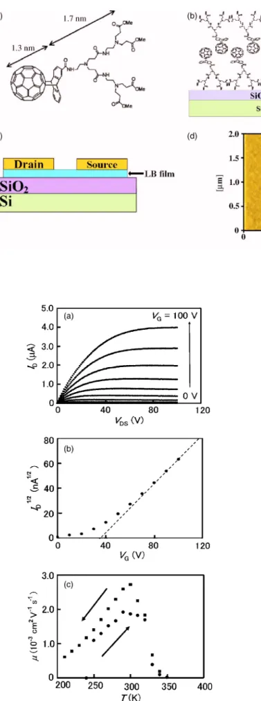
Figure 2共a兲 shows the drain current ID versus
drain-source voltage VDS plots for the FET with the LB films of
C60 dendrimer at 300 K; the annealing was carried out at 60 ° C for 12 h under vacuum of 10−6Torr before the FET
measurement. The plots show typical n-channel normally off output characteristics. The value ofwas determined to be 2.1⫻10−4cm2V−1s−1 at 300 K from the I
D 1/2-V
Gplot关Fig. 2共b兲兴 at saturation regime of VDS= 100 V with general
for-mula for FET analysis;6 the reached the value of 2.7 ⫻10−3cm2V−1s−1 at 300 K by a repetition of annealing, as
shown in Fig. 2共c兲. The value is twice as high as that obtained for the FET with spin-coated films of C60dendrimer 共1.4⫻10−3cm2V−1s−1 at 300 K兲. The higher performance
in the FET with the LB films than in the spin-coated film FET can be attributed to the formation of well-ordered -conduction path. The value of threshold voltage VTH was 36 V 关Fig. 2共b兲兴. No FET properties were observed in the FET device with the L of 30m, suggesting that the ordered region in the LB films is still smaller than 30m, while the FET properties with spin-coated films could be observed at
L = 30m.5In the spin-coated films, the conduction path was easily formed even at the L of 30m because of the thicker films共⬃1m兲 than the LB films 共⬃15 nm兲. The on-off ratio reached 107 in the LB film FET.
The temperature共T兲 dependence ofvalue in the FET device with the LB films is shown in Fig.2共c兲. Thevalue increases with an increase in T up to 300 K, and thevalue decreased rapidly above 300 K; the maximum value was 2.7⫻10−3cm2V−1s−1 at 300 K, as described above. The
drastic decrease is also observed in that reported for the FET device with the spin-coated films.5 As the drastic decrease above 300 K recovers when cooling the T, this transition cannot be ascribed to neither the degradation of the a兲Electronic mail: [email protected]
APPLIED PHYSICS LETTERS 91, 243515共2007兲
0003-6951/2007/91共24兲/243515/3/$23.00 91, 243515-1 © 2007 American Institute of Physics
C60-dendrimer molecule nor the evaporation of the solvents
incorporated into the LB films. Furthermore, the reversible transition of the powder sample of C60dendrimer was found
at around 300 K by the differential scanning calorimetry. Consequently, this transition probably corresponds to the structural order-disorder of C60-dendrimer LB films.
Thevalue for the LB film FET increased by a factor of 2 in comparison with that for the spin-coated film FET. This result is inconsistent with the first expectation that the highly ordered -conduction network in the LB film FET should remarkably increase the value in comparison with that in the spin-coated film FET. From the expectation of the well-ordered C60-moiety network in the LB films, which was
sup-ported by the x-ray reflection,4 we assumed that the charac-teristics of the LB film FET are not still governed by the formation of well-ordered -conduction network between the C60 moieties but by the impurity levels formed into the
LB films. In order to evidence this assumption, we have estimated the density of states N共兲 for the impurity levels which exists in the LB films and compared the N共兲 with that for C60 thin film FET formed by the thermal deposition.
Here, is the energy measured from the lowest unoccupied molecular orbital共LUMO兲 level.
As seen from the schematic energy band diagram in the LB film FET shown in Fig.3共a兲, the LUMO level which is associated with n-channel conduction is lowered by applying the VG 共⬎0兲, and the activation energy Ea, i.e., the energy
difference between the impurity levels matching the Fermi level of electrodes and the LUMO level, should decrease gradually. The Eavalues were determined by a least-squares
fitting with ID⬃exp 共−Ea/kBT兲 to the ID-T plot in the T
region of 260– 310 K at each VGof 40– 100 V 共in 1 V step兲
and at the fixed VDSof 100 V; kBis Boltzmann constant. The Ea-VGplot is shown in Fig. 3共b兲, and the Ea decreases
mo-notonously with an increase in VG, which is consistent with
the behavior expected from the energy band diagram 关Fig.
3共a兲兴. The N共兲 for the impurity levels is given by N共兲 = C0/e关1/共dEa/dVG兲兴, where e is the electronic charge;
7 is
approximately equal to Ea as expected from the energy
dia-gram 关Fig. 3共a兲兴. The N共兲 for the C60-dendrimer LB film
FET is shown as a function of in Fig.3共c兲 together with FIG. 1. 共Color online兲 共a兲 Molecular structure of C60-dendrimer molecule used in this study,共b兲 structure of LB films of C60dendrimer,共c兲 the device structure of the LB film FET, and共d兲 AFM image of LB films used for the FET device. This AFM image contains a defect in which the surface is not covered with the LB films.
FIG. 2.共a兲 Output and 共b兲 transfer characteristics for the LB film FET. In 共b兲, the ID1/2-VGplot at VDS= 100 V is drawn together with the fitting line with general formula for FET analyses共Ref.9兲. 共c兲-T plots for the LB film FET. The symbols쎲 and 䊏 refer to thevalues obtained in increasing and decreasing T, respectively.
243515-2 Kawasaki et al. Appl. Phys. Lett. 91, 243515共2007兲
N共兲- plot for the C60FET; the N共兲 is given by a logarith-mic scale. Since the N共兲 values in low region below 0.15 eV are scattered in the C60FET, the scattered N共兲 val-ues are ruled out in the analyses described in the subsequent paragraph.
The N共兲 was 1019– 1020 cm−3eV−1for both LB film and
C60 FETs. The trapped carriers are assumed to exist within
5 – 10 nm of the interface between active layers and gate di-electric on the basis of the results reported so far,7,8 and actually, the trapping depth of 7.5 nm was used for the N共兲 estimation. As seen from Fig.3共c兲, the N共兲 for the LB film FET in the region of 0.15–0.4 eV is approximately four times as high as that for the C60thin film FET which exhibits
thevalue of 0.14 cm2V−1s−1. This result suggests that the
lower value 共2.7⫻10−3cm2V−1s−1兲 in the LB film FET
than that 共0.14 cm2V−1s−1兲 in the C60 FET can be closely
related to the N共兲 for the impurity levels. The N共兲- plots were well fitted by N共兲=N0exp共−兲, and the N0 and 
were determined to be 8.1⫻1019cm−3eV−1and 6.4 eV−1for
the LB FET, respectively, and 2.0⫻1019cm−3eV−1 and
5 eV−1 for the C
60 FET. Consequently, the N共兲 for the
C60-dendrimer LB film FET showed only an exponential
de-cay with an increase in. The structureless behavior is dif-ferent from the N共兲 for the single crystal pentacene FET, which exhibits a peak ascribable to the impurity levels pro-duced from the bias-stressed defects of pentacene as well as an exponential decay.7 Therefore, the LB film FET is scarcely affected by the bias stress.
Finally, we have calculated the values of subthreshold swing S for the C60-dendrimer LB film and C60 thin film
FETs from the N共兲 of the impurity levels with S=共kBT/e兲
共ln 10兲关1+eN共兲/C0兴,
9
where N共兲 is given in unit
共cm−2eV−1兲. In this estimation, the N共兲 values were used at
the same VG共⬍VTH兲 as those used in the determination of
experimental S values from ID-VG plots, i.e., N共兲=1.91
⫻1012cm−2eV−1 at =0.54 eV and V
G= 25 V for the LB
FET and N共兲=1.61⫻1012cm−2eV−1 at =0.50 eV and VG= 55 V for the C60FET. The S values were estimated to be
2.2 V/decade for the LB FET and 1.8 V/decade for C60FET from the N共兲 and the above equation. These values were 1/5 times the experimental S values, 10.2 V/decade for the LB FET and 7.9 V/decade for the C60FET, determined from ID-VGplots. Nevertheless, the increase in experimental S
val-ues from 7.9 V/decade 共C60 FET兲 to 10.2 V/decade 共LB FET兲 can be completely correlated with the increase in S from 1.8 V/decade共C60FET兲 to 2.2 V/decade 共LB FET兲
es-timated from the N共兲 values, i.e., the ratio of the increase is the same for both S values from the ID-VG and from the N共兲, suggesting that a relative relation of N共兲 between LB
and C60 films is reliable. The deviation of the absolute S
value estimated with N共兲 from that with ID-VGplot may be
ascribed to the factors other than N共兲 such as the increase in off current produced by the measurements under light condi-tion.
The authors are grateful to Mr. Yohei Ohta and Mrs. Michie Sasaki for their kind assistance through this work. This work was partly supported by NEDO and by a Grant-in-Aid共No. 18340104兲 from MEXT, Japan.
1Th. B. Singh, N. Marjanovic, G. J. Matt, N. S. Sariciftci, R. Schwödiauer, and S. Bauer, Appl. Phys. Lett. 85, 5409共2004兲.
2M. Chikamatsu, S. Nagamatsu, Y. Yoshida, K. Saito, K. Yase, and K. Kikuchi, Appl. Phys. Lett. 87, 203504共2005兲.
3Y. Takaguchi, Y. Sako, Y. Yanagimoto, S. Tsuboi, J. Motoyoshiya, H. Aoyama, T. Wakahara, and T. Akasaka, Tetrahedron Lett. 44, 5777 共2003兲.
4C. Hirano, T. Imae, S. Fujima, Y. Yanagimoto, and Y. Takaguchi, Langmuir 21, 272共2005兲.
5H. Kusai, T. Nagano, K. Imai, Y. Kubozono, Y. Sako, Y. Takaguchi, A. Fujiwara, N. Akima, Y. Iwasa, and S. Hino, Appl. Phys. Lett. 88, 173509 共2006兲.
6S. M. Sze, Semiconductor Devices: Physics and Technology共Wiley, New York, 2002兲.
7D. V. Lang, X. Chi, T. Siegrist, A. M. Sergent, and A. P. Ramirez, Phys. Rev. Lett. 93, 086802共2004兲.
8A. R. Völkel, R. A. Street, and D. Knipp, Phys. Rev. B 66, 195336 共2002兲.
9J.-P. Colinge and C. A. Colinge, Physics of Semiconductor Devices 共Klu-wer, Boston, 2002兲.
FIG. 3. 共Color online兲 共a兲 Schematic energy diagram for the LB film FET. Fis the Fermi level for the C60-dendrimer LB films, and at VG= 0 V, the Fermi level of electrodes matches with theF.共b兲 Ea-VGplot for the LB FET.共c兲 N共兲- plots for the LB and C60FET.
243515-3 Kawasaki et al. Appl. Phys. Lett. 91, 243515共2007兲