Japan Advanced Institute of Science and Technology
JAIST Repository
https://dspace.jaist.ac.jp/
Title
ドーピングによりグラフェンナノリボン内化学ポテン
シャルを空間的に制御した量子ドット形成の研究
Author(s)
Wang, Zhongwang
CitationIssue Date
2020‑03‑25
Type
Thesis or Dissertation
Text versionETD
URL
http://hdl.handle.net/10119/16663
RightsDescription
Supervisor:水田 博, 先端科学技術研究科, 博士
氏 名 Wang, Zhongwang 学 位 の 種 類
学 位 記 番 号 学 位 授 与 年 月 日
博士(マテリアルサイエンス)
博材第486号 令和2年3月25日
論 文 題 目 Spatial Chemical Potential Engineering for Quantum Dot Formation in Graphene Nanoribbon via Controllable Doping
論 文 審 査 委 員 主査 水田 博 北陸先端科学技術大学院大学 教授 高村 禅 同 教授 徳光 永輔 同 准教授 赤堀 誠志 同 准教授 西口 克彦 NTT物性科学基礎研究所 特別研究員
論文の内容の要旨
Research Content:
Graphene is of interests to fundamental physics studies as well as to novel applications in electronic devices owing to its many appealing properties such as very high carrier mobility, unique spin quantum Hall effect, high Young’s modulus, etc. It is known that by patterning graphene to a nanoribbon (GNR) with a width of a few tens of nanometer, an effective energy gap can be opened.[1] However, electrons in an etched graphene nanostructure are inevitably subjected to the disorders caused by localized charge states originated from the surrounding environments, e.g., substrate defects, surface adsorptions, organic residues and edge roughness.[2] Interestingly, carriers can tunnel through the isolated localized states enable quantized transport features. [3] By properly control the disorder and their effects, one could either erase the localization features or intentionally build a quantum dot (QD). Suspended graphene, on one hand, is free from substrate disorders, therefore it exhibits almost intrinsic properties. On the other hand, it is difficult to fabricate and fragile. For non-suspended graphene devices, one solution is applying a bias voltage to a local gate. Alternatively, one could introduce chemical doping to a graphene device. By developing a controllable doping method with nanometer scale spatial resolution, we could reconstruct the energy profile of a GNR to a structure similar to a single QD as the illustrated in Fig 1. In this work, we focus on the doping control to realize QD-like single electron transistor (SET) behavior in a solo GNR.
Hydrogen silsesquioxane (HSQ) is a negative tone e-beam resist with a resolution of
~ 20 nm. For GNR, HSQ can be used as etching mask as well as dopant source because HSQ can provide both hydrogen atoms (n-type doping) and oxygen atoms (p-type
doping). Moreover, the spicy and amount of dopants to graphene depends on the e-beam irradiation dose. [5] Thanks to the fine spatial resolution of e-beam lithography technology, we are able to precisely introduce doping to desired position of a GNR by using the dose-controlled e-beam irradiation doping method (see Fig 2). At low temperature (5 K), the expected single QD-like properties, i.e., separate diamond patterns with clear edges, are observed in a doping controlled GNR with a width of 30 nm and a length of 60 nm as shown in Fig 3. The geometry design rule for single QD-like behaviour will be also discussed in the presentation. In addition, a method to fabricate suspended graphene double quantum dot with small deformation will also be introduced for the future prospect.
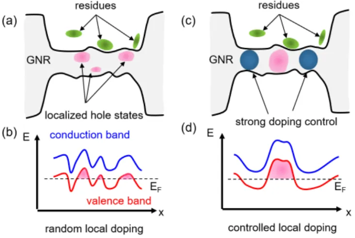
Figure 1. Illustration of the hole localization states and the corresponding energy profile in (a) , (b) non-treated and (c), (d) doping controlled graphene nanoribbons (GNRs). Without any doping treatment, the edge roughness and fabrication residues dominate the energy profile fluctuation (Fig 1 (c)), resulting in random localized hole states in GNR body (Fig 1 (a)). With precise doping control, one can intentionally dope the desired positions of GNR. For instance, on the ends of the GNR (Fig 1 (c)), then the energy profile can be reconstructed as illustrated in Fig 1 (d).
Figure 2. (a) Top profile is the schematic of the designed energy diagram of the controllably doped GNR for constructing a quantum dot. The chemical potential in the center of GNR is ΔED higher than that of the two ends connected to the leads. The middle profile is the geometric design of the HSQ capping layer with varied doses (top). The wide leads (gray) are exposed with a low dose of 900 μC/cm2, whereas the center of the short ribbon (red) is exposed with a high dose of 1800 μC/cm2. Two 8 nm long gaps (blue) inserted between the leads and the GNR are unexposed during lithography. The bottom is the scanning electron microscopic image of the fabricated device scale bar 100 nm. (b) Source-drain conductance (Gsd) verses back gate voltage transfer curves measured in the device with a 30 nm wide and 60 nm long GNR at room temperature and 5 K. Bias Vsd = 1 mV.
At 5 K, a low conductance with oscillation peaks (so called transport gap) is read.
Figure 3. (a) Charge stability diagram measured in the GNR device with the width of 30 nm and length of 60 nm at 5 K. (b) Zoomed-in details of region II in (a) showing the single quantum dot like transport feature. (c) Schematic energy band diagram of the device. Blue and red solid lines indicate the bottom of the conduction band and top of the valence bands, respectively. Fermi levels are
marked corresponding to the four regions, I, II, III, and IV, marked in (a).
References
(1) M. Y. Han, B. Özyilmaz, Y. Zhang and P. Kim, Energy Band-Gap Engineering of Graphene Nanoribbons. Phys. Rev. Lett. 98, 206805, (2007).
(2) D. Bischoff, A. Varlet, P. Simonet, M. Eich, H. C. Overweg, T. Ihn, and K. Ensslin, Localized Charge Carriers in Graphene Nanodevices. Appl. Phys. Rev. 2, 031301, (2015).
(3) C. Stampfer, J. Güttinger, S. Hellmüller, F. Molitor, K. Ensslin and T. Ihn, Energy Gaps in Etched Graphene Nanoribbons. Phys. Rev. Lett. 102, 056403, (2009).
(4) M. Eich, R. Pisoni, H. Overweg, A. Kurzmann, Y. Lee, P. Rickhaus, T. Ihn, K. Ensslin, F.
Herman, M. Sigrist, and K. Watanabe, Spin and Valley States in Gate-Defined Bilayer Graphene Quantum Dots. Phys. Rev. X, 8, 031023, (2018).
(5) K. Brenner and R. Murali, Single Step, Complementary Doping of Graphene. Appl. Phys. Lett.
96, 063104 (2010).
Research Purpose:
Graphene based QD and SET are promise candidates for spin q-bit and ultra-high sensitive charge detector. However, the disorders such as edge roughness and random local doping caused potential profile fluctuation and the consequent multiple QD-like features heavily affect the device properties. It is also believed the disorders are the reason why the promising spin blockade has not been observed so far. To improve the device properties, scientists attend to reduce the impacts of disorders by etching away the SiO
2substrate, using h-BN instead of SiO
2as the substrate, advanced patterning technology, changing the QD design from a disc island to a solo GNR, etc. However, the disorders can not be completely removed by the current technology.
Instead of removing the disorders, we come up with a different concept of doping control. Because in principle, the key to construct QD is a double barrier box to confine the electrons. If we could precisely control over the local doping, we could construct the QD-like potential profile. Therefore, it is not necessary to remove the disorders.
Following this concept, we preformed our experimental studies and investigations. The
key experimental observation is shown in Fig 3. Not only the single-QD like diamond
patterns in Region II, but also the overlapped diamond patterns without clear edges
(signature of multiple QDs, typical transport characteristic in those GNRs without
doping control) in Region IV, indicating the existence of potential fluctuation. Although, we see the single QD-like features in Region II is not affected by the disorders from the experimental results.
Our work on doping controlled GNR provides a new strategy to realize QD. In the future, a local top gate will be attached on the GNR center to tune the potential in the QD region. Also, the single QD GNR will be extended to double, triple QDs with several tuning top gates for the integration experiments.
Key words: graphene nanoribbon, disorder, doping control, single quantum dot, HSQ
論文審査の結果の要旨
グラフェンは特異な電子構造・電界効果特性を持つことから注目され、ナノエレクトロ ニクス応用に向け、盛んに研究されている。特にグラフェン量子ドット中の電子スピンは、
量子コンピュータの基礎となるスピン量子ビットの有力な候補であるため、グラフェン量 子ドットデバイスの研究も活発に行われている。しかし、グラフェンは二次元物質である ため、その単電子・単正孔輸送特性は、グラフェンの周辺環境や微細加工によって生じた チャネルエッジのラフネスに非常に敏感である。特に、残留不純物によるドーピング効果 やエッジラフネスはキャリアの局在化を引き起こし、意図しなかった疑似的量子ドットの 形成を引き起こす。そのため、グラフェンナノ構造内に寸法と帯電エネルギーを制御した
「単一電子島」を形成することは極めて困難であり、これがグラフェン量子ドットデバイ スの開発を妨げてきた。
本研究では、高解像度電子線レジストの一つであるHSQ(Hydrogen Silsesquixane)の Si-HとSi-O結合エネルギーの差に注目し、熱および電子線によって水素と酸素を選択的に グラフェンに局所ドーピングして、グラフェンナノリボン内に閉じ込め静電ポテンシャル 井戸を形成する新たな手法を提案した。これにより、「単一電子島がよく定義された」グラ フェン単キャリアトランジスタ(GSCT)を実現することに成功した。具体的には、HSQのア ニール温度と電子線照射量によるドーピング効果を詳細に分析し、グラフェンナノリボン の電荷中性点変化を制御した。幅と長さを30 nm~110 nmの範囲で変化させた多くのグラ フェンナノリボンを作製し、その電極付近とチャネル中央部分で電子線照射量を局所的に 変化させることで、トンネルバリアと静電ポテンシャル深さを精密に制御したグラフェン 単キャリアデバイスを作製した。そのキャリア輸送特性を温度5K~室温で評価することで、
ナノリボン幅と長さのパラメータ空間上で、トランスポートギャップ特性とクーロン振動 特性のポートフォリオを作成し、理想的な単一ドット・クーロン振動特性が得られる寸法 領域を見出すことに初めて成功した。また、得られた輸送特性を単電子トンネリング理論 と一次元ホッピング伝導モデルで解析し、単一量子ドットの主要物理量であるトランスポ
ートギャップ、トンネル障壁高さ、電子島ポテンシャル深さを定量的に同定するとともに、
実験的に得られたナノリボン幅と長さの設計指針に対する理論的裏付けを見出した。
以上、本論文は、これまで実験的に極めて困難であった「単一電子島」特性を有するグ ラフェン単キャリアトランジスタを作製するユニークなプロセス手法を考案し、得られた 理想的クーロン振動特性の決定因子を初めて明らかにした独創性の高い研究であり、学術 上・応用上両方の観点から極めて価値の高いものである。よって博士(マテリアルサイエ ンス)の学位論文として十分価値あるものと認めた。