The effect of co-doping of nitrogen and
electric field on the magnetism of (Zn,Fe)Te
著者(英)
INDRAJIT SAHA
year
2020
その他のタイトル
(Zn,Fe)Teの磁性に対する窒素ドープおよび電界の
効果
学位授与大学
筑波大学 (University of Tsukuba)
学位授与年度
2019
報告番号
12102甲第9375号
URL
http://doi.org/10.15068/00160447
1
The effect of co-doping of nitrogen and electric field on
the magnetism of (Zn,Fe)Te
INDRAJIT SAHA
2
The effect of co-doping of nitrogen and electric field on
the magnetism of (Zn,Fe)Te
INDRAJIT SAHA
Doctoral Program in Nano-Science and Nano-Technology
Submitted to the Graduate School of
Pure and Applied Sciences
in Partial Fulfillment of the Requirements
for the Degree of Doctor of Philosophy in
Engineering
at the
3
Dedicated to my Parents and Family
with Love and Gratitude
4
Table of Contents
Summary of Thesis ... 7 Chapter 1: Introduction 1.1. Research Background ... 10 1.1.1. Spintronics ... 101.1.2. Diluted Magnetic Semiconductors (DMSs) ... 10
1.1.3. Externally charge co-doped DMSs ... 15
1.1.4. Study of externally applied electric field on DMSs ... 17
1.1.5. Purpose of the present study ... 18
Chapter 2: Basic physical properties and previous research 2.1. The physical properties of II-VI semiconductor compound: ZnTe ... 22
2.1.1. Energy band structure ... 22
2.1.2. Crystal structure of ZnTe ... 23
2.1.3. Previous research on nitrogen (N) acceptor doped ZnTe ... 23
2.2. The physical properties of Zn1-x FexTe DMS ... 28
2.2.1. Theoretical study for the electronic structure of Fe2+ in Zn 1-x FexTe ... 28
2.2.2. Theoretical study for the stability of ferromagnetic state and chemical trend in Zn1-x FexTe ... 30
2.2.3. Experimental report on Fe doped II-VI DMSs ... 32
2.2.4. Experimental report on Zn1-x FexTe bulk crystal ... 33
2.2.5. Previous research on Zn1-x FexTe thin films grown by molecular beam epitaxy (MBE) ... 34
2.3. Theoretical study for co-doping of donor/acceptor impurities in DMSs ... 45
2.4. Research on (Zn,Cr)Te DMS ... 47
2.4.1. Experimental studies on nitrogen (N) acceptor co-doped (Zn,Cr)Te ... 51
2.4.2. Experimental studies on iodine (I) donor co-doped (Zn,Cr)Te ... 57
5
2.6. Experimental studies on electrical field controlled magnetic properties of (In,Mn)As ... 65
2.7. Experimental studies on electrical field controlled magnetic properties of (Ti,Co)O2 ... 67
Chapter 3: Experimental Methods 3.1. Samples preparation by molecular beam epitaxy (MBE) ... 70
3.1.1. Molecular beam epitaxy (MBE) equipment ... 70
3.1.2. Sample preparation ... 73
3.1.3. Reflection high-energy electron diffraction (RHEED) method ... 75
3.1.4. Radiofrequency (rf) plasma source ... 77
3.2. Samples characterization: Compositional analysis of elemental species ... 78
3.2.1. Electron probe micro-analyzer (EPMA) measurement ... 78
3.2.2. Secondary ion mass spectroscopy (SIMS) measurement ... 81
3.3. Structural characterization of samples... 82
3.3.1. X-ray diffraction (XRD) measurement ... 82
3.3.2. X-ray absorption fine structure (XAFS) spectroscopy ... 85
3.3.3. Transmission electron microscope (TEM) observation ... 91
3.4. Magnetization measurement of samples... 93
3.4.1. Superconducting quantum interference device (SQUID) magnetometer ... 93
3.5. Transport properties of samples ... 95
3.5.1. Physical property measurement system (PPMS): Hall measurement ... 95
3.6. Electric field control study ... 99
3.6.1. Formation of electric double layer transistor structure (EDLT) by using liquid electrolyte ... 99
3.6.2. Evaluation of magnetization of samples by SQUID... 100
3.6.3. Electric field control study by using Al2O3 as solid insulating layer ... 102
3.6.4. Atomic layer deposition process of Al2O3 ... 103
3.6.5. ALD device used in this study ... 104
Chapter 4: Experimental results and discussions – I
4.1. Structural and magnetic properties of Zn1-x FexTe: N thin films (Te-rich growth condition) ... 1064.1.1. Sample preparation ... 106
4.1.2. Evaluation of the sample surface by reflection high energy electron diffraction (RHEED) ... 107
4.1.3. Structural analysis of Zn1-x FexTe: N thin films: X-ray diffraction analysis (XRD) ... 107
6
4.1.5. Structural analysis of Zn1-x FexTe: N thin films: Transmission electron microscope (TEM) ... 113
4.1.6. Magnetization measurements of Zn1-x FexTe: N thin films: SQUID ... 115
4.1.7. Transport measurements of Zn1-x FexTe: N thin films: PPMS ... 118
4.1.8. Summary ... 120
4.2. Structural and magnetic properties of Zn1-x FexTe: N thin films (Zn-rich growth condition) ... 120
4.2.1. Sample preparation ... 123
4.2.2. Evaluation of the sample surface by reflection high energy electron diffraction (RHEED) ... 124
4.2.3. Structural analysis of Zn1-x FexTe: N thin films: X-ray diffraction analysis (XRD) ... 125
4.2.4. Structural analysis of Zn1-x FexTe: N thin films: X-ray absorption fine structure (XAFS) ... 126
4.2.5. Magnetization measurements of Zn1-x FexTe: N thin films: SQUID ... 133
4.2.6. Transport measurements of Zn1-x FexTe: N thin films: PPMS ... 139
4.2.7. Summary ... 141
Chapter 5: Experimental results and discussions – II
5.1. Structural and magnetic properties of modulation doped Zn1-x FexTe thin films... 1425.1.1. Sample preparation ... 142
5.1.2. Evaluation of the sample surface by reflection high energy electron diffraction (RHEED) ... 143
5.1.3. Structural analysis of Zn1-x FexTe thin films: X-ray diffraction analysis (XRD) ... 143
5.1.4. Magnetization measurements of Zn1-x FexTe thin films: SQUID ... 145
5.2. Magnetic modulation by applying electric field study ... 146
5.2.1. Sample preparation ... 146
5.2.2. Magnetization measurements of Zn1-x FexTe thin films: SQUID ... 148
5.3. Magnetic modulation of the device structure of Zn1-x FexTe thin films by electric field ... 149
5.3.1. Magnetic modulation by applying electric field using ion polymer as gate insulator ... 149
5.3.2. Possible reason of increase in magnetization during processing ... 151
5.3.3. Summary ... 151
5.3.4. Preparation of Al2O3 layer by ALD method and evaluation of insulating properties ... 151
5.3.5. Magnetic modulation by applying electric field using Al2O3 solid insulating layer ... 152
5.3.3. Future tasks ... 154
Chapter 6: Conclusion ... 155
References
... 157Acknowledgement
... 162Appendix
... 1637
Abstract
The noteworthy mentioning point about most Diluted Magnetic Semiconductors (DMSs) is that the charge state of the magnetic ions and hence, the corresponding interaction energy between them depends on the position of the Fermi level with respect to the band edges of the host semiconductor compound. This property opens an unprecedented opportunity to modify the magnetic properties of DMSs in which the magnetic impurity levels resides within the bandgap of the host semiconductors, by engineering the Fermi level position using co-doping, electric fields or light.
The binding energy of nitrogen acceptor in ZnTe is about 50 meV and can be doped easily, a maximum doping concentration of the order of 1020 cm-3 can be achievable. On the other hand, the Fe 2+ / 3+ donor level is located at
150 meV above the top of the valence band of ZnTe. In addition, the pure dilute phase of zinc-blende structure is obtained for Zn1-xFexTe thin films with Fe composition, x ≤ 0.02 and the isoelectronic Fe2+ state on the
substitutional site of II-VI compounds is found to produce only field-induced magnetic moments, typical van-Vleck type paramagnetic behavior. As the substitutional Fe forms the deep donor Fe2+/3+ levels within the bandgap
of the host ZnTe, the trap of carriers introduced by additional charge doping or application of external gate voltage is expected to deviate the Fe charge state from Fe2+, resulting in a possible modification of magnetic properties. In
this study, we have co-doped nitrogen (N) acceptor impurity and applied external electric field in Zn1-xFexTe thin
films with x ≤ 0.02 to change the valence state of Fe and hence to observe the possible modification of its magnetic properties. The summary of the experimental works is represented under the following headlines:
Structural and magnetic properties of N-doped Zn
1-xFe
xTe thin films with x ≤ 0.02
N-doped Zn1-xFexTe thin films were grown by molecular beam epitaxy (MBE) in the ultra-high vacuum
condition of 10-10 Torr. We have used elemental solid sources of Zn, Te and Fe and nitrogen plasma source with
N2 gas excited by rf-plasma. We have grown Zn1-xFexTe: N thin films under different growth conditions by keeping
Fe composition fixed and varying the N concentrations by changing only the size of holes in the shutter of the plasma source. However, the other N concentration controlling parameters such as, the operating power of the rf-plasma source, the distance between the rf-plasma source and the substrate and the N2 flow rate have been remained
same for a series of samples.
(i) Te-rich growth condition (Te to Zn flux ratio,
𝑻𝒆𝒁𝒏
~ 2.40):
We have investigated the effect of co-doping of nitrogen (N) acceptor impurity on the structural and magnetic properties of Zn1-xFexTe. We grew Zn1-xFexTe: N thin films by MBE with a fixed Fe composition, x = 1.5% and
varied N concentrations in the range of [N] = 8 × 10¹⁷ – 4 × 1019 cm-3. Structural analyses by using x-ray absorption
fine structure (XAFS) reveals that N-doped films with intermediate N concentrations [N] = 8 × 10¹⁷- 7 × 1018 cm -3 are mainly composed of pure diluted phase with substitutional Fe atoms in the valence state deviated from Fe2+
as determined from the shifting of the Fe-K pre-edge peak position towards higher energy in the XANES spectra, while Fe is predominantly incorporated in forming an Fe-N compound at the highest N concentration ,[N] = 4 × 1019 cm-3. According to the previous research on Fe-K pre-edge peak by several research groups, the pre-edge
peak energy position of the XANES spectra is very sensitive to Fe redox states and shifts towards higher energy with increasing oxidation state. The separation between the average pre-edge positions for Fe2+ and Fe3+ states is
1.4 ± 0.1 eV. These results are in agreement with the transmission electron microscopy (TEM) observation where the crystal structure of N-doped film with intermediate N concentration, [N] = 7 × 1018 cm-3 are found to compose
of zinc blende structure; while in the N-doped film with highest N concentration, [N] = 4 × 1019 cm-3, translational
Moire fringes are observed to form at the surface region and consequently, some additional diffraction spots are detected in the corresponding fast Fourier transform (FFT) pattern. Accordingly, the magnetization measurement
8
using SQUID confirms a drastic change of magnetic properties; a linear dependence of magnetization on magnetic field (M-H), typical of van-Vleck paramagnetism in the film without N-doping changes into ferromagnetic behaviors with hysteretic M-H curves at the intermediate N concentrations and comes back to a linear M-H dependence at the highest N concentration. The ferromagnetism in the intermediate [N] range may reflect a deviation of the valence state of the substitutional Fe from Fe2+, while the linear M-H at the highest [N] would be
attributed to precipitates of an Fe-N compound.
(ii) Zn-rich growth condition (Te to Zn flux ratio, 𝑻𝒆
𝒁𝒏 ~ 0.70):
We have also investigated the structural and magnetic properties of nitrogen (N) acceptor impurity co-doped Zn1-xFexTe thin films grown under Zn-rich condition with Fe composition fixed at x = 1.4% and N concentrations
varied in the range of [N] = 1.8 × 10¹⁸ – 5.1 × 1019 cm-3. Structural analysis by X-ray diffraction (XRD) detects
some additional extrinsic diffraction peaks alongside with the intrinsic diffraction peaks from GaAs substrate and ZnTe buffer layer in the N-doped film with the highest N concentration, [N] = 5.1 × 1019 cm-3 only, which may
possibly originate from Fe-N compounds,. This finding is, in agreement with the result of XAFS analysis which shows the shifting of Fe atoms from the substitutional position for N-doped films with higher N concentrations, [N] = 1.8 × 10¹⁹ – 5.1 × 1019 cm-3 ; Whereas, N-doped films with lower N concentrations [N] = 1.8 × 10¹⁸ – 4.3 ×
1018 cm-3 are composed of pure diluted phase with substitutional Fe atoms in the valence state deviated from Fe2+
as determined from the shifting of the Fe-K pre-edge peak position towards higher energy in the XANES spectra. However, the pre-edge peak position is found to be higher as compared to those of Te-rich samples even for the same N concentration. This indicates that the change of valence state from Fe2+ to Fe3+ due to N-doping is more
significant in Zn-rich samples. Consequently, more pronounced change of magnetic properties are observed in the magnetization measurement using SQUID; typical of van-Vleck paramagnetism in the film without N-doping changes into room temperature ferromagnetic behaviors with hysteretic M-H curves for all N-doped films in the N concentrations range of [N] = 1.8 × 10¹⁸ – 5.1 × 1019 cm-3. However, the weak room temperature ferromagnetic
behavior observed in the N-doped films with lower N concentrations, [N] = 1.8 × 10¹⁸ – 4.3 × 1019 cm-3 may reflect
the deviation of valence state of substitutional Fe from Fe2+ to Fe2+/3+ mixed states. On the other hand, the robust
room temperature ferromagnetic behavior observed in the N-doped films with higher N concentrations, [N] = 1.8 × 10¹⁹ - 5.1 × 1019 cm-3 would be attributed to precipitates of Fe-N compounds in which Fe is in Fe2+/3+ or in other
valence state.
The major difference in modification of magnetic properties due to N-doping among Te-rich and Zn-rich growth conditions is observed for N-doped films with N concentration of the order of [N] ≈ 1018 cm-3. In the
Te-rich case, the van-Vleck type paramagnetic behavior of the undoped film changes into low temperature ferromagnetic behavior in the N-doped film with [N] ≈ 1018 cm-3, while in the Zn-rich case, it changes into room
temperature ferromagnetic behavior even for the same N-doping concentration. This difference in magnetic modification can be explained by the observed difference in pre-edge peak position of the N-doped films with same N-doping concentration for these two different growth conditions. The higher energy position of the Fe-K pre-edge peak in the Zn-rich case indicates that the larger deviation of valence state of substitutional Fe from Fe2+
to Fe3+due to N-doping. This large deviation of valence state of substitutional Fe can produce robust finite magnetic
moment even at zero external magnetic field and modify the exchange interaction between magnetic moments. Thus, we get room temperature ferromagnetic behavior in the N-doped films with [N] ≈ 1018 cm-3 grown under
Zn-rich condition.
Structural and magnetic properties of modulation-doped Zn1-xFexTe thin films with x ≤ 0.02
We have studied the structural and magnetic properties of Zn1-xFexTe thin films with Fe composition x = 1.3%
grown on N-doped ZnTe buffer layer with a particular intension to investigate whether the impact of interfacial holes can inducing any exchange interactions and hence alter the magnetic properties of Zn1-xFexTe thin films. The
9
N concentrations of the p-ZnTe layer are of the order of 1019 cm-3. Structural analysis by XRD confirms the absence
of extrinsic precipitate compounds. Diffraction peaks from the ZnTe buffer and GaAs substrate have only been identified. However, the ZnTe peaks for the (400) and (600) diffractions are found to be separated due to N acceptor doping. In the magnetization measurements by SQUID, we have observed different magnetic properties other than the van-Vleck paramagnetic behavior as observed for Zn1-xFexTe thin films grown on the undoped ZnTe
buffer layer. The magnetization result has shown (ordinary) paramagnetic behavior with S-like M-H curve for Zn
1-xFexTe thin films grown on the p-ZnTe buffer layer. This difference of magnetic behavior might reflect the impact
of interfacial holes on the magnetic properties of Zn1-xFexTe.
Effect of external electric field on the magnetism of Zn1-xFexTe thin films with x ≤ 0.02
We have also constructed field effect transistor and electric double layer transistor device structure by using Al2O3 film and liquid electrolyte respectively as gate insulator and Pt foil as gate electrode to module the magnetic
properties of Zn1-xFexTe thin films of Fe composition, x = 1.3%.We have measured the magnetization of the Zn
1-xFexTe thin films after the application of external gate voltages across the device structures by using SQUID. In
both cases, we have followed the measurement sequence 0V → +V → -V → 0V(Re). The magnetic modulation by external gate voltages across the field control device using ionic liquid is found irreversible. The saturation magnetization decreased from the initial value at VG = 0V after the application of positive gate voltage, VG =
+1.5V, but after that there is apparently no change of magnetization with the change of external gate voltages of the order of VG = -2.5V and finally VG = 0V (Re). So, it is believed that the modulation of magnetization may not
originate from the change of intrinsic magnetic properties of Zn1-xFexTe. One possibility of this irreversible
behavior may be the anion and cation in the ionic liquid used for the insulating layer did not move when the gate voltage is switched from positive to negative and even, if returned to 0V. Another reason may be any chemical reaction between ionic liquid and Zn1-xFexTe layer or interface. Unfortunately, we have also not seen any
modulation of magnetic properties after the application of external gate voltages, VG = ± 10V and ± 20V across
the channel layer of Zn1-xFexTe using the existing field control device consisting of solid Al2O3 insulating layer.
The thin Zn1-xFexTe layer with the thick diamagnetic GaAs substrate may make it difficult to measure the electrical
manipulation of magnetization of the Zn1-xFexTe layer. The magnetization dependent Hall effect may be helpful
to extract the small change in the electrical field controlled magnetic properties of the Zn1-xFexTe layer directly.
The ability to externally control the properties of magnetic materials would be highly desirable from fundamental and technological viewpoints, particularly in view of recent developments in magneto electronics and spintronics. In this study, we have modulated the magnetic properties of dilute phase of zinc-blende structured Zn1-xFexTe thin films by co-doping with nitrogen acceptor impurity, from van-Vleck type paramagnetic without
N-doping to room temperature ferromagnetic with N-doping. We have also performed several trials to modulate the magnetic properties of (Zn,Fe)Te thin films by applying gate voltages, but yet not succeed to find the magnetic modulation in a reversible way.
10
Chapter 1: Introduction
1.1 Research background
1.1.1 Spintronics
In this rapidly growing world, the developments in the fields of electronics and information technologies
depends greatly on the efficient synchronization of the physical properties exhibited by charge and spin of electrons. The newly branch of physics “Spintronics” which deals with both the charge and spin of electrons has blessed the modern technology with new functionalities that even not believed before. For example, the invention of switching the magnetic phase of a ferromagnetic semiconductor reversibly using electric fields which is never observed in the case of a ferromagnet or a semiconductor separately. This is one of the examples of Spintronics devices in the semiconductor fields which is steadily growing now. But there are more mature examples available in the field of magnetic metal multilayers such as, reading heads of high-density hard disks (HDD), magnetic random-access memories (MRAM), etc. The operational principles of these devices can be explained on the basis of giant magnetoresistance (GMR, dependent scattering) and tunnel magnetoresistance (TMR, spin-dependent tunneling). The major advantages of these Spintronics devices are the capability of simultaneous mass storage and processing of information efficiently by exploiting “flipping” spin of electrons instead of shutting electrons around as in modern electronics devices. Thus, we can get the combined attributes of non-volatility, high density, high-speed operation and unlimited read and write endurance, low-power consumption in information processing and storage by using Spintronics devices.1.1.2 Diluted Magnetic Semiconductors (DMSs)
Diluted Magnetic Semiconductors (DMSs) are semiconductor compounds in which a substantial portion of semiconductor atoms are substituted by transition metal or rare earth elements (lanthanides) that produce localized magnetic moments in the semiconductor matrix. Usually, magnetic moments originate from the unfilled 3d or 4f shells of transition metals or rare earths (lanthanides) respectively. For example, transition metal elements like Cr, Mn, Fe, Ni, Co etc. which have net spin can be used in III-V, II-VI, II-IV based semiconductor compounds like GaAs, GaN, ZnO and ZnTe etc. to exhibit the dual characteristics of both semiconductor and magnetic materials. The sp-d interactions between the s, p band carries of host semiconductor and localized d states of the transition metals is responsible for the outstanding properties of this new functional materials. In particular, the mixing between the d electrons of the cation substituted transition metals and p orbitals of the host anions around the transition metals are crucial for this type of interaction. The interaction can be ferromagnetic or antiferromagnetic depending on the impact of the cation-substituted transition metal ions on the number of spin-up and/or spin-down states in the valence band of the host semiconductor.
At the beginning of the DMS study, purified Mn was used to fabricate Mn-doped II-VI bulk alloys by various modifications of the Bridgman method. It was observed that II-VI DMSs show less defect concentrations and can be doped easily with shallow impurities. In addition, it was become possible to explore several novel spin related phenomena by the available magneto-optical and magneto transport techniques. However, several difficulties such as the disorder spin orientations in the absence of applied magnetic field even at very low temperatures due to the random distributions of magnetic ions has been observed. So, the interactions between the magnetic ions was predominantly antiferromagnetic in nature. However, due to the developments of the crystal growth methods far from thermal equilibrium such as, molecular beam epitaxy (MBE), laser ablation, it has now become possible to dope magnetic ions beyond the previously thermal-equilibrium solubility limits. In addition, the electrical activity of the shallow impurities can be enhanced by using the MBE growth process. Accordingly, the efforts of making
11
the II-VI wide band-gap semiconductors based optical devices such as, light emitting diodes (LEDs) and diode lasers emitting in the blue-green region were not possible due to the self-compensation effect during doping. This means that they can be doped by either donor (n-type) or acceptor (p-type) impurity. For example, ZnSe can be doped by shallow donor (n-type) impurity only. Due to the invention of the non-equilibrium MBE technique and the availability of radio-frequency plasma, it has now become possible to dope ZnSe with acceptor (p-type) impurity [1, 2]. In the case of III-V semiconductor compounds based DMSs such as, (Ga,Mn)As in which Mn2+
ions provide both magnetic moments and carriers, the use of low-temperature MBE provides thin films with Mn composition up to 7% and the hole concentration over 1020 cm-3 [3]. The discovery of carrier-induced
ferromagnetism in (Ga,Mn)As and p-type doped (Zn,Mn)Te thin films has allowed to explore the physics and possible applications of previously unavailable combinations of quantum structures and ferromagnetism in semiconductors [4, 5]. Efforts are directed intensively to develop new room temperature ferromagnetic DMSs and describe their properties theoretically.
It has been long appreciated that the physics of particular DMSs can be explained by the position of the levels derived from the open d or f shells with respect to the band-edges as well as by the degree of mixing between the local and band levels [6]. The Vonsovskii model for II-VI compound semiconductors has been represented in Fig. 1.1 (a) to explain the position of 3d localized levels of different transition metals [7]. Transition-metal impurity can provide electrons if the corresponding donor levels lie above the bottom of the conduction band and holes if the acceptor levels reside below the top of the valence band. In such cases, carrier-mediated interaction between magnetic ions have been observed. For example, carrier-induced ferromagnetism is studied in details on (Ga,Mn)As due to the peculiar position of Mn d levels relative to the valence band of GaAs as shown in Fig. 1.1(b). The Mn atoms provide both the spins and holes that tailor the ferromagnetic coupling between the localized spins. Similar mechanism has also been noticed in the case of (Zn,Mn)Te co-doped with nitrogen acceptor impurity. The Mn2+/3+ donor levels locate in the valence band of ZnTe and the isoelectronic Mn2+ will not provide any carriers
in the valence band of the host semiconductor matrix. On the framework of carrier-mediated interaction, the free carriers play an important role for ferromagnetic ordering. So, extrinsic nitrogen acceptor co-doping is required to generate carrier-induced Mn2+ spin-spin interactions in (Zn,Mn)Te. However, it is observed that in most of the
studied DMSs, the impurity band reside in the band gap region of the host semiconductor. In such DMSs, the doping of transition metals will provide only localize magnetic moment, but no additional carrier in the host semiconductor matrix. For example, in the case of (Zn,Cr)Te, the substitutional Cr on the Zn-site forms the deep donor Cr2+/3+ and acceptor Cr1+/2+ levels reside within the bandgap of the host ZnTe semiconductor compounds.
The superexchange or the double exchange has been regarded as the origin of the ferromagnetic interaction in (Zn,Cr)Te [8, 9].
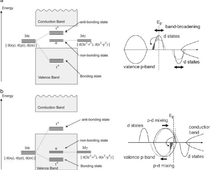
It is now generally believed that the Zener’s p-d exchange and double exchange interactions are the two important mechanism to describe ferromagnetic interactions in semiconductors [10]. According to the theory of ferromagnetic semiconductors, most of the DMSs such as II-VI and III-N semiconductor compound based DMSs belong to the impurity band system, where the Zener’s double exchange is the dominate ferromagnetic exchange mechanism. On the other hand, the Zener’s p-d exchange mechanism can apply only for limited DMSs such as, (Ga,Mn)As, (Ga,Mn)Sb with very shallow impurity levels in the band gap and deep 3d states in the valence band [11]. The schematic electronic structure of a transition metal (TM) impurity at the tetrahedral substitutional site in zinc blende structure for the above two ferromagnetic exchange mechanism is shown in Fig. 1.2 (a) Zener’s double exchange case (b) Zener’s p-d exchange case.
In general, the fivefold degenerate d-states of TM impurity are split into threefold degenerate dε states (xy, yz, zx) and twofold degenerate dγ states (x2-y2, 3z2-r2).The wavefunction of the dε states hybridize strongly with the p-state of anion which make the host valence band, resulting in the bonding states, tb in the valence band and the
counterpart, antibonding states, ta in the band gap as shown in Fig, 1.2 (a). On the other hand, the hybridization of
12
finite concentrations, due to the anti-bonding nature of the ta states, rather broader impurity band (that is,
delocalized) is formed in the band gap. While the impurity band formed by e states are relatively narrow (that is, localized) reflecting their non-bonding character. In the right-side panel of Fig. 1.2 (a), the spin polarized density
Figure 1.1: (a) Approximate positions of levels derived from d shells of transition metals relative to the
conduction and valence band-edges of II-VI semiconductor compounds. Donor (triangles) and acceptor
(squares) states are represented [2] (b) Location of Mn (circles), Fe (squares) and Cr (triangles) acceptor
or donor states within the band structure of a series of III-V semiconductor compounds [7, 12].
En
e
rg
y
(e
V
)
En
e
rg
y
(e
V
)
(a)
(b)
13
Figure 1.2: Schematic electronic structure of a transition metal impurity at the tetrahedral substitutional
site in zinc blende structure. (a) When the d-states of TM impurity are above the host valence band, the
anti-bonding t
astates mainly consist of transition metal d-states (Zener’s double exchange mechanism).
(b) When the d-states of TM impurity are below the host valence band, t
astates mainly consist of the
valence p-states (Zener’s p-d exchange mechanism) [10, 13].
of states (DOS) of a TM impurity in a wide-gap semiconductor is presented schematically. The stabilization of the ferromagnetic interaction depends on the width of the impurity band. The Fermi level will lie in the middle of the impurity band, only when the bonding states are occupied, and the antibonding states are vacant. In this case, the energy gain which is represented bands in the right panel of Fig. 1.2 (a) by the shaded area between the smaller concentrations (solid lines) and larger concentrations (dash lines) of spin-up and spin-down impurity is maximum. On the other hand, no energy is gained for ferromagnetically coupled impurities when the impurity band is completely filled (both bonding and antibonding states are occupied) or completely empty. The double exchange interaction is strong but of short-range character due to the exponential decay of the impurity wave function in the gap. The 3d electrons in the partially filled 3d-orbitals of TM can hop with 3d-orbitals of neighboring TM having
14
parallel magnetic moments. In this way, the d-electrons lowers its kinetic energy by hopping in the ferromagnetic state.
Fig 1.2 (b) represents the mechanism of the Zener’s p-d exchange interaction. This interaction is basically observed in narrow-gap semiconductor based DMSs such as (Ga,Mn)Sb or (In,Mn)Sb etc. In such cases, the Mn d majority level resides below or at the lower portion of the Sb p band, While the minority d levels reside above the Fermi level. Thus, the Mn magnetic moments are well localized and the isoelectronic state of Mn2+ will provide
a hole in the valence band to keep charge neutrality. This situation is explained by the solid line curve in the right panel of Fig. 1.2 (b) where ½ electron per Mn impurity is missing in both spin-up and spin-down valence bands. Since the main part of Mn-3d states which appears as tb impurity bands in the valence band hybridize strongly
with anion p-states, the majority-spin p band is moved to higher energies, while the minority p band is moved to lower energies due to the hybridization with the higher-lying minority-spin d state as indicated by the dash lined curves shown in the right panel of Fig. 1.2 (b). For sufficiently strong hybridization, the minority p band becomes completely occupied, while one electron per Mn atom is missing in the majority p band, resulting to a half-metallic density of states. As a result, the valence bands are polarized. This polarization in turn produces effective magnetic field to align Mn magnetic moments and stabilize the ferromagnetic state. The most notable point is that the p-d exchange interaction is comparatively weak due to the extended p-state wavefunctions giving rise of the hole state. As a result, it is not influenced by the percolation limit in the diluted state.
Another mechanism which is dominantly used to explain the ion-ion spin interactions in DMSs is the superexchange interaction [14, 15]. Due to the exchange interaction between the sp-electrons of the valence band with the localized d electrons of the magnetic ions, the valence band electrons are either attracted or repulsed by the adjacent magnetic ions depending on their mutual spin orientations. This leads to a spatial rearrangement of spin-up and spin-down valence band electrons. The total energy of the system becomes minimum for the antiparallel alignment of the neighboring localized spins of magnetic ions. This indirect form of exchange interaction between d-electrons of adjacent TM ions via p-d hybridization of entirely occupied anion p-states is known as superexchange interaction. Unlike the double exchange and p-d exchange interaction, it does not require a finite density of sates at the Fermi level and mostly observed in insulating magnets. The reason behind this is the hybridization between two localized states located at the opposite side of the Fermi energy level. Fig. 1.3 explains the density of states of two impurity systems with equal concentration but with antiparallel alignment of magnetic moments sa and sb. The solid lines represent the local density of states without hybridization between the
antiparallel spin alignment of the impurity systems, while the dotted lines represent those after hybridization. Since the electronic states with the same spin direction hybridize with each other, the lower, filled energy peaks are moved further towards lower energies and the higher, vacant energy peaks are moved further towards higher energies as mentioned by the dotted bands in Fig. 1.3. Due to the lowering in energy position of the lower, filled level, band energy is gained and stabilize the antiferromagnetic coupling. The superexchange interaction will remain independent on Fermi energy level when it resides in between the two impurity bands. However, for Fermi energy level residing in the band, there will be a competition between superexchange and double exchange.
However, for the viewpoint of practical applications in Spintronics, DMSs exhibiting room temperature ferromagnetic behavior are considered to be prominent materials. Theoretical studies showed that transition metal doped (TM) doped wide band gap semiconductors are promising candidates for room temperature ferromagnetism (RTFM) [16]. Therefore, research on DMSs consisting of various combinations of host semiconductors and magnetic elements are therefore ongoing to identify new candidate of high-temperature ferromagnetic DMSs [17, 18]. For examples, (Ga,Mn)As [TC ~ 190K], (Ga,Mn)N [TC ~ 900K], (Zn,Co)O [TC ~ 300K], (Zn,Cr)Te [TC ~
300K], etc. But except for Mn in GaAs, in most of the cases, the origin of magnetism is not clear; controversial experimental results have been reported even for the same material. The key observation behind these, is the limited solubility of magnetic ions in the host semiconductor matrix [19].
15
Figure 1.3: Schematic diagram of the density of states (DOSs) for two impurity systems with antiparallel
spin alignment to explain the superexchange mechanism [13].
1.1.3 Externally charge co-doped DMSs
It is generally believed that ferromagnetic interactions can be obtained in TM doped III-V, II-VI and group IV semiconductor based DMSs if there are sufficient number of valence band holes present (Zener’s p-d exchange mechanism) or if the TM ions of different valence states co-exist in the band gap of the host semiconductor (Zener’s double exchange mechanism). In fact, the double exchange is the appropriate mechanism to explain ferromagnetic interactions in most of the cases. The worthy noting point about majority of DMSs is that the charge state of the magnetic ions and hence, the corresponding interaction energy between them depends on the position of Fermi level with respect to the band edges. Based on the above discussions, the study of co-doping with shallow donors or acceptors has proven to be an efficient method to alter the magnetic properties of DMSs. For example, in the case of (Zn,Mn)Te, Mn assumes the isoelectronic Mn2+ valence state. The spin-dependent hybridization
between anion p-states and Mn-3d states leads to superexchange interaction; a short-range antiferromagnetic coupling between the Mn moments. However, when (Zn,Mn)Te is co-doped with nitrogen acceptor impurity, the additional holes in the valence band mediates ferromagnetic interactions between the Mn2+ ions [20].
16
However, the effect of co-doping is found to be even more pronounced in the case of DMSs in which the TM ions reside within the bandgap of the host semiconductor. In such cases, it is proposed that the additional charge carriers provided by the co-doping of donors or acceptors are trapped by these 3d-levels of TM impurities. This trapping will change the valence state of magnetic ions and hence, modifies chemical and spin-dependent interactions between them [21, 22]. Accordingly, co-doping of DMSs with shallow donors or acceptors, during growth or post-growth processing can modify the lattice position that is, interstitial versus substitutional and the distribution of magnetic impurities over cation sites. For examples, we can consider the II-VI magnetic semiconductor (Zn,Cr)Te and III-V magnetic semiconductor (Ga,Fe)N. In both cases, a close relation between the co-doping with shallow impurities, magnetic properties and magnetic ions distribution has been observed.
In the case of (Zn,Cr)Te, the apparent Curie temperature, TC(app) and the aggregation of Cr-rich nanocrystals
have changed drastically with the concentration of nitrogen (N) acceptor impurity. When the concentration of N has become comparable with that of Cr, the ferromagnetic interaction has suppressed completely. In other words, when the concentration of N acceptor and Cr impurity become equal, all the Cr atoms become charged and their Coulomb repulsion impedes the formation of nanocrystals as identified in the EDS mapping of Cr shown in Fig. 1.4 (a). However, in the case of (Zn,Cr)Te co-doped with the iodine donor impurity, both the apparent Curie temperature TC(app) and the inhomogeneity of the Cr distributions have found to be enhanced in the Cr EDS
mapping shown in Fig. 1.4(b).
Figure 1.4: Effect of (a) donor impurity (Iodine) and (b) acceptor impurity (Nitrogen) on the spinodal
decomposition of Cr ions in (Zn,Cr)Te are shown in the left and right panel respectively [9].
In the case of (Ga,Fe)N, the Fermi level engineering by co-doping with shallow acceptors (Mg) or donors (Si) is instrumental for controlling magnetic ions aggregation [23, 24]. According to the experimental observations by synchrotron XRD, TEM and SQUID magnetometry, it is confirmed that Fe is incorporated in three different ways in (GA,Fe)N such as (i) substitutional Fe3+ diluted ions on the Ga-site has accounted for the paramagnetic response,
(ii) Fe-rich wurtzite regions of spinodal decomposition commensurate with stabilized by the GaN host lattice and (iii) Hexagonal ε-Fe3N secondary phases. The last two factors are responsible for the observed room temperature
17
ferromagnetic behavior in (Ga,Fe)N. However, the co-doping of Si and Mg has impeded the formation of nanocrystals and the spinodal decomposition of Fe ions to provide experimental evidence for theoretical suggestions.
1.1.4 Study of externally applied electric field on DMSs
In recent time, one of the most exciting issues that drawing attention of the scientific community is either to control magnetic properties through electric field /charge configurations or to enhance the effect of magnetic field on transport. Nowadays, most of the Spintronics devices especially, magnetic tunnel junctions (MTJs) and domain wall motion devices are using spin-transfer torque (STT) to control magnetism. Despite the significant improvement in the field information technology by using spin-polarized current to manipulate magnetism, there is growing interest to reduce the switching power by using alternating means [25, 26]. In order to reduce this energy consumption, using electric field instead of current is the best alternative. In addition, STT devices produce unnecessary Joule heating while controls the magnetization though spin-polarized current. On the other hand, to control magnetism by using electric field, one has to supply sufficient amount of charge in order to charge or discharge a capacitor which consumes very little energy as compared to STT driven devices. Thus, we can get more versatile transistors with added non-volatile functionality and can tune the magnetic properties without the application of external magnetic field. The electric field control of magnetism study is of keen interest not only for technological developments but also it can make a way to discover new properties of magnetic materials that is not yet known.
The experimental demonstration of the electric field control of magnetism has remained undiscovered for long time. At the beginning, it was difficult to choose materials on which the application of an electric field can produce an observable change in its magnetic properties. In the case of ferromagnetic metals, it is not possible to change the bulk properties of ferromagnets by applying electric field. This is because very large electric field is needed to to observe any observable change without inducing the electric breakdown of the gate insulator. However, as the electrical conductivity of semiconductors are usually 3 to 6 orders of magnitude smaller than those of ferromagnetic metals, application of electric field across the semiconductor can change the carrier concentration in the interface region with the insulator. In case of ferromagnetic semiconductors, the carrier concentrations are still low but sufficient enough to mediate ferromagnetic interactions. This property makes the ferromagnetic semiconductors thin films, dominant contender for the activity of electric field control of magnetism.
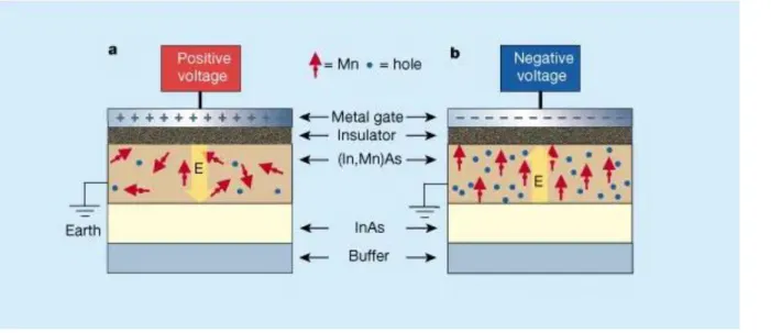
Electrical manipulation of magnetic properties was first investigated in thin films of (In,Mn)As ferromagnetic semiconductor used as channel material in the field effect transistor (FET) structure [27]. The anomalous Hall effect (AHE) has been employed to extract the magnetic modulation of the material after the application of electric field. Fig. 1.5 represents the carrier dependent spin orientations of Mn ions at different applied external gate voltages. However, direct magnetometry of magnetization modulation by external applied gate voltages was first observed in (Ga,Mn)As thin films [28]. In these materials, the Mn2+ ions not only provide local magnetic moment
but also an itinerant hole acceptor. Ferromagnetic interaction between the localized magnetic moments is mediated by the valence band holes in the framework of Zener’s p-d exchange mechanism. Following these breakthroughs, researchers started intensive work to find such type impact on metals. The first success was observed in the case of FePt and FePd thin layers by using an electric double layer transistor (EDLT) structure [29]. The large electric field generated in the EDLT structure induced surface charges that control the coercivity at room temperature. This work has changed the concept that electric field control is not possible due to the short screening length. Later, theoretical works explained that the electric field effect on surface magnetization and surface magneto crystalline anisotropy can be sufficient enough for ferromagnetic metals such as, Fe, Ni and Co due to the spin-dependent screening of the electric field. These works inspired to observe electric field effects on different materials systems
18
including Fe (Co)/Mg system where the modulation of interface anisotropy has identified as the origin. The electric field induced room temperature ferromagnetism was reported for the magnetic oxide semiconductor, (Ti,Co)O2.
From the prospective of fundamental and technological aspects, controlling magnetic properties by external means without changing temperature is of high demand. The observation of electric controlled magnetic properties of magnetic semiconductors and of magnetic metals has widen the way for the emergence of electric field controlled Spintronics devices, whose operation scheme is compatible with existing semiconductor technology.
Figure 1.5: An electrically controlled magnetic switch device structure consisting of the (In,Mn)As thin
film as channel layer in the field effect transistor (FET) structure. (a) Effect of positive gate voltage (b)
negative gate voltage on the magnetic properties of (In,Mn)As thin film [27].
1.1.5 Purpose of the present study
In this research study, we want to investigate the effect of nitrogen acceptor co-doping and electric field on the magnetism of (Zn,Fe)Te thin films. Among various II-VI DMSs, Fe-doped selenides or tellurides have been known to produce van-Vleck type paramagnetism [30, 31]. The magnetic properties of Fe based DMS are originated from the nonzero orbital momentum of Fe2+ ions having 3d6 configuration (S = 2 and L = 2). The tetrahedral crystal
field and the spin-orbit interaction induce a magnetically inactive singlet ground state, separated from higher lying excited states with energies in the range of 10-30 K, showing van-Vleck paramagnetism at low temperatures (the susceptibility is constant). However, in the presence of external magnetic field, the singlet ground state is mixed with other excited states, inducing a nonzero magnetic moment which is termed as magnetic field induced paramagnetism. This was also confirmed in the previous experimental works on Zn1-xFexTe thin films grown
under different growth conditions in our laboratory; the pure dilute phase of magnetism was observed for Fe composition, x ≤ 0.02 and the isoelectronic Fe2+ state on the substitutional site of II-VI compounds produced only
19
In the case of II-VI DMSs, the exchange interaction between the delocalized electrons (s-like) and localized electrons (d or f) is found to be independent of the host lattice or the magnetic ion. On the other hand, the exchange interaction between the delocalized holes (p-like) and the localized electrons (d or f) for all DMSs with Mn, Fe and Co is antiferromagnetic and that for Cr-based DMSs is found to be ferromagnetic. The p-d exchange is strongly based on the energy separation between the p and d states and on the degree of hybridization between the p and d wavefunctions.
However, it is suggested that the charge state and resulting spin of Fe are crucial in calculating the potential ferromagnetic coupling. The valence state change of Fe requires a d-electron to move from the Fe impurity band to one of the bands of the host semiconductor matrix or vice versa. The energy needed in this charge transfer process can be identified with the presence of donor or acceptor levels in the band gap of the host semiconductor. According to the previous research of Fe on ZnTe, the Fe 2+ / 3+ donor level is observed to be located at 150 meV above the top
of the valence band of ZnTe known from electron paramagnetic resonance (EPR) and photoconductivity measurements [34, 35]. Fig. 1.6 (a) has shown the different charge transfer levels in II-VI based semiconductor compounds and Fig. 1.6 (b) has shown the specific energetic value of donor and acceptor levels of Fe in ZnTe.
The key noting point about most DMSs is that the charge state of the magnetic ions and hence the corresponding interaction energy depends on the position of the Fermi level with respect to the band edges of the host semiconductor. Therefore, for DMSs in which the 3d impurity levels of TMs reside in the band gap, the Fermi level engineering by external charge co-doping, electric field or light are the most efficient approach to modify the magnetic properties. In the case of co-doping by external impurities, the 3d impurity levels in the band gap region can trap the carriers introduced by donor or acceptor impurities and hence, alter the charge state of magnetic ions. This deviation in valence state in turns, can modify the chemical and spin-dependent interaction between the magnetic ions. As typical examples, we can consider (Zn,Cr)Te and (Ga,Fe)N thin films, in which remarkable changes in ferromagnetic properties on co-doping with shallow impurities were reported [9, 24].
In this study, we have used nitrogen as acceptor impurity. The binding energy of N at infinite dilution deduced from Hall measurements and photoluminescence spectra is 53.4 ± 1 meV [36]. It is also known that, the maximum doping concentration of N, p ≈ 1020 cm-3 was achieved for ZnTe. Thus, it is clear that the donor levels of Fe are
situated just above the acceptor levels of N in the ZnTe matrix. However, the trap of carriers introduced by additional charge doping is expected to deviate the Fe charge state from Fe2+, resulting in a possible modification
of magnetic properties. Therefore, we are motivated to investigate how the co-doping of acceptor impurity N affects the magnetic properties of Fe-doped ZnTe, which has not yet been experimentally studied. The schematic diagram for the (Zn,Fe)Te: N study is shown in Fig. 1.7.
We have also prepared field effect transistor device structures consisting of the (Zn,Fe)Te channel layer and Al2O3 thin films / liquid electrolyte as insulating layer to modulate the magnetic properties of (Zn,Fe)Te thin films
which exhibit van-Vleck type paramagnetic behavior. In this case, our intension is that the effect of external electric field may change the valence state of Fe from Fe2+ and hence, can impact on its magnetic properties.
20
Figure 1.6: (a) Charge transfer levels Fe
2+/1+, Fe
3+/2+and Fe
3+/4+in II-VI semiconductor compounds. (b)
Energetic positions of the donor level Fe
3+/2+and acceptor level Fe
2+/1+of Fe in ZnTe [35, 37].
(a)
21
Figure 1.7: Schematic view of the N acceptor co-doped (Zn,Fe)Te research
E
Fe 3d electrons
Up
Down
Electron
Hole
Fe
2+
in ZnTe
Up
Down
N Impurity band
E
Fe
3+
in ZnTe
V. B.
V. B.
C. B.
C. B.
22
Chapter 2: Basic physical properties and previous research
2.1 The physical properties of II-VI semiconductor compound: ZnTe
Group II-VI family semiconductor compounds consist of group II B elements such as, zinc Zn, cadmium Cd, mercury Hg and group VI B family elements such as, sulphur S, selenium Se, tellurium, Te) in the atomic ratio of 1:1. Due to their excellent material properties such as optical and electrical properties, these wide band gap materials are widely used in photovoltaic conversion and optoelectronic applications. Among them, ZnTe has a direct band gap of 2.26 eV at room temperature [38]. This band gap energy belongs to the category of green region in the electromagnetic spectra. Therefore, ZnTe is a promising material for the construction of green light emitting diodes. It also finds application in THz emitters, detectors and photodetectors [39]. In fact, one of the prominent applications of ZnTe includes the photo detection in the visible region. In the present study, we will deal with II-VI semiconductor compound, ZnTe having a cubic (zinc blende: ZB) crystal structure.
2.1.1 Energy band structure
Figure 2.1 shows the energy band diagram of ZnTe. From the energy band diagram, it is observed that the conduction band minimum (CBM) and valence band maximum (VBM) has occurred at the same point (Г- point) in k-space. This is a characteristics of a direct band gap semiconductor. In such case, the electric dipole transition from VBM to CBM is allowed and the electron-hole pairs can combine radiatively with a high probability. This is why, ZnTe is a potential candidate for lasers, light emitting diodes (LEDs) and other photonic devices. Basically, ZnTe has anion p-type character with minor contribution from Zn [40].
23
2.1.2 Crystal structure of ZnTe
Each element of group II-VI semiconductor compounds has four valence electrons per atom and is in tetrahedral co-ordination. This tetrahedral geometry can be either of zinc-blende (ZB) or of wurtzite crystal structure depending on the arrangement of the neighbouring atoms. Several II-VI semiconductor compounds including ZnTe used in this study has zinc-blende crystal structure. Fig. 2.1.2 shows the crystal structure of ZnTe. It has face centred cubic structure along [111] direction. The Zn atom is located at the origin and the Te atom is located at (¼, ¼, ¼). Each Zn atom is surrounded by four Te atoms and in turn each Te atom is surrounded by zinc atoms which are also disposed towards the corner of a regular tetrahedron. We may say that the cations and anions are in equivalent position and the co-ordination of ZB structure is described as 4:4. The space group is F4̅ 3m. The
volume of the unit cell id directly related to lattice constant, a. The nearest-neighbour atomic distance is
(√3 /4) a and the lattice constant is 6.1037Å. In Fig. 2.1.2, Zn atoms are represented by blue circles and
Te atoms by red circles.
Figure 2.1.2: Crystal structure of ZnTe (Zinc-blende structure)
2.1.3 Previous research on nitrogen (N) acceptor doped ZnTe
The ab initio electronic band structure calculations for ZnO, ZnS and ZnTe crystals depending on the local-density approximation (LDA) treatment of electronic exchange and correlations and on the augmented spherical wave (ASW) for the solution of effective single-particle equations are shown in Fig. 2.1.3 [42]. For a hole to reside in the unfilled orbital of an atom, the reduction of energy due to the ionic and electronic polarization is given by
∆𝐸 = −
𝑒2
8𝜋𝑟𝜀0(1− 𝜀𝑠1)
24
25
Where r stands for the bond length, ε
s represents the static dielectric constant o the solid.By considering εs include contributions from both the ionic and electronic effects, the lowering energy
associated with ionic polarization is given by,
∆𝐸
𝑖𝑜𝑛= −
𝑒2
8𝜋𝑟𝜀0(𝜀𝑜𝑝𝑡1 − 𝜀𝑠1)
(2.1.2)
Equation (2.1.2) suggests that localization of holes is determined by a large difference between εs and εopt. It
should be mentioned that equation (2.1.2) provides an estimation of the ionic relaxation energy.
By taking the difference in electronegativity between the Zn atoms and the group VI elements into account, ΔEion is found as, ZnO (0.49 eV), ZnS (0.30 eV) and ZnTe (0.15 eV). This shows that ZnO has fair degree of of
ionic character.
At high doping levels, the impurity band is formed due to the overlapping of the acceptor orbitals which will enhance the delocalization of holes by decreasing the bandwidth of the impurity band, W to half. So, the condition for the delocalization of holes can be written as,
𝑊
2
= |∆𝐸
𝑖𝑜𝑛|
(2.1.3)From Fig, 2.1.3, the sharp DOS peaks which stands for the bonding states between the p-states at the N-site and p-states at the neighbouring Zn-sites, it is observed that the sharp DOS peak for ZnO and ZnS are position at around -0.1 eV from the Fermi energy level position because of strong repulsive potentials, while that for the ZnTe is situated at about -0.6 eV from the Fermi energy level due to the weak repulsive potentials. For ZnTe:N, the calculated N-impurity band width, W is found around 1.7 eV which is larger than twice the energy for the ionic-polarization. Thus, we can ascertain that the p-type doping of N in ZnTe will delocalize holes at higher doping concentrations.
However, for the application point of view, the N-acceptor doped ZnTe epitaxial layer showing low resistivity is needed to be grown by molecular beam epitaxy (MBE). At the beginning, it was not possible to get the physical incorporation of the dopant species because of the low sticking co-efficient. After the extensive works for more than a decade, it has now become possible to dope N in ZnTe by using both radio frequency (rf) plasma source and direct current (DC) glow plasma source [43, 44]. It is now known that hole density as high as 1020 cm-3 is
achievable by N-doping on ZnTe. The large incorporation of N atoms (≈ 1019 cm-3) in the Te-site in ZnTe crystal
can induce a significant change in the lattice parameter as shown in Fig. 2.1.4 [45]. The relative change of the lattice parameter for an epitaxial layer with [NTe] = 1019 cm-3 is given by:
26
(
∆𝑎 𝑎)
𝑍𝑛𝑇𝑒:𝑁=
𝛿𝑑 𝑑𝑍𝑛−𝑇𝑒 [𝑁𝑇𝑒] [𝑇𝑒]𝑍𝑛𝑇𝑒 (2.1.4)Where, dZn-Te = 2.62 Å, is the bond length between Zn and Te in ZnTe, [Te]ZnTe represents the concentration of
Te atoms.
If we consider one N atom (ionic radius = 0.7 Å) substitutes on Te atom (ionic radius = 1.32 Å) in ZnTe, then the difference in local bond length, ẟd = -0.62 Å and the change lattice parameter calculated from equation (4) will be -1.3 × 10⁻⁴.
Figure 2.1.4: XRD rocking curves showing the Bragg angle (004) for a 59 period ZnTe:N/ZnTe
pseudo-superlattice (SL). The two satellite peaks indicate the periodic structure of the pseudo-SL [45].
The XRD pattern of the superlattice (SL) for the (004) reflection is found to be sensitive to the lattice parameter changes as seen from the Fig. 2.2.4. A 59 period pseudo-SL where each period includes 25ML from both undoped ZnTe and ZnTe:N was grown on ZnTe (001) substrate. The zeroth order lines from the substrate and the pseudo-SL are clearly discernible. The main distinguishable feature that confirmed the presence of two epitaxial layers with different lattice parameters is two satellite peaks (m = ± 1).
Fig. 2.1.5 shows the optical spectroscopy of ZnTe:N layer at low temperature which is an essential tool to characterize dopants in the epitaxially grown layer by MBE. The Pl spectra of Undoped Zn Te layer has the dominant A°X line (exciton bound to a residual neutral acceptor), While that of the N-doped ZnTe contains the D°A° (neutral donor-acceptor pair recombination) or the e A° (conduction band electron-neutral acceptor recombination) emissions. Depending on the excitation power and the sample temperature, these D°A° and e A°
XRD angle (degree)
D
if
fr
ac
ti
on
i
n
te
n
si
ty (a. u
.)
27
bands provides the ionization energy of the acceptor. In this study, the binding energy of N for the ZnTe:N layer was found to be 53.7 ± 0.7 meV. The reflectivity measurements of the ZnTe:N (≈ 3000 Å) layer grown by homoepitaxy on ZnTe (001) substrate for N concentrations of 2 × 1018 cm-3 clearly show the splitting of the light
and heavy hole exciton lines. These are represented by E1h (light exciton) and Ehh (heavy exciton) in the reflectivity
spectra of ZnTe:N as shown in Fig. 2.2.5. These splitting suggests the presence of compressive strain in the layer. The ZnTe (001) substrate spectra is inverted after the growing of ZnTe:N layer.
Figure 2.1.5: (a) Reflectivity spectra of ZnTe (001) substrate and ZnTe:N homoepitaxial grown layer at
1.8 K. (b) Clear indication of the presence of light exciton (E
1h) and heavy exciton (E
hh) in the ZnTe:N
28
The electrical properties of a N-doped ZnTe layer grown at substrate temperature of 275°C as a
function of temperature is shown in Fig. 2.2.6. It is observed that the hole concentration and mobility has
influenced very little with the variation of temperature. This gives the clue that the transport is
accomplished by the formation of impurity band due to the overlapping of impurity wavefunctions. For
N concentration of the order of 10
19cm
-3, the atomic spacing between impurity atoms becomes of the
order of Bohr radius for hydrogenic acceptor.
Figure 2.2.6: The hole concentration and mobility as a function of Temperature [46]
2.2 The physical properties of Zn
1-xFe
xTe DMS
2.2.1 Theoretical study for the electronic structure of Fe
2+in Zn
1-x
Fe
xTe
The tetrahedrally coordinated transition metal (TM) doped II-VI DMSs has been the field of extensive research to the scientific community due to their excellent magnetic and magneto-optical properties [47]. The sp-d exchange interaction between the 3d electrons of TM impurity and the sp electrons of the host semiconductor has been the key factor in explaining various exciting phenomena in DMSs such as, large excitonic Zeeman effect, the associated Faraday and Voigt effects and the spin-flip Raman shifts of donor bound electrons [48, 49]. The thermal average of the magnetic moments of the TM impurities is maintained by macroscopic mechanisms such as crystal-
H
ol
e
c
on
c
e
n
tr
ati
on
(c
m
-3)
Temperature (K)
M
ob
il
ity
(c
m
2/V
-S
e
c
)
29
Figure 2.2.1: Energy levels of Fe
2+ion in tetrahedral crystal field, H
CF(T
d) under the effects of
spin-orbit interaction (H
SO) and Zeeman (H
Z) splitting. The energy values for the Fe
2+were determined by
numerical calculations [50].
field effect, spin-orbit interaction, static and dynamic Jahn-Teller effects, etc. Based on these mechanisms, various magnetic behavior has been proposed for different transition metal doped DMSs. For example, Mn2+ DMSs do
not affect by the crystal field splitting and exhibit “atomic like” ground state, 6S
5/2 having effective spin of (5/2) ℏ.
30
semiconductor compounds has a ground state of effective spin 3/2 due to the crystal field and spin-orbit effects. The case of Fe2+ is comparatively different from the above-mentioned cases. Fig. 2.2.1 explains the energy level
splitting of Fe2+ ion in the presence of crystal field, spin-orbit interaction and external magnetic field. For Fe2+
ion, the
5D (orbital angular momentum, L = 2, spin angular momentum, S = 2) ground states undergoes
splitting into orbital doublet,
5Г
3and an orbital triplet,
5Г
5under the influence of the tetrahedral crystal
field, H
CF(T
d). These two terms are separated by an energy gap, Δ = 4000K. Spin-orbit interaction, ℌ
SO= λ L.S gives the structure consisting of nonmagnetic singlet ground state, Г
1and several higher lying
magnetic excites states which are separated by energy gap of the order of 20K from the ground state. At
low temperatures, only the nonmagnetic ground state is occupied, providing no net magnetic moment.
However, in the presence of external magnetic field H, the Zeeman interaction, ℌ
Z= μ
BB.(L + 2S) mixes
the ground state, Г
1with the higher lying excited states to induce a magnetic moment in the direction of
the externally applied magnetic field, H. This is known as van-Vleck paramagnetic behavior [50].
2.2.2 Theoretical study for the stability of ferromagnetic state and chemical trend in Zn
1-xFe
xTe
In DMSs, it is well known that the TM ions are usually randomly substituted on the cation-site. Fig. 2.2.2 shows the theoretically calculated stabilized state for TM (V, Cr, Mn, Fe, Co and Ni) doped ZnTe semiconductor compound based DMSs [10]. In the Korringa-Kohn- Rostoker coherent potential approximation (KKR-CPA) method, the concept of disordered local moment (DLM) is normally used to describe paramagnetic state at finite temperature. On the basis of KKR-CPA method, the total energy difference between the between the DLM state and the ferromagnetic state is used to identify the stable magnetic states in these magnetic semiconductors. The positive energy difference reflects the stable state as ferromagnetic, While the negative value indicates the stable state as paramagnetic. As observed, for Mn-doped ZnTe, the spin-glass state (paramagnetic) is more stable, while for Cr and V doped ZnTe, the ferromagnetic state is more stable than the paramagnetic state. Lastly, for Fe, Co and Ni doped ZnTe, the ferromagnetic state becomes stable as the atomic number of the TM increases, but the paramagnetic state is still found to be stable in these cases.
Figure 2.2.2: Calculated total energy difference between the spin-glass (paramagnetic) states and the
31
In order to explain the magnetic structures in DMSs, the calculation of total spin polarized electron density of states (EDOS) is an important tool. Fig. 2.2.3 shows the EDOS for the model samples of TM doped ZnTe semiconductor compound based DMSs for TM composition of 3.125% [51]. This shows significant difference in the calculated EDOS for different TM doped ZnTe DMSs. Remarkable spin polarized EDOS for one spin channel and zero EDOS for other spin channel has observed for V, Cr, Fe and Ni-doped ZnTe. However, for V and Cr, the Fermi level resides on the majority spin states, While for Fe and Ni, the Fermi level reside on the minority spin
![Figure 2.2.6: The hole concentration and mobility as a function of Temperature [46]](https://thumb-ap.123doks.com/thumbv2/123deta/8498613.922905/29.918.166.788.318.733/figure-hole-concentration-mobility-function-temperature.webp)
![Figure 2.2.7: XANES spectra of Zn 1-x Fe x Te thin films with different Fe composition grown under Te- rich condition [32]](https://thumb-ap.123doks.com/thumbv2/123deta/8498613.922905/37.918.104.682.278.1005/figure-xanes-spectra-films-different-composition-grown-condition.webp)
![Figure 2.2.10: M-H curves for Zn 1-x Fe x Te thin films with different Fe composition grown under Te-rich condition [32]](https://thumb-ap.123doks.com/thumbv2/123deta/8498613.922905/40.918.112.825.161.577/figure-curves-films-different-composition-grown-rich-condition.webp)
![Figure 2.2.16: M-T curves for Zn 1-x Fe x Te thin films with different Fe composition grown under Zn-rich condition [33]](https://thumb-ap.123doks.com/thumbv2/123deta/8498613.922905/45.918.111.833.435.995/figure-curves-films-different-composition-grown-rich-condition.webp)
![Figure 2.3.1: Schematic representation of the microscopic reduction mechanism of the intra-atomic Coulomb repulsion energy of 3d TM impurity atom (a) in isolated condition and (b) in semiconductors [13]](https://thumb-ap.123doks.com/thumbv2/123deta/8498613.922905/46.918.137.828.643.993/schematic-representation-microscopic-reduction-mechanism-repulsion-condition-semiconductors.webp)
![Figure 2.4.2: EDS mapping showing Cr distribution in Zn 1-x Cr x Te thin films with Cr composition, x = 5% grown under (a) Te-rich growth condition (b) Zn-rich growth condition [9]](https://thumb-ap.123doks.com/thumbv2/123deta/8498613.922905/49.918.169.828.274.562/figure-mapping-showing-distribution-composition-condition-growth-condition.webp)
![Figure 2.4.14: M-H curve of the undoped, I-doped and N-doped Zn 1-x Cr x Te thin films with Cr composition, x = 5% and I concentration, [I] = 2 × 10 18 cm -3 and N concentration, [N] = 5 × 10 20 cm -3](https://thumb-ap.123doks.com/thumbv2/123deta/8498613.922905/59.918.178.829.299.760/figure-curve-undoped-doped-films-composition-concentration-concentration.webp)
![Figure 2.4.17: Comparison of Cr distributions in Zn 1-x Cr x Te thin films with Cr composition, x = 5% and different I concentrations (a) [I] = 1 × 10 19 cm -3 (b) [I] = 2 × 10 18 cm -3 and (c) [I] < 1 × 10 17 cm -3 [9]](https://thumb-ap.123doks.com/thumbv2/123deta/8498613.922905/61.918.132.828.774.1003/figure-comparison-distributions-cr-films-composition-different-concentrations.webp)
