Dependable Dual Edge Triggered Flip-Flops for Bloking Noise Signal
Yukiya Miura †
Abstract
This paper proposes a dual edge triggered flip-flop for blocking a noise signal induced on data signal lines. The clock signal has two edges in nature, the rising edge and the falling edge. If an edge triggered flip-flop can sample data by using those two edges during one clock period, the flip-flop has the highly ability to prevent sampling the noise signal on the data line, comparing the conventional single edge triggered flip-flops. The proposed flip-flops have advantages that they do not require any additional clock/control signal and delay element to block the noise signal. Thus, their implementation/application to existing synchronous digital circuits is easy. Besides, the noise width that the proposed flip-flops can block is adjustable when the width of the clock signal is adjustable. In addition to noise signal blocking, they can apply to detection/correction of timing errors and delay faults. We show effectiveness of proposed design by circuit simulation.
Keywords: data signal, dependable design, edge
triggered flip-flop, noise, single event transient, synchronous circuits
1. Introduction
According to scale-down of devise dimensions, reduction of a power supply voltage and speed-up of an operation speed by CMOS technology development, signal noises induced by energetic particles (e.g., soft errors) and by signal changes (e.g., crosstalk) come to influence circuit behaviors. For DSM VLSIs, errors by a single event transient (SET) become a serious problem as well as a single event upset [1]. The width of a SET pulse becomes wider, pulse propagation in the circuit becomes easy, and the pulse is sampled easy by flip-flops (FFs) as the operational frequency is higher. In addition, single event (SE) (e.g., single event transient) causes a crosstalk noise [2]. This effect is noticeable as the power supply voltage is lower, and the width of the crosstalk pulse increases as the power supply voltage is lower.
Since those signal noises caused by SE and internal signal changes are transient signal/voltage pulses, the circuit often results in a transient fault when the noise is sampled by FFs [3], [4]. Thus, in this paper, we focus the voltage pulse induced on the data signal line by multisource noise effects (e.g., SET and crosstalk), because we have already proposed noise blocking methods for the noise pulse on the clock signal line [5]. In order to prevent erroneous data sampled by FFs, several techniques have been proposed.
(1) Multiple data sampling method [3], [6]-[8]: In those method, two or more FFs sample data. The double data sampling method is a time and space redundancy method by using two FFs and two sampling times. If contents of two FFs are not consistent, the method produces an error signal. This method can detect error occurrence by on-line, but cannot correct it. The Razor method and the canary FF method are ones derived from this method [9], [10].
(2) Multiple redundancy method [11], [12]: In those method, dual modular redundancy or triple modular redundancy techniques are used to compare values in FFs. Those methods can block the glitch on the data line, but require additional control/clock signals. (3) Noise reduction method [1], [13], [14]: In those
methods, the amplitude of the noise signal is reduced by a masking/filtering effect. The reduction ratio depends on the value of RC product and the hysteresis property of the Schmitt trigger circuit. They may have the problem of the signal propagation speed, power consumption, and area overhead. In addition, their efficiency is unknown for the large pulse.
In this paper, a dependable edge triggered FF based on a new concept is proposed, which can block the transient voltage pulse on the data signal line, and results in dependable design. The clock signal has two edges in one period, the rising edge and the falling edge. If data samplings are carried out at both the rising edge and the falling edge, the transient pulse occurred at a single edge is never sampled and such the ET-FF can block the noise signal. We call such ET-FF a dual edge triggered flip-flop (DET-FF). The DET-FF does not require any additional clock/control signals and the noise width that the DET-FF can block is adjustable.
The rest of the paper is organized as follows. Section 2 introduces the purpose of this paper. The dual edge triggered flip-flop is presented in Section 3. Section 4 presents an implementation example of the DET-FF. We show the effectiveness of the proposed method through simulation results and describe observations for simulation results in Section 5. Finally, we conclude this work in Section 6.
2. Purpose
In this paper, we focus edge triggered flip-flops (ET-FFs) and transient voltage pulses on the data signal line induced by several noise sources (e.g., SET and crosstalk). We aim to prevent to sample such transient pulse as proper data by ET-FFs.
Signal noise and signal integrity problems are becoming one of serious issues for quality of DSM VLSI circuits. Signal noise will happen accidentally at any location, and will cause a transient voltage pulse on data lines. Prediction and prevention of signal noise occurrence is difficult, because noise sources exist outside and inside of a VLSI chip and we usually do not have any way for calculating and solving their occurrence in VLSIs. We consider that signal noise will happen without intention and the prevention of influence caused by the noise in the circuit level is one of reasonable solutions for the measure against signal noise.
Conventional ET-FFs use only one edge, either the rising edge or the falling edge to sample data, but not both. If the transient noise signal occurs on the data signal line and the signal occurrence satisfies the time constrains of the setup time and the hold time at the rising edge or the falling edge, the conventional ET-FF samples the noise signal as a proper data signal and it finally holds and outputs an erroneous value.
If we use multiple data samplings to catch proper data, we can evaluate the width of the signal pulse (i.e., the signal having enough duration time (width), not the glitch). The clock signal has two edges (i.e., the rising edge and the falling edge) into one period in nature. If data samplings are carried out at both the rising edge and the falling edge, the transient pulse occurred at the single edge is never sampled and such the ET-FF can block the noise signal. We call such ET-FF the dual edge triggered flip-flop (DET-FF). The DET-FF does not require any additional clock/control signal, any delayed element, and any explicit duplication circuit. In addition, the noise width that the DET-FF can block is adjustable when the width of the clock signal is adjustable. Thus, by using the nature of the clock signal, the DET-FF can block to sample/hold erroneous data caused by transient signal noises.
Note that FFs called the double-edge triggered FF and the dual-edge triggered FF have been proposed [15]-[18]. Conventional ET-FF samples/holds data synchronizing the single edge either the rising edge or the falling edge. On the other hand, those FFs use both edges to sample/hold each data signal, and then they can operate at half the clock frequency of conventional single ET-FFs. As a result, the method can reduce the power consumption. Therefore, this is a quite different technique with proposed dependable FFs.
3. Dual edge triggered flip-flops
In the following, for simple discussion, we consider that the clock signal and the noise pulse are the positive type and the data signal is positive logic (i.e., the active high level). The proposed method is applicable for every combination of negative logic and positive logic between the clock signal and the noise pulse. In this paper, we also consider the noise pulse of a rectangle wave form for simple discussion.
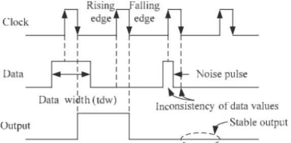
The proposed DET-FF samples data by using both the rising edge and the falling edge. If a data signal width is wider than the clock pulse width including the setup and hold times, the signal is proper data and the DET-FF samples/holds its value (Fig. 1, left). If the width of the data signal is narrow than the interval between both edges, the DET-FF recognizes that the signal is noise because of inconsistency of data values at both edges (Fig. 1, right). The DET-FF does not sample the signal and its output holds the previous value. Therefore, the DET-FF can block the noise pulse. This method has advantages that any additional signals are not needed and the width of the noise pulse we wish to block is adjustable if the timing of the rising edge or the falling edge is changed.
The width of the data signal, tdw, must satisfy the timing constraint as follows:
Conventional ET-FF: tdw ≥ tsu + th, Proposed DET-FF: tdw ≥ tsu + th + tw,
where tsu and th are the setup time and the hold time, and
tw is the width of the clock pulse (Fig. 2). Thus the data
duration time of the DET-FF becomes longer than that of the conventional ET-FF. This may be drawback of the proposed method.
Figure 1 Concept of dual edge triggered flip-flop.
Figure 2 Setup time and hold time.
4. Implementation
In order to implement the DET-FF as a realization example, we use first stage circuits of conventional ET-FFs because they have good characteristics as an edge detector. The second stage of the conventional ET-FF is the SR-FF. The left side of Fig. 3 is the conventional positive (rising) ET-FF and the right one is the first stage of the conventional negative (falling) FF. In the positive ET-FF, when C=0, the first stage samples data, then, QMB=DB, QM=D. Here VB denotes the inversion of a logic value V. At this time, the second stage holds the previous state. When C goes to the logic 1 (0 −> 1), values
of QMB and QM propagate respectively to Ep and EpB through inversion gates, then Ep=D and EpB=DB, and the FF holds/outputs the sampled values. This condition continues until next rising edge of C. For the other combinations of (C, D), the FF holds the previous value. Note that (Ep, EpB)=(0, 0) never occurs because of specification of the SR-FF. The negative ET-FF operates in the similar way except for clock conditions.
Figure 4 shows state transition diagrams of the first stages of conventional ET-FFs. The difference of these two circuits is the clock transition direction only, and the other behaviors are the same each other. When the transitions of two bold solid lines or two bold dashed lines occur sequentially, both circuits sample the same value at the rising and falling edges. At this time, sampled data is proper data. For the other transitions, the circuit holds the previous value.
Now consider the relationship between the clock signal and the data signal. Considering the function of the DET-FF, there are four states for the relationship as shown in Fig. 5. In the proposed DET-FF, when the data signal at the rising edge is the same as the data signal at the falling edge (states (1) and (2) in Fig. 5), it is the proper signal. Then the DET-FF holds and outputs the signal. On the other hand, when the data signals at both edges are different each other (states (3) and (4)), the DET-FF recognizes that the noise signal comes to the FF input and the DET-FF must hold the previous value.
Table 1 summarizes the function of the DET-FF. States (1) and (2) are the cases of proper data, and then the DET-FF holds/outputs the value of D reached at the DET-FF input. If the noise pulse reaches to the FF input (states (3) and (4)), the DET-FF holds the output value of the previous state. At this time, a warning signal plays the role of a flag to inform that the data signal at the rising edge is different from one at the falling edge. Its usage is explained later. For the other clock conditions (the last three rows in the table), the FF itself is in the hold state (state (Hold)), whose function is similar to conventional ET-FFs. Note that since the second stage (i.e., output state) of the conventional ET-FF is the SR-FF, (Ep, EpB)=(0, 0) and (En, EnB)=(1, 1) never occur.
Implementation example of a circuit satisfying the above function is shown in Figs. 6 and 7. The first stages of the conventional ET-FFs are the same as circuits shown in Fig. 3, which have the function to sample data at the clock edge. The second stage circuits are designed for satisfying the function of Table 1.
The DET-FF firstly samples data at the rising edge, and its value must be temporarily held until data is sampled at the following falling edge. In order to realize this function, the proposed DET-FF uses the two-input Muller C-element for the output stage of the rising edge part. The DET-FF must hold the previous value if the data value sampled by the falling edge is different from that of the temporary holding value (i.e., the data value sampled by the rising
edge). In addition, The FF must check whether those two values are the same or not comparing each other. In order to realize this function, the DET-FF uses the three-input Muller C-element for the output stage of the FF.
Figure 3 Conventional edge triggered flip-flops.
1,1 0,1 1,0 (0,X)/Q (C,D)/Q (1,0)/0 (0,X)/Q (0,X)/Q (1,1)/1 (1,X)/0 (1,X)/1 State:Ep,EpB 0,0 0,1 1,0 (1,X)/Q (C,D)/Q (0,0)/0 (1,X)/Q (1,X)/Q (0,1)/1 (0,X)/0 (0,X)/1 State:En,EnB
Figure 4 State transition diagrams of first stages of conventional edge triggered flip-flops.
Figure 5 Relationship between clock and data signals. Table 1 Function table of dual edge triggered flip-flop.
State Warning
C D Ep, EpB C D En,EnB Q QB (1) 1 1, 0 1 1, 0 1 0 0 (2) 0 0, 1 0 0, 1 0 1 0 (3) 1 1, 0 0 0, 1 1 (4) 0 0, 1 1 1, 0 1 (Hold) X 1, 1 X 0, 0 0 (Hold) 0 X 1, 1 1 X 0, 0 0 (Hold) 1 X D0, DB0 0 X D0, DB0 0 No change No change Note: (Ep, EpB)=(0, 0) and (En, EnB)=(1, 1) do not exist.
D0and DB0denote previous values when C=1 (positive FF) or C=0 (negative FF).
1st edge 2nd edge Output
No change No change No change
The part enclosed with the dashed line of Fig. 6 temporarily holds the value sampled by the rising edge at the node Q1. The three-input C-element at the final stage has two functions. It firstly compares the temporarily
holding value with the value sampled by the following falling edge (i.e., a pair of (En, EnB)). Based on the comparison result of consistency/inconsistency of two values, the DET-FF outputs either the new sampled value or previous value.
Figure 6 Dual edge triggered flip-flop. VDD S1 En S2 Q1 S1 GND S3 En Q1 S3 EnB EnB S2 En S3 Warning
Figure 7 Warning circuit of dual edge triggered flip-flop. Until here, we assume the positive clock pulse. Exchanging (Ep, EpB) and (En, EnB), the circuit of Fig. 6 is applicable for the negative clock pulse.
A warning circuit of Fig. 7 informs us that there is the noise pulse (i.e., the value at the rising edge is different from one at the falling edge) producing the high level
output. At this time, we know that the output of the DET-FF is the previous value because of blocking the noise pulse. This function is realized by the combination of Q1, En, EnB and their inversion signals. The warning circuit can function for both the positive clock pulse and the negative clock pulse.
5. Evaluation
The functions of Figs. 6 and 7 are verified by using 1.8 V 0.18-m TSMC parameters. Figure 8 shows simulation results, where from the top, the figure shows the clock signal, the data signal, the output signals (solid line: DET-FF, dotted line: conventional positive ET-FF), and the warning output.
Data signal:
- (a) and (d): proper data signal - (b) and (c): noise signal
- The data value is the logic 1 for intervals (a) and (d), and the logic 0 for the other intervals.
FF output signal:
- The DET-FF outputs the logic 1 for intervals (a1) and (d1) that correspond to intervals (a) and (d) of the logic 1 input, and the logic 0 for the other interval including noise pulses of (b) and (c). Thus the DET-FF can block noise pulses of (b) and (c).
- The conventional positive ET-FF outputs the logic 1 for the interval (b1) responding to the noise of (b) as well as intervals of (a) and (d) of proper signals. Thus, it malfunctions because of the noise pulse.
Warning output:
- The warning circuit outputs the warning signal for the intervals of (b2) and (c2) whenever noise pulses (i.e., (b) and (c)) appear on the data line. Thus, the circuit informs us that the noise pulse appears on the data line and it is blocked, and the DET-FF is holding the previous value.
From simulation results, we find the following observations. Time 0s 2ns 4ns 6ns 8ns 10ns 12ns 14ns 16ns 18ns 20ns 22ns V(60) 1.0V -0.1V SEL>> V(50) V(20) 0V 1.0V V(11) 0V 1.0V V(10) 0V 1.0V
Figure 8 Simulation results of dual edge triggered flip-flop. Clock Data Q output Warning (a) (b) (a1) (b1) 3 1 2 4
DET-FF output Conventional ET-FF output 5 6 7 (c) (d) (d1) (c2) (b2)
(1) DET-FF size: The number of transistors of the DET-FF (Figs. 6 and 7) is 74. If the same function of the DET-FF is realized by the combination of two conventional ET-FF, it requires a comparator, a multiplexer, a keeper, and a delay element. Then the number of transistors of its transistor level circuit is approximately 70 and the delay element. Transistor count of the proposed DET-FF is almost the same as the implementation by two conventional ET-FFs, but conventional one is needed the delay element. The DET-FF in this paper uses the first stage of the conventional ET-FF, however if we newly design this part, the DET-FF should become a smaller circuit, because the first stage circuit occupies 36 transistors among total transistors of the DET-FF (i.e., 49% of the total number of transistors).
(2) DET-FF performance: Table 2 summarizes AC characteristics of the DET-FF. Depending on a noise pulse type (positive or negative) and noise pulse generation timing, the DET-FF response differs. Values of [range] in the table mean the best value and the maximum value for each item. The noise width
tnw that the DET-FF can block is determined by the
clock pulse width tw. If tw=0.351 ns, the DET-FF can block surely the noise width between 0.231 ns and 0.351 ns (+tsu+th). Since the DET-FF uses two C-elements, propagation delay is relatively large. The minimum functional period T of the DET-FF alone is calculated as follows: T=tw+tsu+max(th, tpQ, tpW)= 1.121 ns. Then, maximum operating frequency is approximately 892 MHz
(3) Noise blocking ratio: The noise blocking ratio, NBR, within one clock period of the DET-FF is calculated by using Fig. 9. Let a=tw, b=tnw, here, b=a (0<<1), 0<a<2/T for simple equations. For case 1, the DET-FF can block the noise signal around edges:
(b/T)*2 =2a/T. (1)
For cases 2 and 3, the noise signal occurring the other interval dose not influence FF function:
Table 2 AC characteristics.
max [range] positive negative minimum clock pulse width tw [ns] 0.351 - -setup time tsu [ns] 0.019 [-0.156, +0.019] 0.060 0.117 hold time th [ns] 0.191 [0.022, 0.191] 0.292 0.200 propagation delay of Q tpQ [ns] 0.493 [0.342, -0.493] 0.241 0.246 propagation delay of warning tpW [ns] 0.751 [0.241, 0.751] - -minimum noise width tnw [ns] 0.231 [0.141, 0.231] - -minimum noise amplitude Vn [V] 1.007 [0.861, 1.007] 1.009 0.901
DET-FF Conventional FF (tw) T 0 T/2 a (tnw) b
(case 1) noise block
(case 2) non-influence (case 3) non-influence b T/2-a/2-b a-b C D T/2-a/2 D D
Figure 9 Noise blocking ratio.
((T-a-b)/T)+(a-b)/T=(T-2b)/T =(T-2a)/T. (2) From equations of (1) and (2), NBR is calculated as:
NBR=(1)/(2)= 2a/(T-2a)=2b/(T-2b). (3) From (3), we find that NBR depends on the width of the noise pulse (clock pulse) if the width of the clock pulse (noise pulse) is constant.
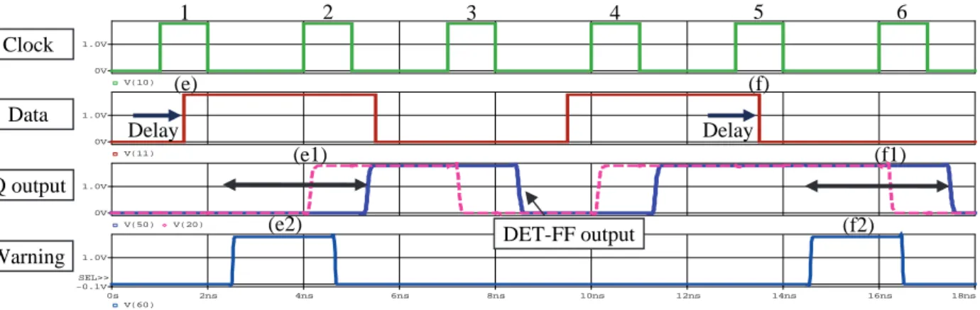
(4) DET-FF behavior (application to other error): We design the DET-FF as a noise aware technique. In addition, the proposed DET-FF can find timing violation of the data signal that results in extra delay. In the policy of DET-FF design, the data signal must arrive before the first edge of the dual-edge. Therefore,
Time 0s 2ns 4ns 6ns 8ns 10ns 12ns 14ns 16ns 18ns V(60) 1.0V -0.1V SEL>> V(50) V(20) 0V 1.0V V(11) 0V 1.0V V(10) 0V 1.0V
Figure 10 Example of timing violation of data signal. Clock Data Q output Warning (e) (e1) (e2) 1 2 (f2) 5 6 3 4 DET-FF output (f1) (f) Delay Delay
if a signal change happens between two edges of the dual-edge, there is extra delay (e.g., delay fault) or timing violence by some reasons. In this case, since signal values between the rising edge and the falling edge are different, the DET-FF can find it. Figure 10 shows those simulation results. Signal transition to the logic 1 (0) is delayed at (e) ((f)), the warning flag is outputted at (e2) ((f2)), and we find there is timing violence in the data signal. For both cases (e) and (f), the DET-FF holds the previous value, however, for (e) ((f)), it seems that the DET-FF outputs the logic 0 (1) state as an extra output of just one clock period. However, this behavior is the nature of ET-FFs, not incorrect behavior.
6. Conclusions
This paper proposed the dual edge triggered flip-flop, DET-FF, which can block the noise pulse by using two edges of the clock signal. The DET-FF informs us that there is the noise signal on the data line by outputting the warning signal and the FF holds the previous value. We verified the DET-FF function by using circuit simulation. The DET-FF does not require any additional signal and delay element. So the application of the DET-FF to existing circuits is easy. In addition to noise pulse blocking, the DET-FF can apply to detection/correction of timing errors and delay faults that mean violence of timing constraint of FFs.
For implementing the DET-FF, this paper used the first stage circuit of the conventional ET-FF. For reducing the circuit size and improving performance, an implementation method must be improved. Besides, in order to show characteristics of the DET-FF, performance evaluation (e.g., speed, area, power, and application range, and etc.) compared with other similar methods is needed. This paper considered the edge triggered FF. We will apply the similar idea to the level sensitive (master-slave) FF. In addition, a noise generation/evaluation method is needed in future works.
Acknowledgement
The author would like to thank Professor Joan Figueras of Universitat Politècnica de Catalunya for his helpful discussions and comments. This research was supported in part by Japan Society for the Promotion of Science under Grant-in-Aid for Scientific Research (C) (No. 21500059).
References
[1] D. Munteanu, and J.-L. Autran, “Modeling and simulation of single-event effects in digital devices and ICs,” IEEE Trans. Nuclear Science, vol.55, no.4, pp.1854-1878, August 2008.
[2] A. Balasubramanian, O. A. Amusan, B.L. Bhuva, R.A. Reed, A.L. Sternberg, L.W. Massengill, D. McMorrow, S.A. Nation, and J.S. Melinger, “Measurement and analysis of interconnect crosstalk due to single events in a 90 nm
CMOS technology,” IEEE Trans. Nuclear Science, vol.55, no.4, pp. 2079-2084, August 2008.
[3] S. Mitra, N. Seifert, M. Zhang, Q. Shi, and K.S. Kim, “Robust system design with built-in soft-error resilience,” IEEE Computer, vol.38, no.2. pp.43-52, February 2005.
[4] Y. Yanagawa, D. Kobayashi, H. Ikeda, H. Saito, and K. Hirose, “Scab-architecture-based evaluation technique of SET and SEU soft-error rates at each flip-flop in logic VLSI systems,” IEEE Trans. Nuclear Science, vol.55, no.4, pp. 1947-1952, August 2008.
[5] Y. Miura, “Dependable Clock Distribution for Crosstalk Aware Design,” Proc. International Test Conference, no.29.1, 2007.
[6] M. Nicolaidis, “Time redundancy based soft-error tolerance to rescue nanometer technologies,” Proc. 17th IEEE VLSI symposium, pp.89-94, 1999.
[7] J. Gambles and K.J. Hass, U.S. Patent, 6326809, 1999.
[8] N.D.P. Avirneni, V. Subramanian, and A.K. Somani, “Low overhead soft error mitigation techniques for high-performance and aggressive systems,” Proc. 39th International Conference of Dependable Systems and Networks, pp.185-194, 2009.
[9] D. Ernst, N.S. Kim, S. Das, S. Pant, R. Rao, T. Pham, C. Ziesler, D. Blaauw, T. Austin, K. Flautner, and T. Mudge, “Razor: A low-power pipeline based on circuit-level timing speculation,” Proc. 36th International Symposium on Microarchitecture, pp.7-18, 2003.
[10] T. Sato and Y. Kunitake, “A simple flip-flop circuit for typical-case designs for DFM,” Proc. 8th International Symposium on Quality Electronic Design, pp. 539-544, 2007.
[11] A. Goel, S. Bhunia, H. Mahmoodi, and K. Roy, “Low-overhead design of soft-error-tolerant scan flip-flops with snhanced-scan capability,” Proc. Asian and South Pacific Conference on Design Automation, pp.665-670, 2006.
[12] M. Chen and A. Orailoglu, “Improving circuit robustness with costeffective soft-error-tolerant sequential elements,” Proc. 16th IEEE Asian Test Symposium, pp.307-312, 2007.
[13] Y. Sasaki, K. Namba, and H.Ito, “Soft error masking circuit and latch using schmitt trigger circuit,” Proc. 21st International Symposium on Defect and Fault Tolerance in VLSI Systems, pp327-335, 2006.
[14] M.R. Choudhury, Q. Zhou, and K. Mohanram, “Soft error rate reduction using circuit optimization and transient filter insertion,” Journal Electron Testing: Theory and Applications, vol.25, pp.191-207, 2009.
[15] S.H. Unger, “Double-edge-triggered flip-flops,” IEEE Trans. Computers, vol.C-30, no.6, pp.447-451, 1981.
[16] R.Hossain, L.D. Wronski, and A. Albicki, “Low power design using double edge tiggered flip-flops,” IEEE Trans. Very Large Scale Integration systems, vol.2, no.2, pp.261-265, 1994.
[17] J. Tschanz, S. Narendra, Z. Chen, S. Borkar, M. Sachdev, and V. De, “Comparative delay and energy of single edge-triggered & dual edge-edge-triggered pulsed flip-flops for high-performance microprocessors,” Proc. International Symposium on Low Power Electronics and Design, pp.147-152, 2001.
[18] A. Ghadiri and H. Mahmoodi, “Dual-edge triggered static pulsed flip-flops,” Proc. 18th International Conference on VLSI Design, pp.846-849, 2005.