Japan Advanced Institute of Science and Technology Title
BNおよびAlTiO高誘電率ゲート絶縁体を用いた
AlGaN/GaN金属‑絶縁体‑半導体ヘテロ接合電界効果トラ ンジスタ
Author(s) Nguyen, Quy Tuan Citation
Issue Date 2014‑09
Type Thesis or Dissertation Text version ETD
URL http://hdl.handle.net/10119/12305 Rights
Description Supervisor:鈴木 寿一, マテリアルサイエンス研究科
, 博士
heterojunction field-effect transistors using BN and AlTiO high-k gate insulators
NGUYEN QUY TUAN
Japan Advanced Institute of Science and Technology
AlGaN/GaN metal-insulator-semiconductor heterojunction field-effect transistors using BN and AlTiO high-k gate insulators
NGUYEN QUY TUAN
Supervisor: Prof. Toshi-kazu SUZUKI, Ph.D.
School of Materials Science
Japan Advanced Institute of Science and Technology
September, 2014
GaN-based metal-insulator-semiconductor heterojunction field-effect transistors (MIS-HFETs) have been investigated owing to the merits of gate leakage reduction and passivation to sup- press the current collapse. Gate insulators, such as Al2O3, HfO2, TiO2, or AlN, have been studied. Further developments of the MIS-HFETs using novel gate insulators suitable ac- cording to applications are important. A desired gate insulator should have:
• wide energy gap Eg and high breakdown fieldFbr for high voltage operation,
• high dielectric constant kfor high transconductance, and
• high thermal conductivity κ for good heat release suitable for high power operation In particular, boron nitride (BN) and aluminum titanium oxide (AlTiO: an alloy of TiO2and Al2O3) are promising candidates owing to their advantageous properties, as shown below.
In this work, we characterized physical properties of amorphous BN thin films obtained by RF magnetron sputtering, which haveEg ∼5.7 eV,Fbr ∼5.5 MV/cm, andk∼7. Using the BN films, we fabricated BN/AlGaN/GaN MIS-HFETs (BN MIS-HFETs), which exhibit very low gate leakage, indicating good insulating properties of BN. We obtain high maximum drain current ID and no negative conductance, suggesting good thermal release properties owing to the excellent κ of BN. We elucidated temperature-dependent channel conduction, where ID decreases with increase in temperature. In the linear region, the decrease in ID
is attributed to decrease in the electron mobility, while the sheet electron concentration is constant. In the saturation region, the decreased ID is proportional to the average electron velocity, whose temperature dependence is in-between those of the low- and high-field ve- locities. Furthermore, we elucidated the temperature-dependent gate leakage, attributed to a mechanism with temperature-independent tunneling, dominant at low temperatures, and temperature-enhanced tunneling, dominant at high temperatures, from which we estimated the BN/AlGaN interface state density, which is≫1012cm−2eV−1. High-density BN/AlGaN interface states lead to the weak gate controllability for the BN MIS-HFETs.
We also characterized physical properties of AlxTiyO thin films obtained by atomic layer deposition, for several Al compositions x/(x+y). We observe increasing Eg and Fbr, and decreasingk with increase in the Al composition. Considering the trade-off between k and Fbr, we applied AlxTiyO with x : y = 0.73 : 0.27, where Eg ∼ 6 eV, Fbr ∼ 6.5 MV/cm, and k ∼ 24, to fabrication of AlTiO/AlGaN/GaN MIS-HFETs (AlTiO MIS-HFETs). In comparison with Al2O3/AlGaN/GaN MIS-HFETs, the AlTiO MIS-HFETs exhibit higher maximumID, higher peak and better linearity of transconductance, shallower threshold volt- age, and higher gate leakage (but still very low), suggesting that AlTiO is more favorable
i
than Al2O3 for applications to AlGaN/GaN MIS-HFETs. We investigated temperature- dependent channel conduction of the AlTiO MIS-HFETs, whereID decreases with increase in temperature. In the linear region, the decrease inID is mainly due to decrease in the elec- tron mobility, while the contact resistance and the sheet electron concentration are almost constant. In the saturation region, the decreased ID is proportional to the average electron velocity, whose temperature dependence is in-between those of the low- and high-field veloci- ties. Temperature-dependent channel conduction of the AlTiO MIS-HFETs is similar to that of the BN MIS-HFETs. Moreover, we observe bumps in gate current for high drain-source voltages and high ID, indicating increase in channel temperature due to self-heating effects at high power consumption. This suggests low κ of AlTiO due to random effects in alloy materials. In addition, we elucidated the temperature-dependent gate leakage, attributed to a mechanism with two terms. One is temperature-independent tunneling, dominant at low temperatures. The other exhibits Poole-Frenkel mechanism, dominant at high temper- atures, from which we estimated AlTiO/AlGaN interface state density, which is ∼2×1012 cm−2eV−1. Low-density AlTiO/AlGaN interface states lead to the strong gate controllability for the AlTiO MIS-HFETs.
Finally, we concluded that AlTiO films have low thermal conductivity, but low interface state density in comparison with those of BN films.
Keywords: AlGaN/GaN, MIS-HFET, BN, AlTiO, channel conduction, gate leakage, interface state
Completing my Ph.D. degree is probably the most challenging activity of my first 30 years of my life. I have received a lot of supports and encouragements from many people since I came to Japan Advanced Institute of Science and Technology (JAIST). I would like to show my great appreciation to them.
First of all, I would like to express my deep gratitude to my supervisor, Prof. Toshi- kazu Suzuki for his strong supports, constant encouragement, and whole hearted guidances.
He has been taught me a lot of things in the research, fundamental knowledge in physics, mathematics, linguistics, ... and also guided me many things in daily life. I have been lucky to have him as my mentor.
Moreover, I would like to exhibit my appreciation to Prof. Syoji Yamada for his kind support as a second supervisor, Assoc. Prof. Chi Hieu Dam for his strong support on my sub-theme research, and Assoc. Prof. Masashi Akabori for his great help and supports.
Furthermore, I highly appreciate Cong T. Nguyen for his help and advices in daily life and the research. Thanks to him for careful checking this dissertation. I would like to thank M. Kudo, T. Ui, Y. Yamamoto, N. Hashimoto, Son P. Le, and S. Hidaka for their strong and kind helps in the research and life here. Especially, many thanks to H.A. Shih for his careful and patient instructions in experimental works at my starting research works at JAIST. I also would like to thank all members of Suzuki, Yamada, and Akabori laboratories for their kind helps.
In addition, would like to thank Lam T. Pham, Cuong T. Nguyen, and my friends in the 4th batch of Vietnam National University, Hanoi - JAIST Dual Graduate Program for providing support and friendship that I needed.
Especially, I would like to express my appreciation to the 322 project of Vietnamese government for its financial supports.
Finally, I wish to thank my parents, my brothers and sister. Their love and encourage- ments provided my inspiration and was my driving force. I wish I could show them just how much I love and appreciate them.
iii
Abstract i
Acknowledgements iii
Table of Contents iv
List of Figures vi
List of Tables xii
1 Introduction 1
1.1 Trends of semiconductor industry . . . 1
1.2 GaN-based materials and devices . . . 6
1.2.1 Advantageous properties of GaN-based materials . . . 6
1.2.2 GaN-based Schottky-HFETs and MIS-HFETs . . . 13
1.3 BN and AlTiO as a high-dielectric-constant (high-k) insulator . . . 14
1.3.1 Boron nitride (BN) . . . 14
1.3.2 Aluminum titanium oxide (AlTiO) . . . 16
1.4 Purposes of this study . . . 18
1.5 Organization of the dissertation . . . 19
2 Fabrication process methods for AlGaN/GaN MIS-HFETs 20 2.1 Marker formation . . . 20
2.2 Ohmic electrode formation . . . 22
2.3 Device isolation . . . 25
2.4 Gate insulator deposition . . . 28
2.5 Gate electrode formation . . . 29
2.6 Summary of chapter 2 . . . 32
3 BN thin films and BN/AlGaN/GaN MIS-HFETs 33 3.1 Deposition and characterization of BN thin films . . . 33
3.1.1 RF magnetron sputtering deposition of BN thin films . . . 33
3.1.2 Characterization of BN thin films on n-Si(001) substrate . . . . 34
3.1.3 Characterization of BN thin films on AlGaN/GaN heterostructure . 38 3.2 Fabrication and characterization of BN/AlGaN/GaN MIS-HFETs . . . 42
3.2.1 Fabrication of BN/AlGaN/GaN MIS-HFETs (BN MIS-HFETs) . . . 42 iv
3.2.2 Effects of ambiences on BN MIS-HFET characteristics . . . 42 3.2.3 Temperature dependence of output and transfer characteristics of BN
MIS-HFETs . . . 45 3.2.4 Temperature dependence of gate leakage of BN MIS-HFETs . . . 52 3.3 Summary of chapter 3 . . . 58 4 AlTiO thin films and AlTiO/AlGaN/GaN MIS-HFETs 59 4.1 Deposition and characterization of AlTiO thin films . . . 59 4.1.1 Atomic layer deposition of AlTiO thin films . . . 59 4.1.2 Characterization of AlTiO thin films on n-GaAs(001) substrate . . . 61 4.1.3 Characterization of AlTiO thin films on AlGaN/GaN heterostructure 64 4.2 Fabrication and characterization
of AlTiO/AlGaN/GaN MIS-HFETs . . . 66 4.2.1 Fabrication of AlTiO/AlGaN/GaN MIS-HFETs (AlTiO MIS-HFETs) 66 4.2.2 Effects of annealing on gate leakage of AlTiO MIS-HFETs . . . 66 4.2.3 Advantages of AlTiO in comparison with Al2O3 . . . 67 4.2.4 Temperature dependence of output and transfer characteristics of Al-
TiO MIS-HFETs . . . 68 4.2.5 Temperature dependence of gate leakage of AlTiO MIS-HFETs . . . 77 4.3 Summary of chapter 4 . . . 84
5 Conclusions and future works 85
5.1 Conclusions . . . 85 5.2 Future works . . . 87
Appendix A Poole-Frenkel mechanism 88
Appendix B Transmission Line Model 90
References 94
List of publications 99
Award 101
1.1 The evolution of transistor gate length (minimum feature size) and the density of transistors in microprocessors over time. Diamonds, triangles and squares show data for the four main microprocessor manufacturers: Advanced Micro Devices (AMD), International Business Machines (IBM), Intel, and Motorola [I. Ferain et al.]. . . . 2 1.2 The dual trend in the International Technology Roadmap for Semiconductors
(ITRS): miniaturization of the digital functions (“More Moore”) and func- tional diversification (“More-than-Moore”) [ITRS 2011]. . . 2 1.3 Relation of RF power and frequency for (a) several wireless-communication
applications [J.-Y. Duboz], and (b) several power-switching applications [H.
Wang]. There is a trade-off between power and speed (frequency) for both device applications. . . 4 1.4 Electron effective massm∗ at Γ point as a function of energy gapEgfor several
III-V compound semiconductors. . . 5 1.5 Relation between energy gap and lattice constant ina-axis for several wurtzite-
nitride materials [I. Vurgaftman et al.]. . . . 6 1.6 Energy band structure for wurtzite GaN [C. Bulutay et al.]. . . . 7 1.7 Relation between electron drift velocity and electric field obtained by Monte
Carlo simulation for several semiconductor materials. . . 7 1.8 Johnson figure of merit showing relation between maximum breakdown volt-
ageVbr and maximum cut-off frequency fT for several semiconductors [E. O.
Johnsonet al.]. . . . 8 1.9 Baliga figure of merit showing relation between minimum on-resistance Ron
and maximum breakdown voltageVbr for several semiconductors [B. J. Baliga]. 9 1.10 Wurtzite crystal structure of GaN with Ga-face. The growth direction is [0001]. 9 1.11 Two-dimensional electron gas (2DEG) with high sheet carrier concentration
formed by spontaneous and piezoelectric polarizations at the AlGaN/GaN (InAlN/GaN) heterointerface . . . 10 1.12 Calculated sheet charge density caused by spontaneous and piezoelectric po-
larization at the lower interface of a Ga-face GaN/AlGaN/GaN heterostruc- ture v.s. alloy composition of the barrier [O. Ambacher et al.]. . . . 12 1.13 Schematic cross section of GaN-based (a) Schottky-HFETs and (b) Metal-
insulator-semiconductor (MIS)-HFETs. . . 13 1.14 Crystal structures of BN polymorphs: (a) zincblende, (b) wurtzite, and (c)
white-graphite, obtained by Materials Studio. . . 14
vi
1.15 Band lineup for BN polymorphs and several insulators, in comparison with AlGaN/GaN. . . 15 1.16 Relation between dielectric constant k and energy gap Eg for several oxides
[J. Robertson]. . . 16 1.17 AlTiO, an alloy of TiO2and Al2O3, has intermediate properties between TiO2
and Al2O3. . . 16 2.1 Mask pattern with test element groups: FETs, Hall-bars, transmission line
models (TLM), and capacitors. Grid size is 125 µm. . . . 21 2.2 Ohmic electrode formation process flow. . . 23 2.3 Contact resistance Rc and sheet resistance ρs of Ohmic electrodes obtained
after an annealing in N2 ambience at 625 ◦C for 5 min. . . 24 2.4 Contact resistance Rc as a function of annealing temperature T for 5 min in
N2 ambience. . . 24 2.5 Deep level traps at energyEtr induced by ion implantation. . . 25 2.6 Depth profile of B+ ion concentration in the AlGaN/GaN heterostructure at
several implant acceleration voltages obtained by Monte-Carlo simulation. . . 25 2.7 Device isolation process flow. . . 26 2.8 Gate insulator deposition on the AlGaN surface. . . 28 2.9 Gate electrode formation process flow. . . 30 2.10 (a) Optical microscope image and (b) Scanning electron microscope image of
fabricated AlGaN/GaN MIS-HFETs with source (S), gate (G), and drain (D) electrodes. The fabricated MIS-HFETs have a gate length ∼270 nm, a gate width∼50µm, a gate-source spacing∼2µm, and a gate-drain spacing∼3µm. 31 3.1 Schematic diagram of RF magnetron sputtering deposition system. . . 34 3.2 Fabrication process flow of BN/n-Si(001) MIS capacitors. . . 35 3.3 Refractive index n of BN film deposited at N2 ratio = 0.5 as a function of
wavelength obtained by ellipsometry measurement. Typical value of n at wavelength of 630 nm is ∼1.67. . . 35 3.4 Refractive index n at 630-nm wavelength and sputtering deposition rate of
the BN films are almost constant to N2 ratio. . . 36 3.5 Current density-voltage (J-V) characteristics of BN/n-Si(001) MIS capacitors
for several N2 ratios. . . 37 3.6 Current density J of BN/n-Si(001) MIS capacitors at voltage of +4 V as a
function of the N2 ratio. . . 37 3.7 Breakdown behavior in current density-electric filed (J-F) characteristics of
the BN films at the N2 ratio = 0.5, from which breakdown filed Fbr ∼ 5.5 MV/cm is obtained. Reproducibility of J and Fbr for different capacitors indicates high uniformity of the BN films. . . 38 3.8 Cross section of ∼ 20-nm-thick BN film deposited on an Al0.27Ga0.73N(30
nm)/GaN(3000 nm) heterostructure obtained by obtained by metal-organic vapor phase epitaxy growth on sapphire(0001). . . 38 3.9 XRD measurement result for∼20-nm-thick BN films on the AlGaN/GaN/sapphire(0001)
heterostructure. . . 39
3.10 Global XPS spectra for ∼ 20 nm thick BN films on the AlGaN/GaN het- erostructure. . . 40 3.11 Decomposition of B1s XPS signal for ∼ 20-nm-thick BN films on the Al-
GaN/GaN heterostructure. The B1s signal is dominated by B-N bondings (96 %), indicating the BN films are almost stoichiometric. . . 40 3.12 N1s electron energy loss spectroscopy for ∼ 20-nm-thick BN films on the
AlGaN/GaN heterostructure. Estimated energy gap Eg of the sputtered-BN films is ∼5.7 eV. . . 41 3.13 Two-terminal (drain-open) gate-source leakage currents IGS as functions of
gate-source voltageVGS of the BN MIS-HFETs (blue solid) and the Schottky- HFETs (red dashed). VGS was swept from 0 V to 6 V, and from 0 V to −18 V. . . 43 3.14 Two-terminal (drain open) gate-source leakage current IGS as functions of
gate-source voltageVGS of the BN/AlGaN/GaN MIS-HFETs measured in air (red solid), vacuum (green dashed), and N2 gas of 1 atm (blue dot-dashed).
VGS was swept from 0 V to 6 V, and from 0 V to−18 V. . . 43 3.15 Threshold voltages Vth of the BN/AlGaN/GaN MIS-HFETs in the air, vac-
uum, and N2 gas of 1 atm, under the gate-source voltage VGS sweeps from
−18 V to 6 V. Vth was obtained by fitting (thin lines) of experimental data (thick lines) using Eq. 3.1. Vth in the air is shallower than that in the vacuum and N2 gas. . . 44 3.16 Capacitance-voltage (C-V) characteristics at 1 MHz of BN/AlGaN/GaN MIS-
capacitor fabricated simultaneously. The inset shows schematic cross section of the capacitor with gate electrode size of 100 µm×100µm. Similar thresh- old voltage Vth in the air and vacuum are observed. . . 45 3.17 Configuration of the temperature-dependent measurement system. . . 46 3.18 Output characteristics of the BN/AlGaN/GaN MIS-HFETs at temperature
from 150 K to 400 K, obtained under gate-source voltage VGS changing from negative to positive with a step of 1 V and a maximum of +3 V. . . 47 3.19 (a) Temperature-dependent drain currentsID at gate-source voltage VGS= 0
V. (b) Temperature dependence of ID in linear (low-voltage) region (VDS = 1 V) and saturation (high-voltage) region (VDS = 15 V). With increase in temperature T,IDin the both regions decreases. . . 48 3.20 (a) Temperature dependence of on-resistance Ron obtained by drain current
inverse 1/ID in the linear region. (b) Temperature dependence of the normal- ized electron mobility inverse 1/µand the sheet electron concentration inverse 1/ns obtained by Hall-effect measurements. The mobilityµis compared with the Monte-Carlo-simulated µMC. . . 49 3.21 Relative temperature-dependent average velocityvave, obtained by drain cur-
rent ID in the saturation region, in comparison with the low- and high-field velocities obtained by Monte-Carlo simulations (vLMC andvHMC). . . 50 3.22 Transfer characteristics of the BN/AlGaN/GaN MIS-HFETs at temperature
from 150 K to 400 K, where drain currentID, gate currentIG, and transcon- ductancegmwere obtained under gate-source voltageVGS sweep of−18 V→ +6 V at drain-source voltage VDS of 10 V. . . 52
3.23 Temperature-dependent two-terminal (drain open) gate-source leakage cur- rentIGSas functions of gate-source voltageVGSof the BN/AlGaN/GaN MIS- HFETs. VGS was swept from 0 V to +6 V, and from 0 V to −18 V. With increase in temperature T,IGS increases. . . 52 3.24 (a) - (f) Two-terminal (drain open) gate-source leakage currentIGSat several
large forward biases are well fitted by Eq. 3.5, in which red dashed line is temperature-dependent and blue dot-dashed line is temperature-independent.
(g) Summary of the fitting for the large forward biases. . . 54 3.25 Fitting results at large forward biases for gate leakage currents of BN/AlGaN/GaN
MIS-HFETs. . . 55 3.26 (a) Conduction band diagram of Ni/BN/AlGaN/GaN showing a mechanism
with temperature-enhanced tunneling and temperature-independent tunnel- ing. (b) The equivalent circuit for the DC limit [E. H. Nicollian and J. R.
Brews] with BN capacitanceCBN, AlGaN capacitanceCAlGaN, and BN/AlGaN interface state densityDi, including applied voltageVGS, voltageVBNdropped on BN, and VAlGaN dropped on AlGaN. . . 57 4.1 Molecular structure of (a) trimethylaluminum (TMA) and (b) tetrakis-dimethylamino
titanium (TDMAT) [Airliquide]. . . 60 4.2 Schematic diagram of atomic layer deposition for Al2O3 with trimethylalu-
minum (TMA)-H2O supply and TiO2 with tetrakis-dimethylamino titanium (TDMAT)-H2O supply. . . 60 4.3 Fabrication process flow of AlTiO/n-GaAs(001) MIS capacitor. . . 61 4.4 Global XPS spectra for ∼ 25-nm-thick AlTiO thin films on n-GaAs(001),
including Ti2p1, Ti2p3, Al2s, Al2p, Ti3s, and Ti3p peaks, giving the atomic compositions. . . 62 4.5 Relation between cycle numbers land m and Al composition ratio x/(x+y)
obtained by integral XPS peak intensity of Al (Al2s, Al2p) and Ti (Ti2p, Ti3s, and Ti3p) XPS peaks. . . 62 4.6 Relation between the Al compositions and refractive indexnat 630-nm wave-
length and energy gapEg of the AlxTiyO films. . . 63 4.7 Breakdown behavior in current density-electric filed (J-F) characteristics of
the AlxTiyO (x/(x+y) = 0.47-1). . . . 63 4.8 Relation between the Al composition and breakdown field Fbr and dielec-
tric constantk of the AlxTiyO. Considering the trade-off between kand Fbr, we decided to apply AlxTiyO with x/(x+y) = 0.73 to fabrication of Al- TiO/AlGaN/GaN MIS-HFETs.. . . 64 4.9 Cross section of∼29-nm-thick AlTiO film deposited on the Al0.27Ga0.73N(30
nm)/GaN(3000 nm) heterostructure obtained by obtained by metal-organic vapor phase epitaxy growth on sapphire(0001). . . 64
4.10 XRD measurement result for∼29-nm-thick AlTiO films on the AlGaN/GaN/sapphire(0001) heterostructure. . . 65
4.11 Two-terminal (drain-open) gate-source leakage currents IGS as functions of gate-source voltage VGS of the AlTiO MIS-HFET with annealing (blue solid) and without annealing (green dot-dashed), and the Schottky-HFET (red dashed).
VGS was swept from 0 V to +6 V, and from 0 V to−18 V. . . 67 4.12 Room-temperature characteristics of AlTiO MIS-HFETs: (a) and (c), and
Al2O3MIS-HFETs: (b) and (d). In (a) and (b), drain currentIDwas obtained with gate-source voltage VGS changing from negative to positive with a step of 1 V and maximum of +6 V. In (c) and (d), ID, gate current IG, and transconductancegmwere obtained underVGS sweep from−18 V→+6 V at drain-source voltage VDS of 10 V. . . 68 4.13 Output characteristics of the AlTiO/AlGaN/GaN MIS-HFETs at tempera-
ture from 150 K to 402 K, obtained under gate-source voltage VGS changing from negative to positive with a step of 1 V and a maximum of +6 V. . . . 70 4.14 (a) Temperature-dependent drain currentsID at gate-source voltage VGS= 0
V. (b) Temperature dependence of ID in linear (low-voltage) region (VDS = 1 V) and saturation (high-voltage) region (VDS = 15 V). With increase in temperature T,IDin the both regions decreases. . . 71 4.15 (a) Temperature dependence of the normalized contact resistance Rc and the
normalized sheet resistance ρs obtained by TLM measurements. (b) Tem- perature dependence of the normalized electron mobility inverse 1/µand the sheet electron concentration inverse 1/ns obtained by Hall-effect measure- ments. The mobilityµis compared with the Monte-Carlo-simulatedµMC. (c) The consistency of the sum of 2Rc and ρsLSD (LSD: source-drain spacing) with the on-resistance Ron obtained by drain current ID in the linear region. 72 4.16 Relative temperature-dependent average velocityvave, obtained by drain cur-
rent ID in the saturation region, in comparison with the low- and high-field velocities obtained by Monte-Carlo simulations (vLMC andvHMC). . . 73 4.17 Transfer characteristics of the AlTiO/AlGaN/GaN MIS-HFETs at temper-
ature from 150 K to 402 K, where drain current ID, gate current IG, and transconductance gm were obtained under gate-source voltage VGS sweep of
−18 V →+6 V at drain-source voltage VDS of 10 V. . . 74 4.18 Drain-source voltage VDS dependence of the bumps at 300 K, including the
drain open case. The higherVDS, the larger bump is. . . 75 4.19 Comparison between the AlTiO and BN MIS-HFETs, about the bumps at (a)
300 K and (b) 150 K. . . 76 4.20 Temperature-dependent two-terminal (drain open) gate-source leakage cur-
rent IGS as functions of gate-source voltage VGS of the AlTiO/AlGaN/GaN MIS-HFETs. VGS was swept from 0 V to +6 V, and from 0 V to−18 V. With increase in temperature T,IGS increases. . . 77 4.21 (a) - (f) Two-terminal (drain open) gate-source leakage currentIGSat several
large forward biases are well fitted by Eq. 3.5, in which red dashed line is temperature-dependent and blue dot-dashed line is temperature-independent.
(g) Summary of the fitting for the large forward biases. . . 79 4.22 The fitting results at large forward biases. . . 80
4.23 (a) Conduction band diagram of Ni/AlTiO/AlGaN/GaN showing temperature- independent tunneling current (blue solid) and Pool-Frenkel current (red curve) with a trap depth ϕ ∼ 0.41 eV. (b) The equivalent circuit for the DC limit [E. H. Nicollian and J. R. Brews] with AlTiO capacitance CAlTiO, AlGaN capacitance CAlGaN, and AlTiO/AlGaN interface state density Di, including applied voltage VGS, voltage VAlTiO dropped on AlTiO, and VAlGaN dropped
on AlGaN. . . 82
4.24 Poole-Frenkel fitting for AlTiO MIS-HFETs with and without annealing. . . 83
5.1 AlTiO/BN gate stack is a promising gate insulator for AlGaN/GaN MIS-HFETs. 87 A.1 Potential caused by a trap in (a) the absence of electric field and (b) the external electric field F, in which barrier height or trap depth is lowered by the field, enhance electron ionizations from the traps, showing Poole-Frenkel mechanism. . . 88
B.1 A slab of material with ohmic contact on the two ends . . . 90
B.2 Planar contact between the metal and the semiconductor . . . 91
B.3 Example of the ohmic contact experimental data fitting . . . 93
1.1 Scaling results for circuit performance [R. Dennard et al.]. . . . 1 1.2 Advantageous properties of GaN in comparison with other semiconductors. . 6 1.3 Lattice constantsa0, c0, c0/a0, bonding lengthb0, and parameteru=b0/c0 at
equilibrium of GaN and AlN. . . 10 1.4 Calculated the spontaneous polarization and piezoelectric constants of AlN
and GaN wurtzites. . . 11 1.5 Advantageous properties of BN polymorphs in comparison with other materials. 15 2.1 Marker formation process flow. . . 21 2.2 Ohmic electrode formation process flow. . . 22 2.3 Device isolation process flow. . . 27 2.4 Comparison between sputtering and atomic layer deposition (ALD) methods. 28 2.5 Gate electrode formation process flow. . . 29 3.1 Conditions for BN deposition by RF magnetron sputtering. . . 33
xii
Introduction
1.1 Trends of semiconductor industry
After the statement of Gordon Moore about the increasing rate of device packing, the number of components per integrated circuit or the density of transistors on a chip has doubled every two years since 1970s [1]. Figure 1.1 shows the evolution of transistor gate length (minimum feature size) and the density of the transistors in microprocessors over time [2]. The reducing the size of the transistors allows an increase in their density on a chip, which will increase the functionality of the circuit for a constant chip size. This has resulted in a reduction of the relative manufacturing cost per function, enabling the production of more complex circuits on a single substrate. However, there are other reasons for making the transistors smaller.
Doubling the density of transistors on the same chip area indicates that the transistor sizes are scaled down. The benefits of the device size scaling was first introduced by Dennardet al.
in 1974 [3]. Based on the assumption of maintaining a constant electric field, they exhibited scaling results for circuit performance as the device scaled down by a factor of β shown in Tab. 1.1. The trend of miniaturization based on the reduction of the device sizes is called
”More Moore”, described in Fig. 1.2.
Table 1.1: Scaling results for circuit performance [R. Dennardet al.].
Device or circuit parameter Scaling factor Device dimension d, L,W 1/β Doping concentration Na β
VoltageV 1/β
Current I 1/β
Capacitance εA/d 1/β
Delay time/circuit V C/I 1/β Power dissipation/circuit V I β2
Power density V I/A 1
1
Figure 1.1: The evolution of transistor gate length (minimum feature size) and the density of transistors in microprocessors over time. Diamonds, triangles and squares show data for the four main microprocessor manufacturers: Advanced Micro Devices (AMD), International Business Machines (IBM), Intel, and Motorola [I. Ferainet al.].
Figure 1.2: The dual trend in the International Technology Roadmap for Semiconductors (ITRS): miniaturization of the digital functions (“More Moore”) and functional diversification (“More-than-Moore”) [ITRS 2011].
Unfortunately, the scale down to ”More Moore” trend will soon face its limitation at very small device sizes. By reducing the device size, we can obtain higher operation speed.
However, driving voltage and power should be also decreased to maintain electric field lower than breakdown value. For analog devices in some fields, especially in telecommunication or automobile, where high voltage and high power are important requirements, the voltage and power can not be lower than a minimum value. For example, to transmit a power of 1 W through transmission lines with∼50 Ω characteristic impedance in wireless communication, the voltage swing is determined∼10 V [4]. This exceeds the breakdown voltage of 0.1-µm FETs on silicon or GaAs, the channel length needed for millimeter wavelength applications.
Therefore, in order to increase the performance for devices, new technologies have to be developed.
In order to enhance device performance without following of scaling requirements, the other trend of the semiconductor industry, called ”More than Moore” (MtM), has been in- vestigated, as shown in Fig. 1.2 [1]. This trend is characterized by functional diversification of semiconductor-based devices. The MtM contributes to the miniaturization of electronic sys- tems by provide additional value into the systems and allow for the non-digital functionalities to migrate from the system board-level into the package (SiP) or onto the chip (SoC).
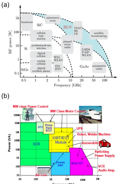
MtM trend is much more important for several applications employed active devices, such as analog/RF, e.g., wireless communication, and HV power, e.g. power switching, which are required to operate at high speed and high power. High-speed operation increases the communication rate, which is effective usage of frequency resources. In addition, high-power operation enhances long-range communication, high-efficiency, and miniaturization of the systems [5]. Therefore, to enhance the performance of the wireless communication systems, high-speed and high-power semiconductor active devices are important. Figure 1.3(a) exhibits a relation of RF power and frequency (speed) for several wireless-communication applications [6]. Similarly, the requirements are also hold for HV power applications. Fig. 1.3(b) shows relation of RF power and frequency for several power-switching applications [7]. From these figures, we can see that the devices which are required to operate at high speed can not transfer high power. On the other hand, the devices which are required to transfer high power can not operate at high speed. Although there is a trade-off between speed (frequency) and power for both applications, wide-gap semiconductor devices, such as GaN-based devices, have potentials to overcome the trade-off.
We discuss in details the trade-off between speed and power from material points of view.
For high speed, high electron mobility and saturation velocity are preferred, in which electron mobilityµis given by
µ= eτ m∗, and saturation velocityvsat is given by
vsat∼
√~ωop m∗ ,
with electron chargee, relaxation timeτ, optical phonon energy ~ωop, and electron effective mass m∗ [8]. In this sense, small m∗ is advantageous. On the other hand, for high power,
Figure 1.3: Relation of RF power and frequency for (a) several wireless-communication ap- plications [J.-Y. Duboz], and (b) several power-switching applications [H. Wang]. There is a trade-off between power and speed (frequency) for both device applications.
i.e., high voltage, high breakdown fieldFbr is desired, in which Fbr∝Egα,
with energy gapEg andα≃1-3 [5, 9]. This indicates that wideEgis advantageous. However, a trend of proportional relationm∗ ∝Eg, as shown in Fig. 1.4, exists in general cases. This leads to the trade-off between speed and power. Fortunately, wide-gap semiconductor GaN has possibilities to overcome the trade-off.
0.00 0.05 0.10 0.15 0.20 0.25
0.0 0.5 1.0 1.5 2.0 2.5 3.0 3.5 4.0 m*/m0
Eg [eV]
GaN
GaAs InAs GaSb
InSb
m*∝ Eg
InGaAs InGaSb
Figure 1.4: Electron effective massm∗ at Γ point as a function of energy gapEg for several III-V compound semiconductors.
1.2 GaN-based materials and devices
1.2.1 Advantageous properties of GaN-based materials
Wide-gap compound semiconductor GaN
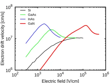
Figure 1.5 shows relation between lattice constant in a-axis and energy gap Eg and cor- responding emission wavelength for several wurtzite-nitride materials [10], in which GaN exhibits a wideEg of 3.39 eV [11]. This leads to a highFbr∼3.3 MV/cm, an advantageous for high power, but also a large m∗, shown in Fig. 1.4. This is disadvantageous. However, GaN has a large optical-phonon energy ~ωop ≃ 90 meV [12] and a large valley-separation energy, as depicted in Fig. 1.6 [13]. From this, we carried out Monte-Carlo simulation and obtained electron transport in GaN, depicted in Fig. 1.7, in which GaN shows not very high electron mobility, but high peak and saturation velocity, which are advantageous for high speed. Therefore, GaN is anticipated to overcome the trade-off between speed and power in semiconductor devices.
Figure 1.5: Relation between energy gap and lattice constant in a-axis for several wurtzite- nitride materials [I. Vurgaftmanet al.].
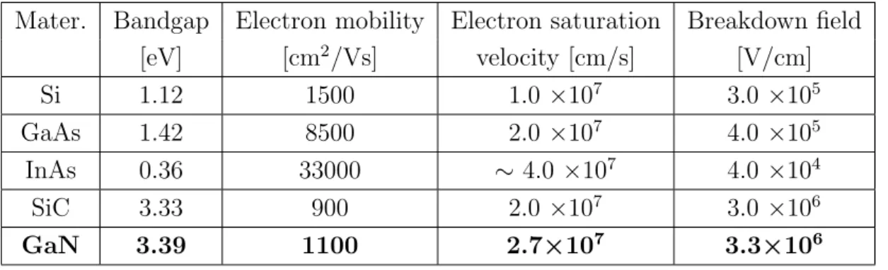
Table 1.2: Advantageous properties of GaN in comparison with other semiconductors.
Mater. Bandgap Electron mobility Electron saturation Breakdown field [eV] [cm2/Vs] velocity [cm/s] [V/cm]
Si 1.12 1500 1.0 ×10⁷ 3.0 ×10⁵
GaAs 1.42 8500 2.0 ×10⁷ 4.0 ×10⁵
InAs 0.36 33000 ∼ 4.0 ×10⁷ 4.0 ×10⁴
SiC 3.33 900 2.0 ×10⁷ 3.0 ×10⁶
GaN 3.39 1100 2.7×10⁷ 3.3×10⁶
Table 1.2 shows advantageous properties of GaN at 300 K in comparison with other
Figure 1.6: Energy band structure for wurtzite GaN [C. Bulutay et al.].
106 107 108
102 103 104 105 106
Electron drift velocity [cm/s]
Electric field [V/cm]
Si GaAs InAs GaN
Figure 1.7: Relation between electron drift velocity and electric field obtained by Monte Carlo simulation for several semiconductor materials.
semiconductors [5]. Using the table, we plotted Johnson figure of merit, given by fTVbr 6 Fbrvsat
2π , (1.1)
where fT is cut-off frequency and Vbr is breakdown voltage [14], showing products of the maximum cut-off frequencies and the maximum breakdown voltagesVbr, as depicted in Fig.
1.8. We also plotted Baliga figure of merit, given by Ron > 4Vbr2
ε0kµFbr3 (1.2)
or
Vbr2
Ron 6 ε0kµFbr3
4 , (1.3)
with vacuum dielectric constantε0 [15], showing relation between the maximum Vbr and the minimum on-resistances Ron, as depicted in Fig. 1.9. From these figures, we can see that GaN is more superior than other semiconductors.
Figure 1.8: Johnson figure of merit showing relation between maximum breakdown voltage Vbr and maximum cut-off frequency fT for several semiconductors [E. O. Johnsonet al.].
Figure 1.9: Baliga figure of merit showing relation between minimum on-resistanceRon and maximum breakdown voltageVbr for several semiconductors [B. J. Baliga].
Two-dimensional electron gas in AlGaN/GaN heterostructure
The formation of two dimensional electron gases (2DEG) in AlGaN/GaN heterostructures relies on both spontaneous and piezoelectric polarization induced effects [16, 17]. The spon- taneous polarization is due to an intrinsic asymmetry of the bonding in equilibrium wurtzite crystal structures of AlN and GaN. Piezoelectric polarization comes from mechanical stress, or tensile (compressive) strain of AlGaN and GaN layers. The details of these mechanisms are discussed as follows.
Figure 1.10: Wurtzite crystal structure of GaN with Ga-face. The growth direction is [0001].
Figure 1.10 shows a wurtzite crystal structure of GaN (or AlN), in which a0 is the edge length of the basal hexagon,c0 the height of the hexagonal prism at equilibrium. Structure parameters of the GaN and AlN are listed in the table 1.3 [17], in which, the parameteru is defined as the ratio of bonding lengthb0 and the heightc0 at equilibrium.
In the absence of external electric field and strain, the polarization inside the material is spontaneous. We consider the polarization along the [0001] direction (z-direction), since this
Table 1.3: Lattice constants a0, c0, c0/a0, bonding length b0, and parameter u = b0/c0 at equilibrium of GaN and AlN.
a0 [˚A] c0 [˚A] c0/a0 b0 [˚A] u=b0/c0 AlN 3.11 4.98 1.60 1.91 0.380 GaN 3.19 5.19 1.63 1.95 0.376
is the direction using for film growth. The spontaneous polarization along the direction is
Psp=Pspˆz. (1.4)
Because of the sensitive dependence of the spontaneous polarization on the structure pa- rameters, there are some quantitative differences in the polarization for GaN and AlN. The electronegativity number of Al∼1.6 and Ga∼1.8 are smaller than that of N∼3.0, which create a dipole, i.e., polarization, in Ga-N and Al-N bonds, whose direction is from N to Ga or Al. Table 1.4 shows the spontaneous polarization of GaN and AlN, which are negative. [16].
This indicates that for Ga(Al)-face heterostructures the spontaneous polarization is pointing towards the substrate as shown in Fig. 1.11.
Figure 1.11: Two-dimensional electron gas (2DEG) with high sheet carrier concentration formed by spontaneous and piezoelectric polarizations at the AlGaN/GaN (InAlN/GaN) heterointerface
Piezoelectric or strain-induced polarization Ppe is defined from piezoelectric coefficient tensoreil and strain tensorεhk [16]
Ppe=eilεhk. (1.5)
For wurtzite structure, the piezoelectric coefficient tensoreil has form
eil=
0 0 0 0 e15 0
0 0 0 e15 0 0
e31 e31 e33 0 0 0
, (1.6)
and the strain tensorεhk has form
εhk=
εxx
εyy εzz εyz εzx
εxy
, (1.7)
in whichεxx, εyy, εzz are stress strains andεyz, εzx, εxyare shear strains. In the case of without external force, stress strain is dominant. Therefore,Ppe can be calculated as
Ppe=e31(εxx+εyy) +e33εzz, (1.8) where εzz = (c−c0)/c0 is the strain along the z-axis and εxx =εyy = (a−a0)/a0 are the in-plane strain, in whicha0 and c0 are the equilibrium values of the lattice parameters. In the case of no force acting on z-axis, we have the relation
C33ezz =−2C13exx, (1.9)
where C33 and C13 are elastic constants. Using Eq. (1.8) and (1.9), the amount of the piezoelectric polarization in the direction of the z-axis can be determined by
Ppe=−2εxx(e31−e33
C13
C33
) or
Ppe=−2(a−a0) a0
(e31−e33
C13
C33
). (1.10)
Table 1.4: Calculated the spontaneous polarization and piezoelectric constants of AlN and GaN wurtzites.
Psp [C/m2] e33 [C/m2] e31 [C/m2]
AlN -0.081 1.46 -0.60
GaN -0.29 0.73 -0.49
Table 1.4 shows calculated values of e33 and e31 [16]. From eq. (1.10), we can say that Ppe is negative for tensile and positive for compressive strain. For AlGaN growth on GaN, the strain is tensile, depicted in Fig. 1.11, indicating thatPpe is in the same direction with Psp.
The gradient of polarization of in space generates induced charges. At an abrupt interface of AlGaN/GaN heterostructure the polarization can decrease or increase, causing a polariza- tion sheet charge density. For AlGaN growth on GaN with Ga-face, the total polarizationP, the sum of the spontaneous polarizationPsp and the piezoelectric polarization Ppe, is neg- ative, which induces electrons accumulating near the AlGaN/GaN interface. Owing to the strongP, the density of the accumulating electrons is large, which form a two-dimensional electron gas (2DEG) near the interface of the AlGaN/GaN heterostructures. Figure 1.12
shows calculated sheet charge density caused by spontaneous and piezoelectric polarization at the lower interface of a Ga-face GaN/AlGaN/GaN heterostructure v.s. alloy composition of the barrier, obtained by O. Ambacheret al.[18], indicating the high electron density of the 2DEG. As a result, the 2DEG can be utilized as the channel for GaN-based heterojunction field-effect transistors (HFETs). [19].
Figure 1.12: Calculated sheet charge density caused by spontaneous and piezoelectric po- larization at the lower interface of a Ga-face GaN/AlGaN/GaN heterostructure v.s. alloy composition of the barrier [O. Ambacheret al.].
1.2.2 GaN-based Schottky-HFETs and MIS-HFETs
Using the 2DEG as a channel, GaN-based Schottky-HFETs have been intensively investigated for high-speed, high-power, and high-temperature device applications [19–24]. High drain current, high transconductance, especially high cut-off frequencyfT and maximum frequency fmax were obtained. For example, G. J. Sullivan et al. fabricated a AlGaN/GaN Schottky- HFET with a gate length of 0.7µm on SiC substrate which showed a high current of∼1100 mA/mm, a transconductance of ∼ 270 mS/mm, fT ∼ 15 GHz and fmax ∼ 42 GHz [23].
However, AlGaN/GaN Schottky-HFETs exhibit high gate leakage current in spite of large energy gap [21, 25–27] and serious current collapse due to due to surface electron trapping [28–30], as depicted in Fig. 1.13(a). As a result, the reliability and life time of the devices are reduced.
Figure 1.13: Schematic cross section of GaN-based (a) Schottky-HFETs and (b) Metal- insulator-semiconductor (MIS)-HFETs.
In order to solve the problems, GaN-based metal-insulator-semiconductor (MIS)-HFETs, where a gate insulator is inserted between the metal and semiconductor, as depicted in Fig.
1.13(b), have been investigated owing to the merits of gate leakage reduction [27, 31–37]
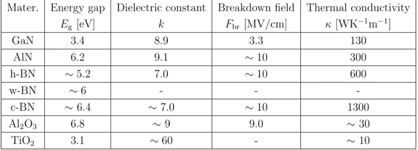
and passivation to suppress the current collapse [28–30], as shown in Fig. 1.13(b). Gate insulators, such as Al2O3 (Eg ∼ 6.8 eV, k ∼ 9 [38]) [34, 35, 39–42], HfO2 (Eg ∼ 5.8 eV, k ∼ 25 [43]) [32, 33, 44], TaON (Eg ∼ 4.3 eV, k ∼ 24) [37], and TiO2 (Eg ∼ 3.1 eV [45], k ∼ 60 [43]) [46–48]. and high-k nitrides, such as SiN (Eg ∼ 5.0 eV, k ∼ 7.5 [49]) [46, 47, 50, 51] and AlN (Eg ∼ 6.2 eV [52], k ∼ 9 [53]) [28–30, 36, 51, 54–56] have been intensively investigated. However, further developments of the MIS-HFETs using novel gate insulators suitable according to applications are important. A desired gate insulator should have:
• wide energy gap and high breakdown field Fbr for high voltage operation
• high dielectric constant kfor high transconductance
• high thermal conductivity κ for good heat release suitable to high power operation In particular, boron nitride (BN) and aluminum titanium oxide (AlTiO: an alloy of TiO2and Al2O3) are promising candidates.
1.3 BN and AlTiO as a high-dielectric-constant (high-k) insulator
1.3.1 Boron nitride (BN)
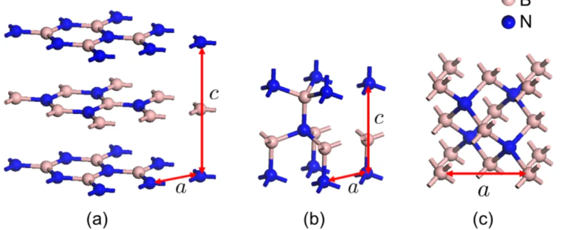
Boron nitride (BN) has been the subject of numerous theoretical and experimental studies.
It can occur in multiple polytypes, including white-graphite BN (h-BN), wurtzite BN (w- BN), and zincblende BN (c-BN) [57–63]. Similar to graphite, the h-BN has a white-graphite structure with sp2-hybridized B-N bonds [59, 64, 65] shown in Fig. 1.14(a). In contrast to graphite with C-C bondings showing strong covalent character, which exhibits semimetallic behavior, h-BN with B-N bonds showing ionic character, is insulating with an indirect energy gap Eg. It is in a range from 3.6 to 6.0 eV for theoretical calculations [57, 58, 60–63]
and ∼ 5 eV for experimental measurements [64, 66–70]. The wide Eg and the ability to synthesize single layers of the h phase make it attractive for two-dimensional electronics and as a substrate for growth or bonding of graphene [71]. In addition, the h-BN possesses a high thermal conductivityκ∼600 WK−1m−1 and high heat capacity [72].
Figure 1.14: Crystal structures of BN polymorphs: (a) zincblende, (b) wurtzite, and (c) white-graphite, obtained by Materials Studio.
On the other hand, the w-BN has a wurtzite structure with sp3-hybridized B-N bonds, as shown in Fig. 1.14(b), [59, 64]. Theoretical calculations show its indirectEg in a rang from 4.4 to 6.5 eV [57, 60–63]. The w-BN is metastable at all temperatures, and a large volume expansion occurs on conversion of the wurtzitic form to the other forms [73]. Therefore,Eg
of w-BN is difficult to be determined by experimental methods.
In contrast, the c-BN, which is stable and ultra-hard, has a zincblende structure with sp3- hybridized B-N bonds [59, 64, 65, 74], as shown in Fig. 1.14(c). The c-BN has an indirect Eg, which is in a range from 4.2 to 7.2 eV for theoretical calculations [57, 58, 60–63] and
∼ 6.4 eV for experimental measurements [75]. The wide Eg of the c-BN leads to its high breakdown field∼10 MV/cm [52]. In addition, the c-BN has a high melting point∼3000◦C [76], high dielectric constantk∼7 [77], and very high κ∼1300 WK−1m−1 [78, 79]. This is
∼4 and∼40 times higher than that of AlN and Al2O3, respectively. Table 1.5 lists physical
properties of BN polymorphs in comparison with other insulators. Figure 1.15 draws band lineup of BN polymorphs and several insulators in an alignment with AlGaN and GaN. We observe a wide conduction-band difference between BN polymorphs and AlGaN.
Table 1.5: Advantageous properties of BN polymorphs in comparison with other materials.
Mater. Energy gap Dielectric constant Breakdown field Thermal conductivity Eg [eV] k Fbr [MV/cm] κ[WK−1m−1]
GaN 3.4 8.9 3.3 130
AlN 6.2 9.1 ∼10 300
h-BN ∼5.2 7.0 ∼10 600
w-BN ∼6 - - -
c-BN ∼6.4 ∼7.0 ∼10 1300
Al2O3 6.8 ∼9 9.0 ∼ 30
TiO2 3.1 ∼60 - ∼ 10
Figure 1.15: Band lineup for BN polymorphs and several insulators, in comparison with AlGaN/GaN.
Owing to the advantageous properties of BN polymorphs, they can be favorable gate insulators [80, 81]. There was a report on BN gate insulator for GaN-based devices by J.-C.
Gerbedoenet al.[82], in which h-BN films were obtained by chemical vapor deposition. How- ever, device performance was poor, such as a low maximum drain current ∼ 590 mA/mm, and a low extrinsic transconductance ∼ 60 mS/mm. In addition, electron transport prop- erties for channel conduction and gate leakage were not clarified. Therefore, it is worth to study BN and its applications to BN/AlGaN/GaN MIS-HFETs in details. In this thesis, we will characterize physical properties of BN thin films obtained by RF magnetron sput- tering. Using such films, we will fabricate BN/AlGaN/GaN MIS-HFETs, and investigate their temperature-dependent characteristics. We will analyze electron transport properties for channel conduction and gate leakage, and from the latter we will estimate BN/AlGaN interface state density.
1.3.2 Aluminum titanium oxide (AlTiO)
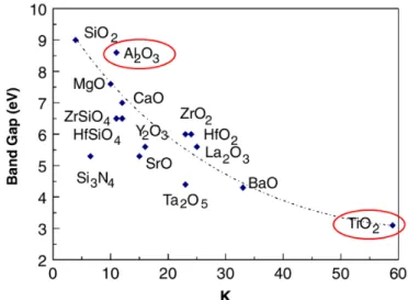
Figure 1.16: Relation between dielectric constantkand energy gap Eg for several oxides [J.
Robertson].
Figure 1.16 depicts relation between dielectric constant k and energy gap Eg for several oxides [43]. There is a trade-off between highk and high Eg. Owing to an extremely high kof TiO2 (∼60), TiO2/AlGaN/GaN MIS-HFETs were investigated [46, 48]. Unfortunately, the small energy gapEg of TiO2 (∼3.1 eV) [45] is a drawback, leading to high gate leakage currents [46, 48] and low breakdown fields [83]. On the other hand, Al2O3 has a wideEg∼6.8 eV, which exhibits very good insulating properties [34, 40, 42]. However, it shows a lower k ∼ 9 [38]. In order to realize not only high k but also wide Eg, a combination of TiO2 and Al2O3 may be possible. AlTiO, an alloy of TiO2 and Al2O3, which has intermediate properties between TiO2 and Al2O3, as shown in Fig. 1.17, is important to balance k and Eg.
Figure 1.17: AlTiO, an alloy of TiO2 and Al2O3, has intermediate properties between TiO2
and Al2O3.
There were some reports on AlTiO gate insulator for Si-based devices [84–86] and GaAs- based devices [87–89]. However, there was no report on AlTiO gate insulator for GaN-based devices. In order to obtain AlTiO films, several deposition methods, such as sputtering de- position [84], pulsed laser deposition [85], and atomic layer deposition (ALD) [86–89], were utilized. In particular, the ALD is advantageous to produce high-quality films with high reproducibility and fine composition control. In this thesis, we will characterize physical properties of AlTiO thin films obtained by atomic layer deposition, for several Al composi- tions. Using such films, we will fabricate AlTiO/AlGaN/GaN MIS-HFETs, and investigate their temperature-dependent characteristics. In addition, we will analyze electron transport properties for channel conduction and gate leakage, and from the latter we will estimate AlTiO/AlGaN interface state density.
1.4 Purposes of this study
In order to develop the AlGaN/GaN MIS-HFETs using novel gate insulators suitable for high-speed and high-power applications, we study BN and AlTiO high-kgate insulators.
At first, in order to check BN films obtained by RF magnetron sputtering deposition, BN/n-Si(001) will be characterized by ellipsometry and MIS-capacitor I-V measurements.
We will optimize BN deposition conditions, for example N2ratio, to obtain highest BN quality.
Then, BN will be deposited on an AlGaN/GaN heterostructure, which will be characterized by X-ray diffraction (XRD) and X-ray photoelectron spectroscopy (XPS). Using the BN films, we will fabricate BN/AlGaN/GaN MIS-HFETs and investigate their gate leakage and ambient-dependent characteristics. We will also investigate their temperature-dependent characteristics; analyze electron transport properties for channel conduction and gate leakage, and estimate BN/AlGaN interface state density.
Similarly, in order to check AlTiO films obtained by ALD, AlTiO/n-GaAs(001) will be characterized by ellipsometry, XPS, and MIS-capacitor I-V measurements. We will charac- terize physical properties of AlTiO thin films, for several Al compositions. Using a trade-off composition, AlTiO will be deposited on the same AlGaN/GaN heterostructure, which will be characterized by XRD. Using the AlTiO films, we will fabricate AlTiO/AlGaN/GaN MIS-HFETs and investigate their gate leakage and compare with Al2O3/AlGaN/GaN MIS- HFETs. For the AlTiO/AlGaN/GaN MIS-HFETs, we will also investigate their temperature- dependent device characteristics; analyze electron transport properties for channel conduction and gate leakage, and estimate AlTiO/AlGaN interface state density. Finally, we will briefly compare BN and AlTiO as high-k gate insulators.
1.5 Organization of the dissertation
We organize this dissertation into 5 chapters. In chapter 1, at the beginning, we introduce trends of recent semiconductor industry: More Moore and More than Moore. The trade- off between speed and power in semiconductor devices, advantages of GaN to overcome the trade-off are mentioned. We explain the formation of two dimension electron gas at AlGaN/GaN interface. Then, we briefly review researches on GaN-based devices with several oxide and nitride high-kinsulators. In details, we evaluate researches on BN and AlTiO, their advantageous properties and applications to AlGaN/GaN HFETs and MIS-HFETs.
Next, in chapter 2, we briefly describe general fabrication process methods for AlGaN/GaN MIS-HFETs. We explain some key points during the process flows, and summary in details conditions for each step.
Then, in chapter 3, we describe a RF magnetron sputtering deposition method to obtain BN films. Fabrication process and I-V characteristics of BN/n-Si(001) MIS capacitors are shown in this chapter. We show XRD and XPS measurement results of BN films on Al- GaN/GaN/sapphire(0001). Using the films, we fabricate BN/AlGaN/GaN MIS-HFETs and investigate their characteristics in different ambiences and their temperature dependence of output and transfer characteristics. This chapter shows analysis results of electron transport properties for channel conduction and gate leakage, and estimation of BN/AlGaN interface state density.
After that, in chapter 4 we describe ALD method to obtain AlTiO films. We show rela- tion between Al composition and AlTiO film properties, such as refractive index, energy gap, breakdown field and dielectric constant. We apply a trade-off composition for AlTiO deposi- tion to fabricate AlTiO/AlGaN/GaN MIS-HFETs and show their gate leakage and compari- son with Al2O3/AlGaN/GaN MIS-HFETs. This chapter also shows temperature dependence of output and transfer characteristics for AlTiO/AlGaN/GaN MIS-HFETs, analysis results of electron transport properties for channel conduction and gate leakage, and estimation of AlTiO/AlGaN interface state density.
Finally, we conclude this work, briefly compare BN and AlTiO Future works are also mentioned.
Fabrication process methods for AlGaN/GaN MIS-HFETs
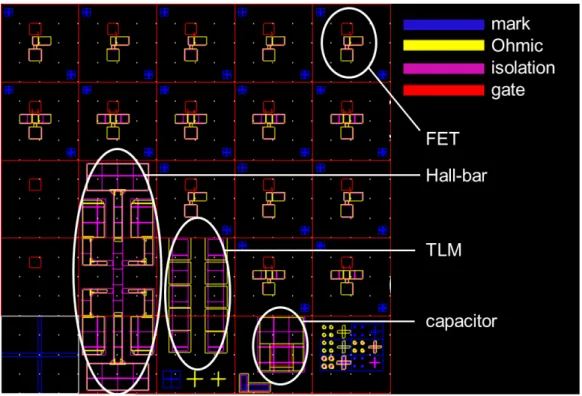
Mask pattern using for device fabrication in this research is shown in Fig. 2.1. For evaluat- ing electrical characteristics during the fabrication process, FET, Hall-bar, transmission line model (TLM), and capacitor are fabricated simultaneously. The fabrication process methods for AlGaN/GaN MIS-HFETs includes five steps as follows.
1. Marker formation
2. Ohmic electrode formation 3. Device isolation
4. Gate insulator deposition 5. Gate electrode formation
We describes in details of all steps as follows.
2.1 Marker formation
Marker formation is an important step because markers were utilized to align for all follow- ing steps: Ohmic electrode formation, device isolation, and gate electrode formation. For this device fabrication process, we employed an AlGaN/GaN heterostructure, obtained by Metal-Organic Vapor Phase Epitaxy (MOVPE ) grown on sapphire(0001) substrate. Marker formation was started by a surface treatment for the heterostructure using organic solvents and O2 plasma ashing for removing organic contaminants, followed by ammonium-based so- lutions (Semico-clean) for removing oxides. A clean surface can enhance adhesion between metals and the AlGaN surface. Then, a metal structure of Titanium/Gold (Ti/Au) = 10/150 nm was deposited on the heterostructure by an e-beam evaporator. Conditions of steps and processing for marker formation are listed in Tab. 2.1.
20
Figure 2.1: Mask pattern with test element groups: FETs, Hall-bars, transmission line models (TLM), and capacitors. Grid size is 125µm.
Table 2.1: Marker formation process flow.
Process Conditions
surface treatment - acetone, methanol, DIW 3 min each - O2 plasma ashing 50 Pa 10 W 4 min - Semico-clean 5 min, DIW 3 min - bake 110◦C 3 min
resist coating - LOL2000 3000 rpm 60 s, bake 180◦C 180 s - TSMR-8900 4000 rpm 60 s, bake 110 ◦C 90 s patterning - exposure ∼12 mW/cm2 (405 nm) 6.2 s
- development NMD-W 60 s, DIW 180 s surface treatment - O2 plasma ashing 50 Pa 10 W 10 s
- Semico-clean 5 min, DIW 3 min deposition - Ti/Au = 10/150 nm
lift-off - 1165 60 ◦C∼ 30 min
- acetone, methanol, DIW 3 min each
2.2 Ohmic electrode formation
Conditions of steps and processing for Ohmic electrode formation are listed in Tab. 2.2 and shown in Fig. 2.2.
Table 2.2: Ohmic electrode formation process flow.
Process Conditions
surface treatment - acetone, methanol, DIW 3 min each - O2 plasma ashing 50 Pa 10 W 4 min - Semico-clean 5 min, DIW 3 min - bake 110◦C 3 min
resist coating - LOL2000 3000 rpm 60 s, bake 180◦C 180 s - TSMR-8900 4000 rpm 60 s, bake 110 ◦C 90 s patterning - exposure ∼12 mW/cm2 (405 nm) 6.2 s
- development NMD-W 60 s, DIW 180 s surface treatment - O2 plasma ashing 50 Pa 10 W 10 s
- Semico-clean 5 min, DIW 3 min deposition - Ti/Al/Ti/Au = 10/200/100/50 nm lift-off - 1165 60 ◦C∼ 30 min
- acetone, methanol, DIW 3 min each annealing - N2 ambience
Low contact resistance and high stability are important requirements for FET electrodes.
In our device fabrication process, an electrode structure of Titanium/Aluminium/Titanium/Gold (Ti/Al/Ti/Au) = 10/200/100/50 nm was deposited on the AlGaN/GaN heterostructure by the e-beam evaporator. Ti with a low work function∼4.3 eV [90], exhibits very low barrier height to n-GaN [91]. However, the main reason of using Ti is its ability to extract N out of the AlGaN(GaN) by formation of TiN due to reaction between Ti and N,
2Ti + N2 = 2TiN,
during annealing process. This leaves a high density of N vacancies below the electrodes, acting as donor dope and giving electrons [92]. High electron densities can create tunnel junctions, or Ohmic contacts [93]. Al in the metalization scheme forms an alloy with the Ti layer below, by which the aggressive Ti-GaN reaction is decreased and maintain the TiN layer [94]. Au is deposited as the final metal layer to exclude oxidation of the contact. Ti layer beneath Au has a role to limit the diffusion of Au into the layers below and vice versa.
From transmission line model (TLM) measurements, contact resistance Rc of the Ohmic contacts and sheet resistanceρs were obtained by a linear fitting for measurement resistance R to electrode spacingL using
R(L) = 2Rc+ρsL. (2.1)
Figure 2.2: Ohmic electrode formation process flow.
![Figure 1.2: The dual trend in the International Technology Roadmap for Semiconductors (ITRS): miniaturization of the digital functions (“More Moore”) and functional diversification (“More-than-Moore”) [ITRS 2011].](https://thumb-ap.123doks.com/thumbv2/123deta/6077608.1073831/19.892.246.678.714.1000/international-technology-roadmap-semiconductors-miniaturization-functions-functional-diversification.webp)