INVITED PAPER
Special Section on Photonic Devices using Nanofabrication Technology and Their ApplicationsPhotonic Crystal Nanolaser Biosensors
Shota KITA†,††a), Shota OTSUKA†,††, Shoji HACHUDA†,††, Tatsuro ENDO†††, Yasunori IMAI†††, Yoshiaki NISHIJIMA††††, Hiroaki MISAWA††††,Nonmembers,andToshihiko BABA†,††,Member
SUMMARY High-performance and low-cost sensors are critical de- vices for high-throughput analyses of bio-samples in medical diagnoses and life sciences. In this paper, we demonstrate photonic crystal nanolaser sensor, which detects the adsorption of biomolecules from the lasing wave- length shift. It is a promising device, which balances a high sensitivity, high resolution, small size, easy integration, simple setup and low cost. In particular with a nanoslot structure, it achieves a super-sensitivity in pro- tein sensing whose detection limit is three orders of magnitude lower than that of standard surface-plasmon-resonance sensors. Our investigations in- dicate that the nanoslot acts as a protein condenser powered by the optical gradient force, which arises from the strong localization of laser mode in the nanoslot.
key words: photonic crystal, nanolaser, nanoslot, liquid sensor, biosensor
1. Introduction
Protein analyses are increasing demands for medical diag- nosis, health care, food evaluation, proteomics, and so on.
In particular, high-throughput and low-cost assay of a target protein in a small amount of analyte is desired and stud- ied [1]. Lab-on-a-chip and micro-total analysis systems (μ- TAS) [2] have been developed as supplementary tools that control fluids and promote the reactions in the target. Simi- larly, developing novel principles and methods in sensors is becoming an important issue [3]. At present, labeling meth- ods are commonly used for sensing. Here, fluorescent mol- ecules are functionalized as labels to the target so that the behaviors of the target is observed directly through versatile instruments such as fluorescent optical microscopes. How- ever, the complicated functionalization process is a bottle- neck for high throughput and cost reduction. In addition, the functionalization itself remains an uncertainty if it maintains the original behaviors of the target.
As alternatives, various label-free methods have been studied and developed. Fundamentally, they are required to satisfy the following requirements:
1) High performance: The most fundamental spec of bio- Manuscript received July 1, 2011.
Manuscript revised November 1, 2011.
†The authors are with Yokohama National University, Yokohama-shi, 240-8501 Japan.
††The authors are with CREST, Japan Science and Technology Agency, Tokyo, 105-0075 Japan.
†††The authors are with Tokyo Institute of Technology, Yokohama-shi, 226-8502 Japan.
††††The authors are with Hokkaido University, Sapporo-shi, 001- 0021 Japan.
a) E-mail: [email protected] DOI: 10.1587/transele.E95.C.188
sensors is the detection limit (DL) meaning the minimum detectable concentration of the target in the analyte. It is determined by the sensitivity of the sensor and also by the resolution of the sensor and other equipments, which is affected by noise. For high-throughput assay simply checking the presence of the target without pre- concentration process, a low DL of the order of or even lower than 1 pM is necessary [1] (DL of labeling meth- ods is usually of nM order and sometimes reaches to pM order in researches). The quantization of the target is sometimes required in medical applications, and a wide dynamic range showing a linear response is necessary for this. Of course, the stability of results and insensi- tivity to the measurement condition reduce the noise and improve the reliability and usability.
2) Low cost: To avoid the mutual contamination of sam- ples, the disposable use of sensors is preferable, and therefore, the sensor cost is crucial. In addition, hours of work for sensing also reflect to the total analysis cost.
Regarding this point, neglecting the functionalization of labels is already advantageous. A low DL allowing skip- ping the pre-concentration process adds another advan- tage.
3) Functionality: If we can monitor the realtime response of the sensing, it is useful for analyzing the kinetics of reaction. If the multi-information can be obtained simul- taneously for multi-targets, it enhances the throughput and enables statistical analyses.
4) Usability: A simple and portable system is desirable so that anyone can use anywhere. For this purpose, down- sizing the total system is necessary, and this also con- tributes to the integrability. The disposable use is also important for this.
5) Integrability: If sensors are integrated withμ-TAS, it will be a powerful inspection kit that achieves high perfor- mance in terms of throughput, stability and functionality.
For this purpose, sensors must have a size comparable to or even smaller than fluidic channels in μ-TAS, which usually have a feature size of 10μm order.
Table 1 summarizes the performance and other fea- tures of label-free biosensors reported so far. Fundamen- tally, all of them use the same procedure of the sensing.
First, a host material known to bind specifically with the tar- get guest protein is functionalized onto the sensor surface.
Then, the sample containing the target is injected and the Copyright c2012 The Institute of Electronics, Information and Communication Engineers
Table 1 Comparison of label-free biosensors.
specific binding is detected by the sensor. Such two step process is much simpler than labeling methods including additional functionalization of labels. The most common sensor is the surface plasmon resonance (SPR) sensor [4].
It measures the resonant angle of incident light coupled to the surface plasmon mode of a metal, and detects its shift against the presence of the target on the metal. The system is easy to use but hard to miniaturize, and its DL is on an average level due to the broad resonant spectrum, which de- grades the resolution. The local plasmon resonance at metal nanoparticles [5] and surface-enhanced Raman scattering at rough metal surfaces [6] achieve an ultralow DL through the highly sensitive spectral shift, but the signal is noisy and un- stable. Field effect transistors (FETs) modified by carbon nanotubes (CNT) [7], [8] or graphene [9] can detect the spe- cific binding through the change of the electric characteris- tics. Such one chip device is easy to handle, but may be too expensive for disposable use. In addition, they do not show a good DL and robust signal simultaneously.
Optical micro/nanocavities are also exploited as sen- sors [10]. Here, tunable laser light is coupled to the device, the resonant spectrum is measured, and the binding is de- tected through the spectral shift. Cavities are categorized into the whispering gallery mode type (sphere [11], toroid
[12], ring [13], [14]) and the Bragg reflection type (grating [15], photonic crystal (PC) [16], [25]). Microspheres and microtoroids recorded an excellent DL thanks to ultranar- row spectral linewidths of less than 1 pm. However, such a narrow spectrum requires complicated measurement tools and leads to unwanted response against environmental fluc- tuations. Low cost manufacturing of microring and PC cav- ities will be possible by exploiting the CMOS-compatible technology in Si photonics [17], but their DL is not so good because of the relatively broad spectrum and moderate sen- sitivity. In addition, all of these passive cavities need the optical fiber coupling at input and output (I/O), which be- comes a barrier for cost reduction and disposable use.
In this paper, we focus on an alternative method us- ing lasers (in other words, active cavities). The fundamental principle is similar to that of passive cavities; the binding is detected through the lasing spectral shift. Standard stripe lasers and vertical cavity surface emitting lasers may also be applicable [18], but a high sensitivity is not expected as their laser mode is almost confined inside the semiconduc- tors. On the other hand, micro/nanolasers have laser modes whose large fraction of fields is penetrating to air, resulting in a high sensitivity [19]. In addition, they have the follow- ing advantages in comparison with passive cavities:
1) A high resolution is ensured by a narrow spectrum above the laser threshold. This eliminates a general constraint in passive cavities that a smaller cavity degrades itsQ and expands the spectrum. Thus, nanolasers can be downsized independently of the passive Q below the threshold if Q is sufficient for lasing. The lasing also eliminates the instability of passiveQeasily affected by the disordering.
2) Optical I/O are much more simplified than the case of passive cavities, since both the photopumping and the detection of laser emission can be done through free- space optics. Therefore, the sensor chip can be isolated from other measurement equipments. The chip cost will be almost negligible even though it is fabricated by using e-beam lithography, because the lithographic area is only (∼10μm)2for each chip. This allows the manufacturing of low cost disposable chips using a standard semicon- ductor process. Assuming two state-of-the-arte-beam writers, the throughput can be>14,000 chip/day. The chip cost can be much less than Y=100, even including costs for other facilities, materials, packaging, testing, staffs and yield.
3) The spectral shift for nanolasers is measured by a spec- trometer such as optical spectrum analyzer (OSA). Here, a high-speed spectral analysis is possible by using sen- sor arrays and mixing coarse and fine observations with changing the span and resolution. Such high-speed flex- ible measurement is not easy for passive cavities when a highQmode is searched by scanning the tunable laser source; the rough scanning can skip the cavity mode.
The performance of nanolaser in this work, i.e.
nanoslot (NS) photonic crystal (PC) H0-type nanolaser [20], [21], is compared with other biosensors in Table 1.
Since target proteins are different between reports, the affin- ity constantKA changes from 105 −1011M−1. In general, DL is improved by a largeKA. Therefore, the performance should be evaluated by the product of DL andKA. Let us define the figure-of-merit (FOM) factor as (DL×KA)−1nor- malized by that for the SPR sensor reported recently [22].
Then our nanolaser achieves a very high FOM of 230 − 2,300 assuming the intensity noise factorξ, which will be discussed in Sect. 3, to be 1.0−0.1, respectively.
To date, FOMs higher than these value have only been reported for Au nanoparticles [6] and micro-toroidal cavity [12], which have aforementioned drawbacks. This nanolaser is very unique because a large fraction of laser mode is strongly localized in the NS outside of semicon- ductors. This paper reports in detail later that this localiza- tion improves the thermal characteristics and resolution, and greatly enhances the sensitivity for biomolecules, resulting in the very low DL and high FOM. In Sect. 2, we first de- scribe the structure and laser characteristics of this device.
We particularly focus on effects of the NS for the thermal characteristics and resolution. In Sect. 3, we present the the- oretical sensing characteristics and experimentally demon- strate the sensing of liquids. In Sect. 4, we show biosensing
experiments for nonspecific and specific bindings, includ- ing realtime responses. We discuss the mechanism of the super-sensitivity arising from the NS.
2. NS PC Nanolaser
The PC H0 nanolaser without NS consists of the shift of nearest two or four airholes in a triangular lattice PC slab. The three-dimensional finite-difference time-domain (FDTD) simulation predicts that a device fabricated into GaInAsP quantum-well wafer with a lattice constant a = 500 nm, airhole diameter 2r = 260 nm, sx = 120 nm, sy = 80 nm, and slab thickness t = 200 nm has a pas- sive Q ∼ 100,000 and a modal volumeVm ∼ 0.15(λ/n)3, where λ is the wavelength and n is the material index at the mode maximum. We have already reported its room- temperature continuous-wave (cw) operation with a sub- μW threshold [21], [26], high-resolution liquid index sens- ing (∼9.0×10⁻⁵RIU) [21], [27] and protein sensing [28].
However, a broad spectral linewidth caused by the large thermal chirping [29] have degraded the sensing resolution [30]. To solve this problem, we incorporated the NS, which maintains the localized mode, as shown in Fig. 1. Similar mode has first been discussed in Ref. [31], and it has been exploited for reducingVmin a passive cavity [32], capturing biomolecules such as DNAs [33] and enhancing the liquid index sensitivity [34]. For a high-index-contrast interface of the NS, Maxwell’s equations dictate that, in order to sat-
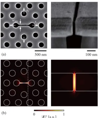
Fig. 1 NS nanolaser. (a) Scanning electron micrograph (SEM) of fabri- cated device. Details of fabrication are shown in Ref. [21]. (b) Calculated modal distribution for a nanoslot widthwNS=20 nm. Left and right panels depict in-plane and cross-sectional distribution, respectively. Dashed line shows the location of cross-section.
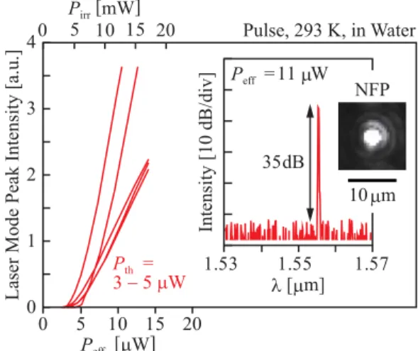
Fig. 2 Laser characteristics of NS nanolasers in water. Pirrshows irra- diation power of photopumping. Insets show near field pattern of lasing spectra and near field pattern.
isfy the continuity of the normal component of the electric flux densityD, the corresponding E field must undergo a large discontinuity with a much higher amplitude in the low- index side. This discontinuity strongly enhances the field and forms a localized mode in the low-index NS. In the case of NS nanolaser, it increases the total mode penetration out- side of semiconductors by 10–20%. Since the biosensing is usually performed in water-based analyte, the mode pene- tration enhances the sensitivity. Note that water has an ab- sorption coefficient of∼10 cm−1atλ∼1.55μm and a local maximum of∼30 cm−1at l.45μm [35]. It is a constraint in setting the modal wavelength, while a sufficiently highQof 10,000 is theoretically expected atλ ∼ 1.55μm even with the absorption, maintaining an extremely smallVm=0.006 (λ/nwater)3whensxandsyin Fig. 1(a) are optimized [21].
With sensor applications in mind, the laser character- istics were experimentally evaluated in water using pulsed photopumping at 980 nm (duty-ratio of 200, spot diameter of 20μm for efficient pumping of the NS mode [21]) and the laser emission was detected using a fluorescence micro- scope setup. The laser spectrum was analyzed by OSA with a resolution of 10 pm. Figure 2 shows the results for several devices with a NS widthwNS of 30–60 nm. Here, the effec- tive pump powerPeff was estimated by counting the spatial overlap of the pump spot with the effective modal area and its imperfect absorption in the slab [21]. Clear lasing is ob- served with a 35 dB peak intensity at an effective threshold of 3–5μW. Figure 3 compares the lasing spectra with and without the NS. As mentioned above, the spectrum without NS under pulsed condition widely broadens due to the ther- mal chirping. The full-width at half-maximum (FWHM) of the spectrum, Δλw, is over 600 pm in water, which is 15 times narrower than in air [29] but still broad. In contrast, it narrows drastically to 18 pm with the NS, which is close to the resolution limit of the OSA. Since water has a neg- ative thermo-optic coefficientΔn/ΔT ∼ −10−4RIU/K [36]
(RIU means the refractive index units), the positive coeffi- cient∼10−4RIU/K of GaInAsP slab can be canceled and the
Fig. 3 Comparison of pulsed lasing spectra in water between with and without NS.
Fig. 4 Comparison of wavelength shift due to (a) temperature and (b) irradiated power change between with and without NS.
thermal chirping can be suppressed by the appropriate mode penetration into the NS. This expectation was confirmed fur- ther by measuring the temperature dependence of the spec- tral shiftΔλswith and without the NS, as shown in Fig. 4(a).
Without NS, the shift increases almost linearly with temper- ature with a slope of 82 pm/K. With the NS, on the other hand, the dependence is reduced to four times smaller atT
=20◦C and almost eliminated (<3 pm/K) at 40◦C. This tem- perature dependence of athermalization can be explained by the quadratic thermo-optic coefficient of water [36]. Solid lines in Fig. 4 are obtained by taking account of these ef- fects with the modal profile in Fig. 1. They almost explain the experimental behaviors. This athermalization also re- flects to the power dependence of the spectral shift. It is reduced to six times smaller with the NS at T =20◦C, as shown in Fig. 4(b).
3. Sensing Characteristics
The nanolaser sensor detects the index change within the penetration depth of the laser mode (1/edepth is calculated to be 110–140 nm for the above devices) through the spec-
tral shift. The index resolutionΔnresis given by Δnres= Δλmin
Δλs
Δn −1
(1) whereΔλminis the minimum resoluble shift andΔλs/Δnis the sensitivity. Let us assume a Lorentzian spectrum I(λ) with the peak intensity Ipeak and peak wavelength λp, the wavelength shift amountΔλand the fluctuation noise in the wavelengthδλlimited by the stability of device and the ac- curacy of OSA, and intensity δI caused by the temporal change of pumping power and degradation of the device.
The intensity at the intersection point betweenλandλ+ Δλ is denoted asI(λp+ Δλ/2). The wavelength shiftΔλis de- tectable, whenIpeak−I(λp+ Δλ/2) is higher thanδI(Δλmin
is determined when they are equal). Solving this condition, addingδλand assumingIpeak> δI,Δλminis approximated as
Δλmin=ξΔλw+δλ, ξ=
1
Ipeak/δI−1 (2) ξ is the intensity noise factor showing how the intensity noise affects the wavelength fluctuation based on the as- sumedI(λ). In nanolasers under sensing,δI could be large because of the convection of water leading to the fluctua- tion in photopumping and light extraction condition. When Ipeak/δI=2, 5 and 10, the intensity noise factorξbecomes 1.0, 0.5 and 0.3, respectively. If data acquisition is suffi- ciently averaged by the statistic measurement,Ipeak/δI=100 andξ0.1 are obtainable. In the OSA used in this study, the wavelength reproducibility is<6 pm. The temperature fluctuation can be 0.5 K for long measurements, andδλbe- comes<15 pm and∼400 pm with and without NS, respec- tively. The noise induced from the pump source is smaller than this. Then, the sum of all the noise approximately gives Δλmin ∼ Δλw [21]. In realtime continuous measurements, short term fluctuations in temperature and OSA are suffi- ciently small. ThusδλΔλw, andΔλmin ∼ξΔλwwhereξ 0.1 is possible.
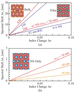
On the other hand, the sensitivity Δλs/Δn in the NS nanolaser is calculated by using the FDTD method, as shown in Fig. 5(a). Here, the uniform bulk medium (the index nb) simulates a liquid and the 20-nm-thick film (nf) on surfaces and sidewalls simulates the adsorption of biomolecules. The modal wavelength in water is used as a reference. The sensitivity for the filmΔλs/Δnf is 108 and 82 nm/RIU with and without the NS, respectively. Since the modal field overlaps with the film partially, the sensitivity is nearly four times smaller than that for bulk,Δλs/Δnb. The field component localized in the NS enhancesΔλs/Δnf by 25%. Figure 5(b) shows a similar calculation assuming the film only inside the NS. The spectral shift is smaller than (a), but a shift around 1 nm in this figure is still large enough to detect and resolve in our setup. The sensitivity is enhanced in inverse proportion towNS. While biosensing experiments are shown in the next section, Fig. 6 demonstrates the liq- uid index sensing. The sensitivity is obviously enhanced
Fig. 5 Spectral shift calculated with index change, where modal wave- length in water withnb =1.321 is used as a reference. (a) Comparison between bulk and film (20 nm thickness) index sensitivity. (b) Result for film only in NS.
Fig. 6 Spectral shift in different index liquids Cargille B0700/0701.
Spectral widths are different from those in Fig. 3 because of different pump- ing condition and different thermo-optic coefficients of index liquids.
from 280 nm/RIU without NS to 410 nm/RIU with the NS.
These values are in good agreement with the calculation in Fig. 5(a).
4. Biosensing
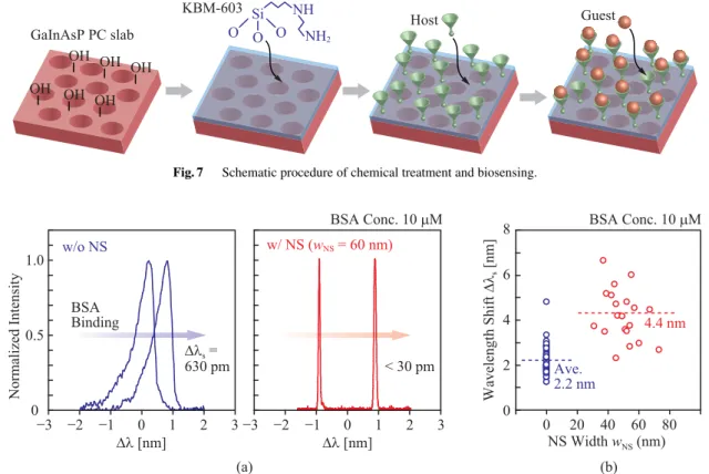
As mentioned earlier, label-free biosensing uses the two- step process, i.e. the host functionalization and guest ad- sorption. The fundamental procedure of this experiment including this process is depicted in Fig. 7. First, a hy- droxyl group is functionalized on the device surface with 9%
HCl/deionized water at 3◦C for more than 2 hours. Then,
Fig. 7 Schematic procedure of chemical treatment and biosensing.
Fig. 8 Sensing of BSA protein in the high concentration regime. (a) Wavelength shift before and after BSA adsorption. (b) Dependence of wavelength shift on NS width. Solid lines denote averages.
silanization is performed using 10% N-2-(aminoethyl)-3- aminopropyltrimethoxysilane (KBM-603, Shinetsu Chem- ical Co.) and a host material is subsequently functionalized at 20◦C for 1 hour. Finally, a target guest is adsorbed and the nanolaser detects it. After soaking the device in high- concentration (severalμM) guest aqueous solution for more than 30 minutes, we usually observe approximately 10-nm roughness on the device surface and in the NS using SEM, which is not observed before the process. This indicates the adsorption of the guest protein. In this experiment, we chose two combinations of host material and target guest material.
One combination is glutaraldehyde (GA) and bovine serum albumin (BSA, molecular weight=68 kDa) [37]. BSA is a common protein for test experiments in biosensing. It binds with GA nonspecifically with a relatively small affinity con- stant (∼107M−1order). The other combination is biotin and streptavidin (SA, molecular weight =53 kDa) [38]. This combination is often used as a model of host-guest specific binding. The affinity constant in this case is very large (>
1013M−1) [39].
Figure 8(a) shows laser spectra before and after the BSA adsorption when the BSA concentration was as high as 10μM. The spectrum clearly redshifted for both with and without the NS. Without the NS, the spectrum is broadened by the thermal chirping but the shift is still observed clearly.
With the NS, the spectrum is markedly narrowed and the resolution is drastically improved. Figure 8(b) summarizes the dependence of the redshift on the NS width. The average
shift with and without the NS are 4.4 nm and 2.2 nm, respec- tively. It means that a twice higher sensitivity was obtained by the NS. This enhancement is larger than that expected in the theoretical result of Fig. 5(a). This suggests that the NS not only improves the sensitivity but also accelerates the adsorption of BSA, which is further discussed below.
Figure 9(a) shows the spectral shifts for different BSA concentrations C. A large shift ShiftH is observed in the high-concentration regime of >10 nM for both with and without the NS. It is not saturated even at>100μM. This may be due to the physisorption, aggregation and phase tran- sition [40] of high-concentration BSA. On the other hand, a small shift ShiftLis observed clearly in the low concentra- tion regime only with the NS. This was observed repeatedly for all devices in different fabrication lots. Therefore, we can consider that ShiftLarises from the adsorption inside the NS, while ShiftHfrom the adsorption over all other surfaces.
Actually, we observed after the experiment that BSA is se- lectively adsorbed in/around the NS even atC =1 pM, as shown in the inset of Fig. 9(b). Usually, such dense adsorp- tion does not occur in a low concentration regime. Provided that each adsorption process occurs independently, Δλs is expressed as the sum of three different Langmuir adsorption isotherms [41]:
Δλs=Δλmax1KA1C
1+KA1C +Δλmax2KA2C
1+KA2C +Δλmax3KA3C 1+KA3C (3) where, KA1 and KA2 are the affinity constants of the
Fig. 9 Wavelength shift with BSA concentration. (a) Spectra for different concentrations. (b) Peak wavelength shift with concentration. Circular plots show experimental data averaged over many devices withwNS=30–60 nm and error bars show data scattering as well as spectral fluctuation. Fitting curves are obtained from Eq. (3). The inset shows magnified SEM picture around the NS afters BSA adsorption at 1 pM.
Table 2 Fitting parameters for solid lines in Fig. 9(b) and evaluated DL assumingξ=1.0.
chemisorption inside and outside of the NS, respectively, andKA3is that of the physisorption. OnlyKA1is influenced by the presence of the NS.Δλmaxi (i=1, 2, 3) is the max- imum shift when each adsorption is saturated. Figure 9(b) summarizesΔλsof many devices withC. Theoretical lines of Eq. (3) fit well with experimental plots when parameters in Table 2 are assumed. Note thatKA1determined from the fitting is much larger than KA2. This means that BSA is trapped around the NS and its adsorption is particularly ac- celerated. The ratio ofKA1toKA2gives the trapping poten- tialUtrap[42] such that
Utrap=kBTln(KA1/KA2) (4) wherekBT is the thermal energy. From the parameters in Table 2, Utrap is calculated to be 9.7kBT. We also esti- mated that the mode localization evaluated from pump and detected powers and various losses in the optical setup gives rise to the optical gradient force, whose trapping potential is 4–20kBT. Thus, this force is a possible trapping mechanism.
Other mechanisms from pump light and thermal effects are also worth considering, because they could explain the con- tinuous supply of dispersed BSA to the NS. The strong field localization near the two joint areas between airholes and NS, as shown in Fig. 1(b), may cause a specific thermal gra-
dient, which can also be a mechanism of the protein trap- ping. In any case, DL is greatly improved by the enhanced KA1. The DL is equivalent toCatΔλs= Δλmin, and so de- rived as
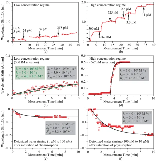
DL=KAi−1Δλw/(Δλmaxi−Δλw) (5) By substituting parameters in Table 2 into Eq. (5), DL with- out NS is estimated t o be 38 nM (=2.6μg/ml for BSA), while that with the NS, 255 fM (= 17 pg/ml). The real- time response of the spectral shift reflects the dynamic dif- fusion and adsorption of BSA. To observe this, we intermit- tently injected the solutions of different BSA concentrations from low to high using simple fluidic channels composed of glasses, plastics or PDMS polymer. All samples were manually injected by using a micro-pipette. Figure 10(a) focuses the response (sensorgram) in the low-concentration regime. Discontinuities just after injections were caused by the defocusing of pump light, which temporally stopped the lasing. We can observe a clear shift of 0.1–0.2 nm between 5 and 24 pM, which corresponds to ShiftL in Fig. 9(b). Al- though it is small at the injection of 36 pM, the response certainly exhibits a shift. From 36 pM to 1.6 nM, the irreg- ular step shift and gradual shift are mixed. It is considered to be due to the nonuniform distribution of BSA in the low-
Fig. 10 Sensorgrams for (a)–(d) adsorption and (e), (f) desorption of BSA. (a) and (b) exhibit the step-like shift due to intermittent injection of different concentration BSA for low and high concen- tration regimes, respectively. (c)–(f) show sensorgrams fitted with theoretical curves calculated with the Langmuir model considering diffusion of protein [43]. Used fitting parameters are denoted in each figure. (c) compares two fitting curves.
concentration regime and/or partially saturated adsorption at the NS. In the high-concentration regime, on the other hand, the step increase is observed more clearly in Fig. 10(b). The response is slower than the case in the low-concentration regime. To analyze the adsorption and desorption kinet- ics of BSA, we fitted theoretical curves, which were cal- culated with the Langmuir model considering the diffusion of protein [43], with the observed sensorgrams under dif- ferent situations. In the calculation, we also assumed fast protein diffusion such as 100μm/s, considering the force of the direct sample injection. Figure 10(c) shows the sen- sorgram in the low concentration regime. Here, two theo- retical curves were calculated for different dissociation rate constantskd of 1.0 ×10⁻⁴ s−1 and 3.0 ×10⁻³s−1, which
simulate the desorption from thin- and dense-adsorbed BSA [44], respectively (the adsorption rate constantkais given by KAkd). Then, we optimizedKAso that the theoretical curve fits to the experimental plots. It is seen in Fig. 10(c) that the round curve for largerkd fits better. The corresponding KAis 3.5×10¹¹M−1, which is almost comparable toKA1in Table 2 estimated for NS devices. Thus all the results con- sistently show that the dense adsorption actually occurred around the NS even in the low concentration regime. Fig- ures 10(d) and (e) show the adsorption and desorption in the high concentration regime, which should reflect the nor- mal chemisorption between GA and BSA. Both theoretical curves are in good agreement with experimental plots by setting the samekaandkd. Here,KA2=3.3×10⁷M−1was
Fig. 11 Sensorgrams of biotin-SA specific binding (red circle plots), which is compared with ph- ysisorption of SA (black circle plots). Red, black and green curves depict theoretical fits to biotin-SA specific binding, SA physisorption and the sum of both adsorption processes, respectively.
estiamted from the curve fitting, which is also on the same order as that in Table 2. The desorption behavior for the physisorption is also confirmed from Fig. 10(f), and aKA3 similar to that in Table 2 was also estimated.
We also tested the realtime sensing for the specific binding of biotin-SA, as shown in Fig. 11. Since such realtime specific binding of biomolecules has never been observed with nanolasers, we used high-concentration SA (2.8μM) in this preliminary experiment, and the result was compared with the case without biotin. After injecting SA, both cases exhibit the redshifts. The small redshift without biotin might be caused by the physisorption of SA on the device surface. The biotin-SA binding shows eight times larger shift, indicating that the specific binding is more dominant than the physisorption. Similarly to the results in Fig. 10, we can obtain fitting curves assuming KA and kd. When we only assumeKA =1.9×10¹³M−1 for the biotin-SA specific binding in Ref. [39] and a very smallkd
of 1.0×10⁻⁷min−1, the red curve in Fig. 11 was obtained, which does not fit to the experimental plots. It might be in- fluenced by the physisorption of SA simultaneously occur- ring due to the rapid increase in the SA concentration. In- deed, the green curve calculated from the sum of these two adsorption processes fits much better. The slight disagree- ment could be caused by the small difference of diffusion speed for each manual injection.
5. Conclusion
Nanolasers well satisfy the requirements of biosensing in terms of performance, cost and usability. By using photop- umped nanolaser as a sensor chip isolated from other equip- ments, its cost reduction and disposable use are possible.
We fabricated GaInAsP PC H0 nanolasers with a nanoslot of 30–60 nm width as a sensor chip. We observed the laser operation with a high yield even in water, which is suitable for biosensing. In particular, the nanoslot athermalized the
nanolaser in water and achieved a narrow spectrum, which is effective for high-resolution sensing. We applied this de- vice to the BSA protein sensing and unexpectedly evaluated a super-sensitivity. It gives an ultralow detection limit of 255 fM even assuming the worst intensity noise. This value is three orders of magnitude lower than that of SPR sensors reported recently [22]. The super-sensitivity was explained by the trapping of BSA in the nanoslot, to which the optical gradient force of localized laser mode contributes. We also demonstrated the detection of the biotin-streptavidin bind- ing as a preliminary experiment toward future specific de- tection of biomarkers in medical diagnoses. Further investi- gations of the trapping mechanism may lead to a unique con- trol tool for manipulating and detecting biomolecules more efficiently.
References
[1] Y.D. Ivanov, V.M. Govorun, V.A. Bykov, and A.I. Archakov, “Nan- otechnologies in proteomics,” Proteomics, vol.6, no.5, pp.1399–
1414, 2006.
[2] A. Van Den Berg and T.S.J. Lammerink, “Micro total analysis sys- tems: Microfluidic aspects, integration concept and applications,”
Microsystem Technology in Chemistry and Life Science, pp.21–49, 1998.
[3] S. Ray, H. Chandra, and S. Srivastava, “Nanotechniques in pro- teomics: Current status, promises and challenges,” Biosens. Bio- electron., vol.25, no.11, pp.2389–2401, 2010.
[4] J. Homola, S.S. Yee, and G. Gauglitz, “Surface plasmon resonance sensors: Review,” Sensors and Actuators B-Chemical, vol.54, no.1- 2, pp.3–15, 1999.
[5] J.J. Mock, D.R. Smith, and S. Schultz, “Local refractive index de- pendence of plasmon resonance spectra from individual nanoparti- cles,” Nano Lett., vol.3, no.4, pp.485–491, 2003.
[6] D.S. Grubisha, R.J. Lipert, H.Y. Park, J. Driskell, and M.D. Porter,
“Femtomolar detection of prostate-specific antigen: An immunoas- say based on surface-enhanced raman scattering and immunogold labels,” Anal. Chem., vol.75, no.21, pp.5936–5943, 2003.
[7] J.P. Kim, B.Y. Lee, S. Hong, and S.J. Sim, “Ultrasensitive car- bon nanotube-based biosensors using antibody-binding fragments,”
Anal. Biochem., vol.381, no.2, pp.193–198, 2008.
[8] J.P. Kim, B.Y. Lee, J. Lee, S. Hong, and S.J. Sim, “Enhancement of sensitivity and specificity by surface modification of carbon nan- otubes in diagnosis of prostate cancer based on carbon nanotube field effect transistors,” Biosens. Bioelectron., vol.24, no.11, pp.3372–
3378, 2009.
[9] Y. Ohno, K. Maehashi, and K. Matsumoto, “Label-free biosensors based on aptamer-modified graphene field-effect transistors,” J. Am.
Chem. Soc., vol.132, no.51, pp.18012–18013, 2010.
[10] C. Monat, P. Domachuk, and B.J. Eggleton, “Integrated optofluidics:
A new river of light,” Nature Photon., vol.1, no.2, pp.106–114, 2007.
[11] N.M. Hanumegowda, C.J. Stica, B.C. Patel, I. White, and X.D. Fan,
“Refractometric sensors based on microsphere resonators,” Appl.
Phys. Lett., vol.87, no.20, 201107, 2005.
[12] A.M. Armani, R.P. Kulkarni, S.E. Fraser, R.C. Flagan, and K.J.
Vahala, “Label-free, single-molecule detection with optical micro- cavities,” Science, vol.317, no.5839, pp.783–787, 2007.
[13] E. Krioukov, D.J.W. Klunder, A. Driessen, J. Greve, and C. Otto,
“Sensor based on an integrated optical microcavity,” Opt. Lett., vol.27, no.7, pp.512–514, 2002.
[14] K. De Vos, J. Girones, T. Claes, Y. De Koninck, S. Popelka, E.
Schacht, R. Baets, and P. Bienstman, “Multiplexed antibody de- tection with an array of silicon-on-insulator microring resonators,”
IEEE Photon. J., vol.1, no.4, pp.225–235, 2009.
[15] Y. Fang, A.M. Ferrie, N.H. Fontaine, J. Mauro, and J. Balakrishnan,
“Resonant waveguide grating biosensor for living cell sensing,” Bio- phys. J., vol.91, no.5, pp.1925–1940, 2006.
[16] M. Lee and P.M. Fauchet, “Two-dimensional silicon photonic crys- tal based biosensing platform for protein detection,” Opt. Express, vol.15, no.8, pp.4530–4535, 2007.
[17] R. Soref, “The past, present, and future of silicon photonics,” IEEE J. Sel. Top. Quantum Electron., vol.12, no.6, pp.1678–1687, 2006.
[18] S. Shinada, J. Hashizume, and F. Koyama, “Surface plasmon res- onance on microaperture vertical-cavity surface-emitting laser with metal grating,” Appl. Phys. Lett., vol.83, no.5, pp.836–838, 2003.
[19] M. Loncar, A. Scherer, and Y.M. Qiu, “Photonic crystal laser sources for chemical detection,” Appl. Phys. Lett., vol.82, no.26, pp.4648–
4650, 2003.
[20] S. Kita, S. Hachuda, K. Nozaki, and T. Baba, “Nanoslot laser,” Appl.
Phys. Lett., vol.97, no.16, 161108, 2010.
[21] S. Kita, K. Nozaki, S. Hachuda, H. Watanabe, Y. Saito, S. Otsuka, T. Nakada, Y. Arita, and T. Baba, “Photonic crystal point-shift nanolaser with and without nanoslots — Design, fabrication, lasing and sensing characteristics,” IEEE J. Sel. Top. Quantum Electron., vol.17, pp.1632–1647, 2011.
[22] W.C. Law, K.T. Yong, A. Baev, R. Hu, and P.N. Prasad, “Nanopar- ticle enhanced surface plasmon resonance biosensing: Application of gold nanorods,” Opt. Express, vol.17, no.21, pp.19041–19046, 2009.
[23] A. Densmore, M. Vachon, D.X. Xu, S. Janz, R. Ma, Y.H. Li, G. Lopinski, A. Delage, J. Lapointe, C.C. Luebbert, Q.Y. Liu, P.
Cheben, and J.H. Schmid, “Silicon photonic wire biosensor array for multiplexed real-time and label-free molecular detection,” Opt.
Lett., vol.34, no.23, pp.3598–3600, 2009.
[24] N. Skivesen, A. Tetu, M. Kristensen, J. Kjems, L.H. Frandsen, and P.I. Borel, “Photonic-crystal waveguide biosensor,” Opt. Express, vol.15, no.6, pp.3169–3176, 2007.
[25] S. Zlatanovic, L.W. Mirkarimi, M.M. Sigalas, M.A. Bynum, E.
Chow, K.M. Robotti, G.W. Burr, S. Esener, and A. Grot, “Photonic crystal microcavity sensor for ultracompact monitoring of reaction kinetics and protein concentration,” Sens. Act. B Chem., vol.141, no.1, pp.13–19, 2009.
[26] K. Nozaki, S. Kita, and T. Baba, “Room temperature continuous wave operation and controlled spontaneous emission in ultrasmall photonic crystal nanolaser,” Opt. Express, vol.15, no.12, pp.7506–
7514, 2007.
[27] S. Kita, K. Nozaki, and T. Baba, “Refractive index sensing utilizing
a CW photonic crystal nanolaser and its array configuration,” Opt.
Express, vol.16, no.11, pp.8174–8180, 2008.
[28] S. Kita, Y. Nishijima, H. Misawa, and T. Baba, “Label-free biosens- ing utilizing ultrasmall photonic crystal nanolaser,” OSA Integrated Photon. Nanophoton. Res. Appl. Top. Meet., no.JMB3, 2009.
[29] H. Watanabe, K. Nozaki, and T. Baba, “Very wide wavelength chirp- ing in photonic crystal nanolaser,” Int. Sympo. Compound Semicon., no.TuC P-10, 2007.
[30] T.W. Lu, P.T. Lin, K.U. Sio, and P.T. Lee, “Optical sensing of square lattice photonic crystal point-shifted nanocavity for protein adsorp- tion detection,” Appl. Phys. Lett., vol.96, no.21, 213702, 2010.
[31] Q.F. Xu, V.R. Almeida, R.R. Panepucci, and M. Lipson, “Experi- mental demonstration of guiding and confining light in nanometer- size low-refractive-index material,” Opt. Lett., vol.29, no.14, pp.1626–1628, 2004.
[32] J.T. Robinson, C. Manolatou, L. Chen, and M. Lipson, “Ultrasmall mode volumes in dielectric optical microcavities,” Phys. Rev. Lett., vol.95, no.14, 143901, 2005.
[33] A.H.J. Yang, S.D. Moore, B.S. Schmidt, M. Klug, M. Lipson, and D.
Erickson, “Optical manipulation of nanoparticles andbiomolecules in sub-wavelength slot waveguides,” Nature, vol.457, no.7225, pp.71–75, 2009.
[34] A. Di Falco, L. O’Faolain, and T.F. Krauss, “Chemical sensing in slotted photonic crystal heterostructure cavities,” Appl. Phys. Lett., vol.94, no.6, 063503, 2009.
[35] D.W.K.F. Palmer, “Optical properties of water in the near infrared,”
J. Opt. Soc. Am., vol.64, pp.1107–1110 1974.
[36] D.R. Lide, CRC handbook of chemistry and physics, 82nd ed., pp.10–218, CRC Press, 2001.
[37] C. Silva, F. Sousa, G.G. Bitz, and A. Cavaco-Paulo, “Chemical mod- ifications on proteins using glutaraldehyde,” Food Technology and Biotechnology, vol.42, no.1, pp.51–56, 2004.
[38] N.M. Green, “Avidin and streptavidin,” Methods in Enzymology, vol.184, pp.51–67 1990.
[39] D.E. Hyre, I. Le Trong, E.A. Merritt, J.F. Eccleston, N.M. Green, R.E. Stenkamp, and P.S. Stayton, “Cooperative hydrogen bond in- teractions in the streptavidin-biotin system,” Protein Science, vol.15, no.3, pp.459–467, 2006.
[40] M. Noto, D. Keng, I. Teraoka, and S. Arnold, “Detection of pro- tein orientation on the silica microsphere surface using transverse electric/transverse magnetic whispering gallery modes,” Biophysi- cal Journal, vol.92, no.12, pp.4466–4472, 2007.
[41] H.-J. Butt, K. Graf, and M. Kappl, Physics and chemistry of inter- faces, pp.191–199, Wiley-VCH, 2003.
[42] K. Shigemori, S. Nishizawa, T. Yokobori, T. Shioya, and N.
Teramae, “Selective binding of very hydrophilic h2po4- anion by a hydrogen-bonding receptor adsorbed at the 1, 2-dichloroethane- water interface,” New J. Chem., vol.26, no.9, pp.1102–1104, 2002.
[43] D.X. Xu, A. Densmore, A. Delage, P. Waldron, R. McKinnon, S.
Janz, J. Lapointe, G. Lopinski, T. Mischki, E. Post, P. Cheben, and J.H. Schmid, “Folded cavity SOI microring sensors for high sen- sitivity and real time measurement of biomolecular binding,” Opt.
Express, vol.16, pp.15137–15148, 2008.
[44] H. Urano and S. Fukuzaki, “Conformation of adsorbed bovine serum albumin governing its desorption behavior at alumina-water inter- faces,” J. Biosci. Bioeng., vol.90, pp.105–111, 2000.
Shota Kita received the B.E. and M.E.
degrees from the Department of Electrical and Computer Engineering, Yokohama National University, Yokohama, Japan, in 2007 and 2009, respectively. He is currently working towards the Ph.D. degree in photonic crystal nanolasers and their applications for liquid and biosensing at the same university. Mr. Kita is a member of the Japan Society of Applied Physics. He received two academic awards including JSAP presentation award in 2010.
Shota Otsuka received the B.E. degree from the Department of Electrical and Com- puter Engineering, Yokohama National Univer- sity, Yokohama, Japan, in 2011. He is currently working towards the M.E. degree in ultra high sensitivity photonic crystal nanolaser biosensor at the same university. Mr. Otsuka is a member of the Japan Society of Applied Physics.
Shoji Hachuda received the B.E. degree from the Department of Electrical and Com- puter Engineering, Yokohama National Uni- versity, Yokohama, Japan, in 2010. He is currently working towards the M.E. degree in bio-electronics and surface chemistry and photonic crystal nanolaser biosensor for bio- marker protein detection at the same university.
Mr. Hachuda is a member of the Japan Society of Applied Physics.
Tatsuro Endo received his Ph.D. degree from the Japan Advanced Institute of Science and Technology (JAIST), Biotechnology Lab- oratory in the Dept. of Biological Science and Biotechnology, in 2006. He was an assistant professor at P&I Lab of Tokyo Institute of Tech- nology in 2006–2011. Then he became an as- sociate professor at the Department of Applied Chemistry, Osaka Prefecture University. His current field of interest includes nanophotonics, biophotonics and nanobiotechnology.
Yasunori Imai received the B.E. degree from the Department of Bioengineering, Tokyo Institute of Technology, Japan, in 2010. He is currently working towards the M.E. degree in SiN photonic crystal and their applications for sensing bio-molecules at the same university.
Yoshiaki Nishijima received the B.E.
degree from the Facility of Science Division of Chemistry, Hokkaido University, in 2004, M.D. degree from Graduate School of Science, Hokkaido University in 2006, and Ph.D. degree from Graduated School of Information Science, Hokkaido University in 2009. During his Ph.D.
work, he had been engaged in fabrication and characterization of opal photonic crystals. From 2009 to 2010, He worked as a postdoctrate fel- low at Research Institute for Electronic Science, Hokkaido University, working on the plasmonic solar cell. He became an assistant professor at Yokohama National University in 2011. His recent study is focusing on material science and chemistry especially for visible to THz wavelength plasmonic materials. Dr. Nishijima is a member of the Japan Society of Applied Physics and Chemical Society of Japan.
Hiroaki Misawa is Director and Professor at the Research Institute for Electronic Science, Hokkaido University, Sapporo, Japan. He ob- tained his B.Sc. in Engineering from the Depart- ment of Engineering at Tokyo Metropolitan Uni- versity in 1979, graduated in Engineering from the University of Tsukuba in 1981 and com- pleted his Ph.D. at the Department of Chemistry there in 1984. After postdoctoral positions at the Universities of Texas at Dallas and an Assistant Professorship at the University of Tsukuba, he joined the Department of Engineering of University of Tokushima in 1993 and was promoted to full professor in 1995. His current research inter- ests include light-matter interaction, ultra-fast processes in materials, plas- monics, and strong photon-molecule coupling fields for chemical reaction.
He authored more than 260 papers. He was the representative researcher of Core Research for Evolutional Science and Technology by Japan Sci- ence and Technology Corporation from 2003 to 2007. He had engaged in Grant-in-Aid for Scientific Research (KAKENHI) on Priority Area enti- tled “Strong Photon-Molecule Coupling Fields for Chemical Reactions”, MEXT, Japan from 2007 to 2011. He is Deputy Editor of the Journal of Photochemistry and Photobiology C, Photochemistry Review and a mem- ber of ACS Journal of Physical Chemistry C Advisory Board.
Toshihiko Baba received the Ph.D. de- gree from the Division of Electrical & Com- puter Engineering, Yokohama National Univer- sity (YNU), Japan, in 1990. During his Ph.D.
work, he had been engaged in ARROW waveg- uides and photonic integration. From 1991–
1993, he joined Tokyo Institute of Technol- ogy as a research associate and investigated the spontaneous emission control and room temper- ature cw operation in VCSELs. He became an associate professor and full professor of YNU in 1994 and 2005, respectively. In these 18 years, he has studied pho- tonic nanostructure devices including photonic crystals (PCs), microdisks, and Si photonics devices. His recent topics are regarding slow light PC waveguides towards tunable delay, nonlinear enhancement, and high-speed modulators, Si photonics devices and circuits based on CMOS-compatible process, and bio-sensing using PC nanolasers. He is an author of 150 jour- nal papers with more than 5200 citations. Dr. Baba is a member of IEICE, JSAP, IEEE/Photonics, OSA, and APS, and an associate member of Sci- ence Council of Japan. He received 10 academic awards including JSPS Award in 2005, IEEE/LEOS Distinguished Lecturer Award in 2007, and IEICE Electronics Society Award in 2011.