Japan Advanced Institute of Science and Technology
JAIST Repository
https://dspace.jaist.ac.jp/
Title 有機電界効果トランジスタを用いたマルチレベルメモ
リに関する研究
Author(s) Tran, Cuong Manh Citation
Issue Date 2017‑09
Type Thesis or Dissertation Text version ETD
URL http://hdl.handle.net/10119/14835 Rights
Description Supervisor:村田 英幸, マテリアルサイエンス研究科
, 博士
- i -
Acknowledgement
This study could not able to be completed without the help and contribution of many people. I would like to express my deepest gratitude to my supervisors, Professor Hideyuki Murata, School of Material Science, Japan Advanced Institute of Science and Technology (JAIST) for their valuable suggestions, their kind encouragements, supervision and great supports throughout my doctoral study. I have been encouraged in actualizing the challenging ideas and promoted to present my studies at scientific publications as well as in many conferences in Japan and around the world.
I deeply appreciate and thank my all the committee members, Professor Masahiko Tomitori, Professor Toshi-kazu Suzuki, Professor Eisuke Tokumitsu, in JAIST and Professor Eunsang Kwon in Tohoku University for their participation in the review and evaluation of this work.
My thanks would like to give Assistant Professor Heisuke Sakai for his teaching and his assistance in the daily work. He reviewed and gave me many useful comments during my preparation for my scientific writing and my dissertation. In addition, I would like to express many thanks to members of Murata Lab for their helps in my experimental activities and my daily life. I have learned so much from all of them.
My thanks would like to go to The Ministry of Education, Culture, Sports, Science and Technology (MEXT) for financial support to study in Japan.
Finally, I profoundly appreciate the encouragement, understanding and support from my parents, my wife, my daughters and all my friends at JAIST.
- ii - Contents
Acknowledgement ... i
List of Symbols ... v
List of Abbreviations ... vi
CHAPTER 1 || INTRODUCTION ... 1
1.1. Electrical memory ... 1
1.2. Organic memory ... 3
1.3. Organic multi-level cell memories ... 12
1.4. Summary of current issues of the MLC organic memory ... 14
1.5. Aims of study ... 15
Reference ... 18
CHAPTER 2 || AN EFFECT OF BACKGROUND PRESSURE ON THE PERFORMANCE OF MEMORY OFETS FOR MLC DEVICES ... 22
2.1. Introduction ... 23
2.2. Experimental ... 25
2.3. Basic parameters of OFETs ... 27
2.4. Effect of background pressure on a contact resistance reduction ... 31
2.5. An origin of the reduction of contact resistance ... 32
2.6. Conclusions ... 35
Reference ... 36
CHAPTER 3 || WRITE-ONCE-READ-MANY MLC MEMORY OFETS USING POLY (VINYL CINAMMATE) AS CHARGE TRAPPING LAYER ... 38
3.1. Introduction ... 39
3.2. Experimental ... 41
3.3. Basic parameters of OFETs ... 43
3.4. MLC memory properties of OFETs ... 45
- iii -
3.4.1. MLC memory effect ... 45
3.4.2. Stability of logic states ... 46
3.4.3. Retention characteristics ... 47
3.5. Mechanism discussions ... 48
3.6. Conclusion ... 52
Reference ... 53
CHAPTER 4 || MLC ORGANIC MEMORY TRANSISTOR USING LITHIUM- ION-ENCAPSULATED FULLERENE AS CHARGE TRAPPING LAYER ... 55
4.1. Introduction ... 56
4.2. Experimental ... 58
4.3. Basic parameters of OFETs ... 60
4.4. MLC memory properties of OFETs ... 62
4.4.1. Shift of the Vth under programmed/erased conditions ... 62
4.4.2. Reproducibility of logic states... 63
4.4.3. Retention time characteristics ... 64
4.5. Proposed operation mechanism ... 65
4.6. Conclusion ... 69
Reference ... 70
CHAPTER 5 || OPERATION MECHANISM OF MLC MEMORY OFETS USING LITHIUM-ION-ENCAPSULATED FULLERENE AS CHARGE TRAPPING LAYER ... 72
5.1. Introduction ... 73
5.2. Trapped electrons in a single Li+@C60 molecule ... 75
5.3. Evidence of electron trapping in the Li+@C60 layer ... 80
5.4. Migration of Li+@C60 molecule into the pentacene layer ... 84
5.5. Conclusion ... 86
Reference ... 87
- iv -
CHAPTER 6 || CONCLUSION AND FUTURE WORK ... 88 6.1. Conclusions ... 88 6.2. Future work ... 91
- v - List of Symbols
Symbols Meaning
µ Mobility
ΔVth Memory window
ΔGet The driving force of electron transfer
A Area if capacitor device
d Thickness of insulator in a capacitor
e Elementary charge
ID Drain current
ID,sat Saturation drain current
IG Gate current
J Current density
L Channel length
N Number of trapped electron
P Number of trapped hole
P/E Programming/Erasing
V Voltage
VD Drain voltage
VG Gate voltage
Vth Threshold voltage
W Channel width
- vi - List of Abbreviations
Abbreviations Meaning
AFM Atomic force microscopy
CD Compact disc
CNT Carbon nanotube
CPU Central processing unit
CuPc Copper phthalocyaine
CYTOP Poly-perfluoro-alkenyl vinyl ether
D Drain electrode
DRAM Dynamic Random Access Memory
EPROM Electrically programmable Read Only Memory EEPROM Electrically erasable programmable Read Only
Memory
F8BT Poly(9,9-di-n-octylfluorene-alt- benzothiadiazole)
FeRAM Ferroelectric Random Access Memory
G Gate electrode
HOMO Highest occupied molecular orbital
IPA Isopropyl alcohol
ITO Indium tin oxide
LUMO Lowest unoccupied molecular orbital
MIM Metal/Insulator/Metal
MIS Metal/Insulator/Semiconductor
MLC Multi-level cell
NPs Nanoparticles
OFET Organic field effect transistor OLED Organic light-emitting diode
P4MS Poly (4-methyl styrene)
PMMA Poly (methyl methacrylate)
PS Polystyrene
PVA Poly (vinyl alcohol)
- vii -
P(VDF-TrFE) poly (vinylidene fluoride-co-trifluoroethylene)
PVN Poly (2-vinyl naphthalene)
PVP Poly (4-vinyl phenol)
PVPyr Poly (2-vinnyl pyridine)
PQ Poly quinoline
PαMS Poly (α-methylstyrene)
RAM Random access memory
ROM Read only memory
S Source electrode
SAM Self-assembled monolayer
SCS 4200 Keithley 4200 semiconductor characterization
SLC Single-level cell
SRAM Static Random Access Memory
star-PTPMA star-shaped poly((4-diphenylamino) benzyl methacrylate
UPS Ultraviolet photoelectron spectroscopy UV-Vis Ultraviolet-visible spectroscopy UV-O3 Ultra-violet ozone surface treatment
WORM Write-once-read-many
XPS X-ray photoelectron spectroscopy
- 1 -
CHAPTER 1 || INTRODUCTION
1.1. Electrical memory
An electronic memory plays an important role in the operation of electronic devices such as mobile phones, personal computers, camera, music players. The memory or the storage is defined as a component or device that retains retrievable digital data over a time interval.1 For the operation, the memory is connected to a central processing unit (CPU). Then data stored in the memory can be read or written by the CPU. Memory can be classified based on a method to connect to CPU and a response. A cache memory integrated inside the CPU has the highest access speed.
The cache memory is used as a buffer to transfer data from/to an internal memory.
The internal memory, which is connected to the CPU via system bus with high speed, stores all the data of the system for its operation. External memories such as floppy disk, hard disk, compact disc (CD) or a digital versatile disc or digital video disc (DVD) are portable storages, which can be used whenever they are connected. To enhance the performance of the electronic systems, a development of memories is essential.
Electrical memories also can be divided into non-volatile and volatile memories based on the duration of stored data when an electric supply power is turned off. The data stored in non-volatile memories could be remained for a certain time, while it stored in volatile memories would loss immediately. Further classification of electrical memories was reported2-3, which is shown in Fig.1.1. ROM (Read Only Memory) including EPROM (Electrically Programmable ROM)4 and WORM3-5 (Write-once-read-many) could hold the data permanently after being written only
- 2 -
once and the stored data cannot be modified. Thus, this type of memory is often used to store the passive data in which the data are kept and made it available for the long- term use, such as Bios program in a computer. The flash, EEPROM (Electrically erasable programmable ROM) and FeRAM (Ferroelectric Random Access Memory) keep the data for a long time, and the data stored in them can be programmed or erased many times3,6-10. These memories are non-volatile and rewritable. These can be used for portable devices, for instance a portable music player and an USB (Universal Serial Bus) disk. The last forms of memory, RAM (Random Access Memory) including DRAM (Dynamic RAM) and SRAM (Static RAM) are often used for the memory of the computer system. The data in RAM can be programmed/erased many times with a high access speed. However, the data are lost when no electrical power is supplied.
Fig.1.1. Classification of electrical memories
- 3 - 1.2. Organic memory
The organic memory consists of carbon-based materials, including small molecules and polymers. There are many researches on the organic memory due to its advantages such as low temperature fabrication process, solution process ability or printability, a flexibility of devices, and low cost. Those are suitable for large area fabrication2-10.
A classification of organic memories is based on a typical structure of the memory devices, of which organic memories can be divided into capacitor-, resistor- and transistor-based memory.
1.2.1. Capacitor-based memories
A capacitor-based memory has a structure of an insulator layer sandwiched between two electrodes. Based on the material for electrodes, there are two structures of capacitor-based memories: Metal/Insulator/metal (MIM) structure, and Metal/Insulator/Semiconductor (MIS) structure.
Fig.1.2. (a) Device structure, (b) polarization, (c) de-polarization, (d) capacitance- voltage, (e) charge displacement of a MIM memory
- 4 -
In the MIM memory as shown in Fig.1.2 (a), both electrodes are made from metals while the insulator is ferroelectric material11. By applying an external bias voltage, the ferroelectric layer is polarized (Fig.1.2 (b)) or depolarized (Fig.1.2 (c)) causing a hysteresis in a capacitance-voltage curve (Fig.1.2 (d)) or a charge displacement-electric field curve (Fig.1.2 (e))12-14. To program or write the data into the MIM memory, a required voltage of +VCC or -VCC is applied between electrodes, resulting in two stable states of the device, where upward polarization and downward polarization could be defined as a signal of “1” and “0”, respectively13. To read the data in the MIM memory, a nearly zero voltage is applied. Electric field caused the polarization (depolarization) of ferroelectric layer, would increase (decrease) the bias voltage between the electrodes. This is detected and referred to the signal of “1”
(“0”)15.
Fig.1.3. (a) Ferroelectric, (b) charge trapping, (c) floating gate structure, (d) capacitance-voltage curve of a p-type MIS memory.
- 5 -
The structure of the MIS memory is shown in Fig. 1.3 (a)-(c). When a high voltage is applied between electrodes, charges are injected from the top electrode, and then accumulated in a semiconductor layer. When a negative voltage is applied to the bottom electrode of a p-type MIS capacitor which is shown in Fig. 1.3b, the capacitor is in the accumulation case. The holes are increased at the surface of the semiconductor, and somehow could be trapped at the trapping layer. When the voltage is sweeping to small positive voltage, the MIS capacitor is not in the depletion case because the applied electric field is still smaller than that caused by the trapped holes.
To get into to the depletion case and the inversion case, the MIS capacitor required higher applied voltage compared with the device without trapping layer. As the results, the capacitance-voltage (C-V) curve shifts to the positive region of applied voltage (the blue line in Fig. 1.3d). At high applied positive voltage, the trapped holes could be de-trapped. In addition, the electrons could be trapped at the charge trapping layer due to the high density of electrons at the semiconductor surface. In the case of reversed curve, because of the trapped electrons, the MIS memory will get into depletion case at negative applied voltage. And higher negative voltage is required to get into the accumulation case. Thus, the C-V curve shifts to the negative region (the red line in Fig. 1.3d). When high positive voltage is applied, the trapped electrons will be de-trapped and then holes will be trapped. The trapped holes make the C-V curve shift to positive region while the trapped electrons make it shift to the negative region.
The hysteresis of the C-V curve of the MIS capacitor caused by the charge trapping relates to the memory effect of the device. The memory window of the MIS memory is calculated to be the difference of the flat-band between the forward and the reversed C-V curves. The difference capacitance of the MIS in the forward and backward curves refers to the logic signal of “1” or “0” of the stored data. The data can be lost when the memory is set in the depletion state.
1.2.2. Resistor-based memories
A memory based on resistor simply consists of an active layer between two electrodes (MIM structure) on a supporting substrate of plastics, glass metal foil (Fig.
1.4 (a)). Electrodes are mostly made from aluminum (Al), gold (Au), copper (Cu), or
- 6 -
n-doped silicon (n-doped Si) and indium tin oxide (ITO). For the active layer, materials are small molecules, polymers, composite of polymer and molecules, nanoparticles (NPs) or some biomacromolucules16-19. Fig. 1.4 (b) and (c) show the current-voltage (I-V) curves of a WORM and the rewritable resistor-based memory.
The operation of the memory devices is based on the change of the conductivity of the active layer corresponding to the applied voltage. At a programming voltage of Vth (or +Vth1), the current changes from low to high, corresponding to the data of “1”, which is distinguished from the data of “0”. In the rewritable device, the stored data can be erased when a negative voltage of -Vth2 is applied.
There are many operation mechanisms to explain the switching of the conductivity in the resistor memory. These mechanisms can be explained by the thermal, electronic, and electrochemical effects16,20. For the thermal effect, the crystalline state or the amorphous state at different temperatures determines the conductivity of the active layer, resulting in the change of the states of the memory21,22. On the other hand, the conductivity switching could be occurred by the electronic effect. Under a high electric field, charges are injected by Fowler-Nordheim tunneling and trapped at defects or metal nanoparticles in the insulator, resulting in the change in the resistance of the active layer23-26. Or electronic injected charges can act like a dopant which causes to an insulator-metal transition in perovskite-type oxides, correlates to the switching27-29. The third group of switching mechanism is based on the electrochemical effect, in which the migrations of cations30 or anions31 from electrodes to the active layer occur. These migrations correspond to the change of conductivity of the active layer.
Fig.1.4. (a) A typical structure of a resistor memory, and the I-V curve of (b) a WORM or (c) a rewritable memory.
- 7 - 1.2.3. Transistor-based memories
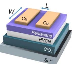
Both the capacitor- and the resistor-based organic memories require an external transistor for their operations while an organic field effect transistor (OFET)- based memory does not require3,4,16. Because of this advantage, this study focuses only on the OFET memory. Fig. 1.5 shows typical structures of the OFET memory including a ferroelectric transistor memory, a floating gate transistor memory, and a charge trapping transistor memory.
The ferroelectric transistor memory (Figure 1.5. (a)), which was proposed in the 1950s32. The ON and OFF states of the memory are obtained by a polarization or depolarization of the ferroelectric gate layer32-35. A material commonly used for the ferroelectric layer is poly (vinylidene fluoride-co-trifluoro ethylene) (P(VDF-TrFE)) because of its wide bandgap. As the result, the memory using P(VDF-TrFE) does not require another gate insulator33. Based on this material, Naber et al, reported a ferroelectric transistor memory with an ON/OFF ratio of 105, a retention characteristic up to one week, high programming cycle endurance of 1000 cycles, a short programming time of 0.5 ms, and the programming/erasing voltages of ±35 V34,35. To improve the performance of the ferroelectric transistor memory, the reduction in the operation voltages, and the short programming duration, as well as the long retention characteristics are significant.
Reported by Kahng and Sze in 1967, a floating gate transistor could be used as a non-volatile memory36. By applying a voltage to the gate, charges were injected from the source/drain (S/D) electrodes and then trapped in the floating gate. These trapped charges affect to the charge carriers in the channel, causing the change in the drain current (ID) and the shift of the threshold voltage (Vth) of the OFETs (Fig. 1.5.
(b)). Since the trapped charges in the floating gate are blocked by the insulator, the change in the ID and the shift of the Vth will remain unchanged, corresponding to the memory effect. For erasing the memory, a reversed voltage is applied to the gate, removing the charges from the floating gate. The floating gate could be made from a thin layer of metal such as aluminum37,38. These memories exhibited excellent memory characteristics with an operation voltage of lower than 6 V, a large memory window (ΔVth) of 2.4 V, retention time of 105 seconds and a stable Vth after 103 program-erase cycles. However, a fabrication process of this memory transistor
- 8 -
required complicated technique. Another method for a floating gate fabrication is using nanoparticles. In 2003, Kolliopoulou et al. reported a memory transistor using gold nanoparticles (AuNP) as the floating gate separated from the Al gate electrode by an insulator, which was made by Langmuir-Blodget technique39. The excellent characteristics of the memory were observed with the low operation and programming/erasing voltages of 6 V. Up to now, many efforts to make the fabrication process of Au NP-floating gate memory more simply were reported by Z. Liu et al.40, W. Wang et al, S.-J. Kim et al.41, and K.-J. Baeg et al.42
The operation of a charge trapping memory transistor is similar to that of the floating gate memory, of which the charges are injected from the S/D electrodes and trapped at the dielectric layer (Fig. 1.5 (c)). The trapped charges affect to charge
Fig.1.5. A typical structure of (a) a ferroelectric transistor memory (b) a floating gate transistor memory, and (c) a charge trapping transistor memory.
- 9 -
carriers in the channel of the OFETs causing the change in the ID and the shift of the Vth, which is related to the memory effect. The first charge trapping memory OFET was reported in 2002 by H.E. Katz et al.43, and then many other research groups started to focus on this topic. Baeg et al. reported a pentacene-based memory OFET using poly(α-methylstyrene) (PαMS) as a charge trapping layer fabricated on a layer of SiO2 44. This memory showed a large ΔVth of 90 V as well as a long retention time up to 100 h, but it required high programming/erasing voltages of 200/-100 V. Beside the use of PαMS for charge trapping layer44,49, some other materials were used such as polystyrene (PS)45, poly (4-methyl styrene) (P4MS)45, poly (2-vinyl naphthalene) (PVN)45, poly (4-vinyl phenol) (PVP)45, poly (2-vinnyl pyridine) (PVPyr)45, poly (vinyl alcohol) (PVA)45,46, poly(methyl methalcrylate) (PMMA)47, and poly (perfluoroalkenyl vinyl ether) (CYTOP)48. The charge trapping memory OFETs have an advantage of the simple structure and facile fabrication process. Therefore, we utilized this structure to fabricate our devices.
Fig.1.6. (a) the top view, (b) cross section of top-contact p-channel OFET and (c) its typical transfer and (d) the ΔVth definition of the memory.
- 10 - Basic parameters of the OFET memory
Technical parameters of an organic field effect transistor were described in the IEEE Standard 1620-200450 and the IEEE Standard 1005-199851, which were summarized in Fig. 1.6, the table 1.1, and 1.2 as bellows:
Table 1.1. Definitions Definition Meaning
W The width of the channel (Fig. 1.6 a) L The length of the channel (Fig. 1.6 a)
IDS (ID) The current flow measured through the drain electrode IGS (IG) The current flow through the gate dielectric, leakage
current
VDS (VD) The voltage applied to the drain electrode VGS (VG) The driven voltage applied to the gate electrode
Transfer curve Measurement where ID is measured as a VG swept from a start voltage to a stop voltage (Fig. 1.6 c)
Output curve ID vs. VDS for a fixed VGS
µ Mobility is the majority carrier mobility of semiconductor material derived through transfer curve
Vth (VT) Threshold voltage is the minimum gate voltage required to induce the channel (Fig. 1.6 c)
On/off ratio The maximum ID value divided by the minimum ID value, obtained from the transfer curve
Program/erase voltages
The voltages applied to the gate to make the states of the memory change
Switching time The duration of program/erase voltages
ΔVth Memory window is defined by the difference in Vth
between the programmed and erased states (Fig. 1.6 d) Retention Time from data storage to the time at which a veritable
error is detected from any cause.
Endurance Number of program/read/erase/read cycles
- 11 - Table 1.2. Device structure
Definition Meaning
Bottom-contact An OFET structure where the S and D electrodes are located closer to the substrate than the semiconductor.
Bottom-gate An OFET structure where the gate electrodes are located closer to the substrate than the semiconductor.
- 12 - 1.3. Organic multi-level cell memories
Along with the development of electronic devices, both the size and the mass of them are needed to reduce. Moreover, their operation should be stronger with a lower power consumption. The memory, which is an essential part of the computer system, also should be smaller with high volume. Thus, an increase in the capacity of storage has been attractive attentions, resulting in the development of a multi-level cell (MLC) memory. A MLC memory or a MLC per cell storage differentiate from a single-bit memory or a single level cell storage (SLC) at the capacity of storage. R.
Michelroni et al, showed his definition of a SLC memory and a MLC memory in his textbook.52 A SLC memory distinguishes between “1” and “0” by having no charge or charge present on the floating gate of the memory cell. By increasing the number of charge in the floating gate or Vth levels, more than 1 bit of data per cell may be stored
MLC requires accurate placement of the Vth level so that the charge distribution do not over-lap. Another requirement for the accurate sensing of the different charge level. These requirements ensure the replication of the logic states after the programming/erasing repetition. To satisfy requirements above, the polarization of the ferroelectric layer in the ferroelectric memory or the quantity of the trapped charges in NPs or the trapping layer must be controlled perfectly. Thus, a few of researches on the MLC organic memory have been published 53-61.
Despite containing several states, a structure of the MLC memory is not different from that of the single-bit memory. It means that the MLC memory structure is also based on a resistor53,54, a capacitor55,56, or a transistor57-61. The MLC memory based on a resistor was reported by Hwang et al in 2012 using doped-carbon nanotubes (CNTs) as an electron trapping material combined with PS. Excellent memory characteristics were observed in the devices under a low operation voltage of -1 V.
Recently in 2016, Lee et al. reported another MLC resistor memory using a mix of Poly(9,9-di-n-octylfluorene-alt-benzothiadiazole) (F8BT) and P(VDF-TrFE) as a main part of an active layer54. Although this memory exhibited 4 logic states, it had a poor retention time of only 1,000 seconds and a low on/off ratio of about 102. The ferroelectric material of P(VDF-TrFE) was used not only for the capacitor-based55,56 but also for the transistor-based MLC memories57,58. The capacitor-based memory
- 13 -
reported by Kim et al.55 exhibited an excellent performance with an operation voltage of lower than 20 V, expected retention time of 10 years, and showed 1,800 cycles of endurance measurement. Moreover, a model of the capacitor-based memory was given by Khikhlovskyi et al. could store 3 bits of data56. In terms of the transistor- based memory, ferroelectric MLC devices were introduced by Tripathi et al. in 201157, Khan et al. in 201558. Common characteristics of P(VDF-TrFE)-based memory OFET were a low operation and programming voltages of lower than 30 V, but the retention time was only 104 seconds.
Regarding to the concept of the charge trapping memory, Guo et al. reported a MLC OFET using pentacene or copper phthalocyaline (CuPc) as an active material and PS or PMMA as a charge trapping layer59. Under a drain voltage (VD) of -60 V, the memory OFET showed several ON states after programming by applied voltages of 80 V with an assisted-light resource. This disadvantaged feature would limit applications of this device, although it exhibited a high on/off ratio and long retention characteristics compared with the ferroelectric MLC memory OFETs. In 2013, Chiu et al. reported a charge trapping MLC memory OFET, which used a material of a star- shaped poly((4-diphenylamino) benzyl methacrylate (star-PTPMA) for the charge storage and N,N’-bis(2-phenylethyl)perylene-3,4,9,10-bis(dicarbonximide) for a n- type channel60. This device operated with a high programming voltage of 200 V, and exhibited a write-once-read-many memory, of which those data could not be erased.
Recently, in 2016, another MLC memory OFET was introduced using a new material of polyquinoline (PQ). The layer of PQ is ascribed to trap electrons, which causes the hysteresis in the transfer curve, corresponds to the MLC effect in this OFET61. In spite of some limitation such as high operation and programming voltages, disability to erase the stored data, this result was still a positive sign for the application of the new material in the MLC memory OFET.
To deeply understand about the MLC memory organic devices, some issues of them were listed and summarized in the next section in this chapter.
- 14 -
1.4. Summary of current issues of the MLC organic memory
Based on a few researches on the MLC organic memory, some current issues are summarized and shown in the table 1.3. The most significant issue of the organic MLC memory is the shortage of desired materials. Almost memory devices were fabricated using P(VDF-TrFE). These memories exhibited an excellent performance.
In the case of the charge trapping MLC memory OFETs, only polymers of PS and PMMA were used. It inspires us to investigate different polymers as the charge trapping layer for the devices. In addition, the use of a new material for charge trapping layer is expected to open a new trend of the research in these kinds of the devices.
Table 1.3. Summary of current issues in the organic MLC memory Characteristics Resistor-
based memory
Capacitor- based memory
Transistor-based memory Ferroelectric Charge trapping
Structure 1T-1R 1T-1C 1T 1T
Key material P(VDF- TrFE) Doped- CNT
P(VDF-TrFE) P(VDF-TrFE) PS, PMMA, star-PTPMA,
PQ Operation
voltage
< 20 V -1 V
< 20 V < 30 V 60 V 100 V Programming
conditions
18.5 V 3 V
8 V 30 V, or 80 V with light, 200 V, 100 V Retention 1,000 s Up to 10 years 3,500 seconds 20,000 seconds
- 15 - 1.5. Aims of study
Because the MLC memory using P(VDF-TrFE) exhibited an excellent performance, subjects of this dissertation are to focus on the charge trapping structure of devices with a semiconductor of pentacene. Because of the high programming and operation voltages in the charge trapping memory OFETs, I proposed the aims of this study are:
• A method to increase a performance (mobility) of the OFET, which could be applied to the memory OFET.
• Reduction of operation voltage
• Reduction of programming voltage
To archive these aims, I applied the new material of poly (vinyl cinnamate) and Lithium-ion-encapsulated fullerene as the charge trapping layer. Fig. 1.7 shows the structure of this dissertation, which main achievements were summarized as follows:
The first achievement is a simple method to increase the mobility of an OFET using pentacene as an active layer and copper electrodes. The OFET with S/D electrodes deposited at a high background pressure of 2.5 × 10⁻⁵ Torr exhibited a threefold higher mobility (µ) and a lower threshold voltage (Vth) than that of the OFETs with gold or copper electrodes fabricated at a low pressure of 1.6 × 10⁻⁶ Torr.
The increase in µ was investigated to be a reduction of contact resistance due to a penetration of oxygen into the pentacene layer. This content will be presented in chapter 2.
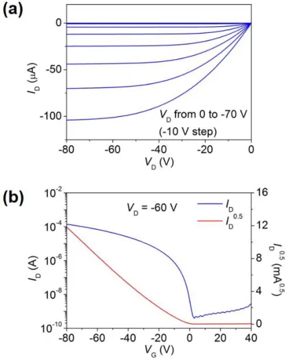
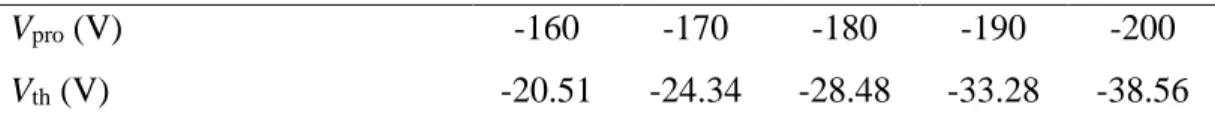
The second achievement is a write-once-read-many memory OFET using poly (vinyl cinnamate) as the charge trapping layer (Chapter 3). This memory OFETs exhibited Vth shifts of approximately 9, 18, 28 V after the programming voltages of - 160, -180 and -200 V, respectively. Although the programming voltages were high, this memory showed a high stability of logic states with a long retention time. In the later of the chapter 3, the proposed operation mechanism was discussed.
Chapter 4 introduces the main part of this dissertation, where a multi-level memory OFET was fabricated using Lithium-ion-encapsulated fullerene (Li+@C60) as a charge trapping material. The memory OFETs with a structure of
- 16 -
Si++/SiO2/Li+@C60/Cytop/Pentacene/Cu exhibited a performance of the p-type transistor with a Vth of -5.98 V and a μ of 0.84 cm2 V-1 s-1. The multi-level memory OFETs exhibited the ΔVth of approximate 10 V, 16 V, and 32 V, with a programming gate voltage of 150 V for 0.5 s, 5 s, and 50 s, and an erasing gate voltage of -150 V for 0.17 s, 1.7 s, and 17 s, respectively. Four logic states were clearly distinguishable in our multi-level memory, and its data could be programmed or erased many times.
The mechanism operation of the memory OFETs using Li+@C60 was discussed in detail. The memory effect of the OFETs is caused by the electrons
Fig.1.7. Structure of the dissertation
- 17 -
trapping at the Li+@C60. When the OFET was programmed for a short duration, the average number of trapped electrons per each Li+@C60 molecule was estimated based on the total of trapped electrons in the Li+@C60 layer over the density of Li+@C60
molecules per area. By programming for 0.5 s, the average number of trapped electrons per Li+@C60 molecule was 2.40 × 10⁻². Based on this result, we assumed that only Li+@C60 molecules at the surface of Li+@C60 domains could trap the electron. Beside the memory effect caused by the electron trapping, the Li+@C60
molecules were proposed to migrate into the pentacene layer. This migration causes the change in the ID of the OFET, which is one origin of the memory effect in our memory device. To confirm the charge trapping in the Li+@C60 molecules by electric field, an ultraviolet-visible spectroscopy (UV-Vis) measurement was carried out to detect an evidence. This work is reported in the chapter 5.
- 18 -
Reference
1. Ashok K. Sharma, Advanced semiconductor memories: architectures, design, and applications, Wiley-IEEE Press (2002)
2. S.M. Sze, Kwok K. Ng, Physics of semiconductor devices, 3rd edition, John Wiley & Sons (2006)
3. Joe Brewer, Manzur Gill, Nonvolatile memory technologies with emphasis on flash: a comprehensive guide to understanding and using flash memory devices, Wiley-IEEE Press (2007)
4. Chih-Tang Sah, Fundamentals of solid-state electronics, 1st edition, World Scientific (1991)
5. S. Mӧller, C. Perlov, W. Jackson, C. Taussig, S. R. Forrest, Nature 426, 166- 169 (2003)
6. F. Masuoka, M. Assano, H. Iwahashi, T. Komuro, and S. Tanaka, IEEE IEDM Tech. Dig., 88, 464-467 (1984)
7. https://en.wikipedia.org/wiki/EEPROM
8. https://en.wikipedia.org/wiki/Ferroelectric_RAM
9. N. Setter, D. Damjanovic, L. Eng, G. Fox, S. Gevorgian, S. Hong, A. Kingon, H. Kohlstedt, N.Y. Park, G.B. Stepenson, I. Stolitchnov, A.K. Taganstev, D.V.
Taylor, T. Yamada, S.Streiffer, J. Appl. Phys, 100, 051606 (2006) 10. R. Weiss, Electron. Des. 49, 56-64 (2001)
11. K.H. Lee, G. Lee, K. Lee, M.S. Oh, and S. Im, Appl. Phys. Lett. 94, 093304 (2009)
12. A.F. Devonshire, Theory of ferroelectrics: Advances in physics, 3, 85-130 (1954)
13. H. Ishiwara, M. Okuyama, Y. Arimoto, Ferroelectric random access memories, Berlin: Springer-Verlag (2004)
14. FRAM guide book. In: Fujitsu semiconductor memory manual, 5th edition.
Japan: Fujitsu Limited, 1-57 (2005)
15. B. Prince, Emerging memories: technologies and trends, Boston USA: Kluwer Academic Publishers (2002)
16. P. Heremans, G.H. Gelinck, R. Müller, K.-J. Baeg, D.-Y. Kim, and Y.-Y. Noh, Chem. Mater. 23, 341-358 (2011)
- 19 -
17. B. Cho, S. Song, Y. Ji, T.-W. Kim and T. Lee, Adv. Funct. Mater. 21, 2806- 2829 (2011)
18. Y. Sakuragawa, Y. Takagi, T. Ikai, K. Maeda, T.T. Dao, H. Sakai, and H.
Murata, Jpn. J. Appl. Phys. 55, 03DC10 (2016)
19. P. Stadler, K. Oppelt, T.B. Singh, J.G. Grote, R. Schwӧdiawer, S. Bauer, H.
Piglmayer-Brezina, D. Bäuerle, N. S. Sariciftci, Org. Electron. 8, 648-654 (2007)
20. R. Waser, R. Dittmann, G. Staikov, and K. Szot, Adv. Mater. 21, 2632-2663 (2009)
21. M. Wuttig, N. Yamada, Nat. Mater. 6, 824-832 (2007) 22. F. Jedema, Nat. Mater. 6, 90-91 (2007)
23. J.G. Simmons, R.R. Verderber, Pro. R. Soc. London Ser. A, 301, 77 (1967) 24. J. Ouyang, C.-W. Chu, C.R. Szmada, L. Ma, Y. Yang, Nat. Mater. 3, 918-922
(2004)
25. L.D. Bozano, B.W. Kean, M. Beinhoff, K.R. Carter, P.M. Rice, and J.C. Scott, Adv. Funct. Mater. 15, 1933-1939 (2005)
26. W. Guan, S. Long, M. Liu, Z. Le, Y. Hu, Q. Liu, J. Phys. D, 40, 2754-2758 (2007)
27. D.S. Kim, Y.H. Kim, C.E. Lee, Y.T. Kim, Phys. Rev. B, 74, 174430 (2006) 28. G.I. Meijer, U. Staub, M. Janousch, S.L. Johnson, B. Delley, T. Neisius, Phys.
Rev. B, 72, 155102 (2005)
29. A. Asamitsu, Y. Tomioka, H. Kuwahara, Y. Tokura, Nature 288, 50-52 (1997) 30. M.N. Kozicki, M. Yun, L. Hilt, A. Singh, J. Electrochem. Soc. 146, 298-309
(1999)
31. F.A. Krӧger, H.J. Vink, J. Phys. Chem. Solids, 5, 208-223 (1958)
32. I.M. Ross, Semiconductive translating devices, US patent: 2791760 (1957) 33. R.C.G. Naber, Ferroelectricity-functionalized organic field-effect transistors.
PhD thesis. Nijenborgh, The Netherlands: University of Groningen (2006) 34. R.C.G. Naber, C. Tanase, P.W.M. Blom, G.H. Gelinck, A.W. Marsman, F.J.
Touwslager, S. Setayesh, and D.M. de Leeuw, Nat. Mater. 4, 243-248 (2005) 35. R.C.G. Naber, B. de Boer, P.W.M. Blom, and D.M. de Leeuw, Appl. Phys.
Lett. 87, 203509 (2005)
36. D. Kahng, S.M. Sze, Bell Sys. Tech. J. 46, 1288-1295 (1967)
- 20 -
37. T. Sekitani, T. Yokota, U. Zschieschang, H. Klauk, S. Bauer, K. Takeuchi, M.
Takamiya, T. Sakurai, T. Someya, Science, 326, 1516-1519 (2009)
38. T. Yokota, T. Nakagawa, T. Sekitani, Y. Noguchi, K. Fukuda, U.
Zschieschang, H. Klauk, K. Takeuchi, M. Takamiya, T. Sakurai, and T.
Someya, Appl. Phys. Lett. 98, 193302 (2011)
39. S. Kolliopoulou, P. Dimitrakis, P. Normand, H.-L. Zhang, N. Cant, S.D. Evans, S. Paul, C. Pearson, A. Molloy, M.C. Petty, D. Tsoikalas, J. Appl. Phys. 94, 5234-5239 (2003)
40. Z. Liu, F. Xue, Y. Su, Y.M. Lvov, and K. Varahramyan, IEEE Trans.
Nanotechnol. 5, 379-384 (2006)
41. S.-J. Kim and J.-S. Lee, Nano Lett. 10, 2884-2890 (2010)
42. K.-J. Baeg, Y.-Y. Noh, H. Sirringhaus, D.-Y. Kim, Adv. Funct. Matter. 20, 224-230 (2010)
43. H.E. Katz, X.M. Hong, A. Dodabalapur, and R. Sarpeshkar, J. Appl. Phys, 91, 1572-1576 (2002)
44. K.-J. Baeg, Y.-Y. Noh, J. Ghim, S.-J. Kang, H. Lee, D.-Y. Kim, Adv. Mater.
18, 3179-3183 (2006)
45. K.-J. Baeg, Y.-Y. Noh, J. Ghim, B. Lim, and D.-Y. Kim, Adv. Funct. Mater.
18, 3678-3685 (2008)
46. K.-J. Baeg, D. Khim, J. Kim, B.-D. Yang, M. Kang, S.-W. Jung, I.-K. You, and Y.-Y. Noh, Adv. Funct. Mater. 22, 2915-2926 (2012)
47. K. Konno, H. Sakai, T. Matsushima, H. Murata, Thin Solid Films, 518, 534- 536 (2009)
48. T.T. Dao, T. Matsushima, H. Murata, Org. Electron. 13, 2709-2715 (2012) 49. M. Debucquoy, M. Rockele, J. Genoe, G.H. Gelinck, P. Heremans, Org.
Electron. 10, 1252-1258 (2009)
50. IEEE 1620-2004. IEEE Standard Test Methods for the Characterization of Organic Transistors and Materials
51. IEEE 1005-1998. IEEE Standard Definitions and Characterization of Floating Gate Semiconductor Arrays.
52. Rino Michelroni, Luca Crippa, Alessia Marelle, Inside NAND Flash Memories, Springer Science and Business Media (2010)
- 21 -
53. S.K. Hwang, L.M. Lee, S. Kim, J.S. park, H.I. Park, C.W. Ahn, K.L.Lee, T.
Lee, and S.O. Kim, Nano Lett. 12, 2217-2221 (2012)
54. J. Lee, A.J.J.M. van Breemen, V. Khikhlovskyi, M. Kermerink, R.A.J. Janssen, and G.H. Gelinck, Sci. Rep. 6, 24407 (2016)
55. W.Y. Kim, H.C. Lee, Org. Electron. 19, 1-6 (2015)
56. V. Khikhlovskyi, A.V. Gorbunov, A.J.J.M. van Breemen, R.A.J. Janssen, G.H.
Gelinck, M. Kemerink, Org. Electron. 14, 3399-3405 (2013)
57. M.A. Khan, J.A. Caraveo-Frescas, H.N. Alshareef, Org. Electron. 16, 9-17 (2015)
58. K. Tripathi, A.J.J.M. van Breemen, J.Shen, Q. Gao, M.G. Ivan, K. Reimann, E.R. Meinders, and G.H. Gelinck, Adv. Mater. 23, 4146-4151 (2011)
59. Y. Guo. C.-A. Di, S. Ye, X. Sun, J. Zeng, Y. Wen, W. Wu, G. Yu and Y. Liu, Adv. Mater. 21, 1954-1959 (2009)
60. Y.-C. Chiu, C.-L. Liu, W.-Y. Lee, Y. Chen, T. Kakuchi, and W.-C. Chen, NPG Asia Mater. 5, e35 (2013)
61. Y. Zhang, C. Lang, J. Fan, L. Shi, Y. Yi, Q. Yu, F. Guo, J. Wang, L. Zhao, Org. Electron. 35, 53-58 (2016)
- 22 -
CHAPTER 2 || AN EFFECT OF BACKGROUND PRESSURE ON THE PERFORMANCE OF MEMORY OFETS FOR MLC DEVICES*
We demonstrated an effect of vacuum pressure on the mobility (µ) and the threshold voltage (Vth) of organic field effect transistor (OFETs) using copper as source/drain (S/D) electrodes. By deposited under the background pressure of 2.5 × 10⁻⁵ Torr, the µ of the OFETs is c.a. 2 times and 3 times c.a. greater than that of the OFETs with gold and copper electrodes fabricated under low pressure of 1.6 × 10⁻⁶ Torr, respectively. The reason for the increase of the µ could be due to the charge injection barrier reduction, which caused by a penetration of oxygen into pentacene layer during deposition at high pressure.
*C.M. Tran, T. Murakami, H. Sakai, and H. Murata, IEICE Trans. Electron.
E100-C, 2, 122-125 (2017)
- 23 - 2.1. Introduction
Owing to their advantages of low cost, low temperature processing, and mechanical flexibility, organic field effect transistors (OFETs) could be applied in many applications such as organic memories, pressure sensors1-3. For the wide use, an improvement of OFETs performance as well as an increase in reliability and stability are required4. The performance of OFETs is determined by device’s parameters such as the µ, the Vth and the on/off ratio as well as a low operation voltages. In particular, an improvement of µ and a reduction of Vth have been research targets. To obtain this, an approach is an application of high-k material as the gate insulator5. In the case of OFETs using pentacene as semiconductor, both inorganic and organic high-k material such as barium zirconate titanate (BZT, k = 17.3, µ = 0.32 cm2 V-1 s-1, Vth = -4 V), barium strontium titanate (BTS, k = 16)6, aluminum oxide (Al2O3, k = 9, µ = 0.2 cm2 V-1 s-1, Vth = -2 V)7, tantalum oxide (Ta2O5, k = 23, µ = 0.8 cm2 V-1 s-1, Vth = -0.3 V)8, and poly (4-vinylphenol) (PVP)9, or photocross-linkable PVP10 were used. In addition, some polymer-nanoparticle composite dielectrics were also used for low voltage organic transistors11. For example, Zirkl er al. reported an OFET using nanoparticles of zirconium oxide (ZrO2) combined with poly (α-methyl styrene) (PαMS) as gate dielectric layer with a µ of 1.2 cm2 V-1 s-1 and a Vth of -1.1 V12. Moreover, a modification of the dielectric layer could be used to enhance a semiconductor film growth and reduce a leakage current in the OFET.
Another approach to increase the µ and to reduce the Vth of OFETs is by a reduction of a contact resistance between the S/D electrodes and semiconductor layer13. As charges are injected from the S/D electrodes, the reduction in contact resistance would increase the ID at low bias voltage applied to the gate (VG), resulting in better µ and Vth of OFETs. To reduce the contact resistance, the charge injection barrier between Fermi level energy of electrodes metal and lowest unoccupied molecular orbital (LUMO) level energy (for electron injection) or highest occupied molecular orbital (HOMO) level energy (for hole injection) needs to be decrease. To obtain this target, a very thin layer of metal oxide such as Ta2O514, molybdenum trioxide (MoO3)15, Al2O316, or cupric oxide (CuO)17 was inserted between S/D electrodes and the semiconductor layer. W. Gu et al. reported the use of a layer of copper sulfide (CuxS) instead of metal oxide. These OFETs using CuxS/Cu electrodes
- 24 -
obtained the µ of 2.3 cm2 V-1 s-1 and the Vth of -13 V as well. In this OFETs, Cu2+ and SO42- were considered to be responsible for the reduction of contact resistance18. This result shows us the application of Cu as S/D electrodes has much potential to improve the µ of the OFETs.
In this chapter, we present an effect of background pressure during electrode deposition on its contact resistance reduction, which results in the increase of the performance of the OFETs. The OFETs with copper electrodes deposited at a pressure of 2.5 × 10⁻⁵ Torr were found to show an increase in µ as well as a reduction of Vth
compared with those of copper and gold electrodes fabricated under lower background pressure.
- 25 - 2.2. Experimental
Figure 2.1 (a) and (b) show the cross structure and the illustration fabrication process of the OFETs in this work. The OFETs were fabricated on heavily doped silicon wafer (n+Si, resistivity of 1-10 Ω·cm) coasted with a 50-nm silicon dioxide (SiO2). These wafers were cleaned ultrasonically in acetone for 10 min, in pure water twice for 5 min each, and isopropyl alcohol (IPA) for 10 min, subsequently subjected
Fig.2.1. (a) A cross structure, and (b) an illustration fabrication process of OFETs
- 26 -
to an ultraviolet-ozone surface treatment (UV-O3) for 30 min. All substrates in this dissertation were cleaned follows this cleaning process.
The SiO2 surface was modified by a thin layer of Cytop (CTL-809 M, Asahi Glass). This layer was fabricated by spin-coating at 2,500 rpm for 60 seconds using a solution with a concentration of 0.5 wt%, followed by drying at 100 ºC for 2 h. The thickness of the Cytop layer was ~10 nm, measured by an atomic force microscopy (AFM, Keyence VN-8000 nanoscale hybrid microscopy).
For an active layer of OFETs, a layer of pentacene was thermally deposited under a background pressure of 1.6 × 10⁻⁶ Torr and a deposition rate of 0.3 Å/s. The copper S/D electrodes were sequentially deposited by using shadow masks at a higher pressure of 2.5 × 10⁻⁵ Torr and a deposition rate of 0.3 Å/s. The length (L) and width (W) of the channel were 50 µm and 2,000 µm, respectively. The thickness of Cu electrodes was 50 nm.
For comparison, OFETs using gold and Cu electrodes deposited under 1.6 × 10⁻⁶ Torr were fabricated.
The electrical characteristics of the OFETs were measured with a Keithley 4200 semiconductor characterization system in a dry nitrogen atmosphere at room temperature.
- 27 - 2.3. Basic parameters of OFETs
2.3.1. Electrical characteristics configuration
In order to determine the characteristics of OFETs, a Keithley 4200 semiconductor characterization system (SCS 4200) was used in this dissertation. The SCS 4200 consists of pre-appliers (PreAmps), current/voltage sources, ampere/voltage meters and oscilloscopes, which are integrated in a computer. For a basic characterization of OFETs such as transfer, output measurements, the SCS 4200 operated in a sweeping mode. Fig. 2.2 shows a setup for a basically electrical measurement of OFETs.
2.3.2. Electrical characteristics of OFETs
Figure 2.3 (a) shows a tantamount electric circuit which is used for output characteristics measurement. The ID of OFET were measured while the S-D voltage (VD) was varied from 0 to -10 V at different VG sweeping from 0 to -10 V with a step of -2 V. As shown in Fig. 2.3 (b)-(d), the ID of all transistors increased linearly at low VD, and became saturated at high VD, because the conducting channel in the pentacene layer was pinched off. All the devices exhibited the characteristics as typical p- channel OFETs. At the same VD of -10 V and VG of -10 V, the on-state current (-8.97 µA) of OFETs with Cu electrodes deposited at high pressure is c.a. 10 times greater than that of the OFET using gold electrodes (-0.88 µA). Within the comparison of Cu electrodes devices, high pressure brings about c.a. 64 times greater current than that of low pressure devices (-0.14 µA) (Fig. 2.3. (b)-(d)).
Fig.2.2. Setup for characterization of OFETs
- 28 -
Fig.2.3. (a) Tantamount circuit for output characteristics, the output curves of OFET with (b) Cu electrodes deposited under a pressure of 2.5 × 10⁻⁵ Torr, with (c) gold and Cu (d) electrodes deposited under pressure of 1.6 × 10⁻⁶ Torr.
- 29 -
Fig.2.4. (a) Tantamount circuit for transfer characteristics, the transfer curves of OFET with (b) Cu electrodes deposited under a pressure of 2.5 × 10⁻⁵ Torr, with (c) gold and Cu (d) electrodes deposited under pressure of 1.6 × 10⁻⁶ Torr.
- 30 -
For a transfer characteristics measurement, a voltage sweeping from 2 to -10 V was applied to the gate with a step of -0.5 V while a voltage applied to the D electrode was kept at -10 V (Fig. 2.4. (a)). The µ of devices were calculated from the saturated regime, using the conventional metal-oxide- semiconductor equation19:
𝐼𝐷,𝑠𝑎𝑡= 𝑊𝐶𝑖
2𝐿 µ(𝑉𝐺 − 𝑉𝑡ℎ)2
where ID,sat is the saturated drain current, W and L are the length and width of the channel. Ci is the capacitance per unit area of the gate dielectric. In our OFETs, the gate capacitor could be considered as the Cytop capacitor in serial connection with the SiO2 capacitor. Thus, Ci could be estimated to be 8.25 nF/cm2 from their thickness and the permittivity of Cytop and SiO2. The electrical characteristics of all transistors were calculated and summarized in the table 2.1. The Cu electrode OFET fabricated under high pressure has the best electrical characteristics with the µ of 0.13 cm2 V-1 s-
1, the Vth of -2.56 V and an on/off ratio of 8.13 × 10⁴. The µ of this OFET is c.a. 2 times and c.a. 3 times greater than that of the OFETs with gold and Cu electrodes fabricated under low pressure, respectively. Moreover, the reduction in Vth of 0.75 V and 5.54 V is also observed. Thus, it is clear that the OFETs with Cu electrodes fabricated under high pressure have the best performance.
Table 2.1. OFETs parameters Metal for
electrodes
Background pressure for S/D deposition (Torr)
µ (cm2 V-1 s-1)
Vth
(V)
On/off ratio
Copper 2.5 × 10⁻⁵ 0.13 -2.56 8.13 × 10⁴
Gold 1.6 × 10⁻⁶ 0.05 -3.31 3.76 × 10⁵
Copper 1.6 × 10⁻⁶ 0.04 -8.10 6.05 × 10³
- 31 -
2.4. Effect of background pressure on a contact resistance reduction
In the previous section, the effect of background pressure on the performance of OFETs was observed. The OFETs with Cu electrodes fabricated under high background pressure of 2.5 × 10⁻⁵ Torr exhibited the highest µ and the lowest Vth
compared with those of OFETs with gold and Cu electrodes fabricated under low background pressure of 1.6 × 10⁻⁶ Torr. Because all the OFETs had the same fabrication process, an enhance of the OFET performance is not caused by the modification of the dielectric layer. We supposed that the change in the contact resistance (RC) is the origin of this effect.
In order to examine the RC of OFETs, the transmission line method (TLM) is normally used20,21. By this method, a relationship between the length of channel (L) and the total resistance (RT) was determined from some the RC of OFETs with the different L. Based on this relationship, the RC was estimated to be RT/2 corresponding to an extreme small of L. However, in our study, TLM method could not be used due to the fixed geometry of L in our devices.
Here we assume that a resistance of the channel (Rch) would have an identical value, because all transistors were fabricated under the same architecture with the same L, W and the same thickness of pentacene layer. Thus, the change in RT will corresponds to the change in the RC18. Fig. 2.5 shows the total resistances of the OFETs. As can be seen, the resistance of the OFETs with Cu electrodes fabricated under high pressure showed the lowest resistance. This suggest that these OFETs would have the lowest charge injection barrier, which caused the higher µ than that of other OFETs.
Fig.2.5. Total resistance of OFETs channel as a function of gate voltage
- 32 -
2.5. An origin of the reduction of contact resistance
2.5.1. The contact resistance reduction due to an existence of CuO between the pentacene layer and Cu electrodes
To deeply understand the reduction of contact resistance of OFETs, an X-ray photoelectron microscopy (XPS) was carried out to investigated an existence of CuO.
In the case of Cu deposited at high background pressure, we assume that a few Cu atoms could oxidize with oxygen which remained in the chamber of the evaporation machine. These molecules of CuO would exist between the pentacene layer and Cu electrodes, resulting in the reduction of contact resistance of OFETs, which was reported in the literature17.
The depth profile measurement of XPS for S/D electrodes and pentacene were performed, where a beam of Ar+ ions was used to dig from the electrodes, followed by the XPS measurement. This procedure was repeated until signals of both C and Cu were obtained at the same time, which corresponds to the spectra at the interface between Cu electrodes and the pentacene layer. Fig. 2.6 shows the XPS spectra at the interface. In Fig 2.6. (a), there is no obvious shift in C 1s peak so that there is no chemical reaction of pentacene at the interface. Thus, the enhancement of µ of the OFETs using Cu electrodes does not come from a chemical reaction between Cu and pentacene. On the other hand, Fig 2.6. (b) and (c) do not show the existence of both Cu2+ ions and oxygen which are presented by peaks in XPS spectra at a binding energy of 963.3, 942.4, 944.6 and 530.0 eV 22. Thus, the existence of CuO could not be observed at the interface. In this case, I assume that this might be due to the weak signal to detect.
2.5.2. The contact resistance reduction due to a penetration of oxygen into the pentacene
Another possibility for the contact resistance reduction is a penetration of oxygen into the pentacene layer during deposition, which was reported by Vollmer et al. in 200523. It was reported that oxygen exposure lowers the hole injection barrier at the interface between gold and pentacene. At high pressure, oxygen which remained in the chamber might penetrate into the pentacene layer. This may cause a reduction
- 33 -
of hole injection barrier, which is similar to that of gold/pentacene interface. This could cause the reduction of contact resistance in OFETs, and correspond to the high in the µ.
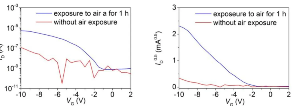
To clarify an effect on oxygen on the µ of the OFETs, other OFETs were fabricated, which were exposed to ambient air for 1 h before electrodes fabrication at
Fig.2.6. X-ray photoelectron spectroscopy. The C 1s spectrum (a), Cu 2p spectrum (b), and O 1s spectrum (c) at pentacene/Cu interface of samples, which fabricated at 2.5 × 10⁻⁵ Torr and 1.6 × 10⁻⁶ Torr.
- 34 -
a low pressure of 1.6 × 10⁻⁶ Torr. As shown in Fig. 2.7, the OFET with air exposure before S/D Cu electrodes fabrication shows the better performance than that of the devices without air exposure. The electrical characteristics of these OFETs were calculated and summarized in the table 2.2. Based on this result, the effect of oxygen on the µ of OFETs was confirmed. Thus, we conclude that the reduction of contact resistance of OFETs could be due to the penetration of oxygen into the pentacene layer, which corresponds to the high µ in our OFETs
Table 2.2. Parameters of OFETs with copper electrodes deposited at a pressure of 1.6 × 10⁻⁶ Torr.
OFETs µ
(cm2 V-1 s-1)
Vth
(V)
On/off ratio With air exposure for 1 h 0.13 -3.24 7.19 × 10³
Without air exposure 0.04 -8.10 6.05 × 10³
Fig.2.7. The transfer curves of the OFETs with Cu electrodes deposited at a pressure of 1.6 × 10⁻⁶ Torr (VD = -10 V).
- 35 - 2.6. Conclusions
In summary, we reported the effect of deposition pressure on the performance of OFETs using copper as source/drain electrodes. These OFETs with copper electrodes fabricated at high pressure exhibit better performance compared with conventional gold- or copper-based devices. The reason for the µ enhancement of our OFETs could be due to the charge injection barrier reduction, which caused by the penetration of oxygen into pentacene layer during deposition under high pressure. A mechanism of background pressure effects on the performance of OFETs using copper electrodes has not been clearly understood yet. However, we believe this result would be helpful for improving OFETs performance using a simple method which could be applied in industrial applications.
- 36 - Reference
1. M.L. Hammock, A. Chortos, B.C.-K. Tee, J.B.-H. Tok, and Z. Bao, Adv.
Mater. 25, 5997-6038 (2013)
2. M. Kaltenbrinner, T. Sekitani, J. Reeder, T. Yokota, K. Kuribara, T. Tokuhara, M. Drack, R. Schwӧdiauer, I. Graz, Bauer-Gogorea, S. Bauer, and T. Someya, Nat. Lett. 499, 458-463 (2013)
3. Y. Tsuji, H. Sakai, L. Feng, X. Guo, and H. Murata, Appl. Phys. Express 10, 021601 (2017)
4. T. Sekitani, and T. Someya, Jpn. J. Appl. Phys. 51, 100001 (2012)
5. R.P Ortiz, A. Facchetti, and T.J. Marks, Chem. Rev. 110, 205-239 (2010) 6. C.D. Dimitrakopoulos, S. Purushothaman, J. Kymissis, A. Callegari, and J.M.
Shaw, Science 283, 822-824 (1999)
7. S. Goettling, B. Diehm, and N. Fruehauf, J: Disp. Technol. 4, 300-303 (2008) 8. H. Sakai, Y. Furukawa, E. Fujiwara, and H. Tada, Chem. Lett. 33, 1172-1173
(2004)
9. M. Halik, H. Klauk, U. Zschieschang, T. Kriem, G. Schmid, W. Radlik, and K. Wussow, Appl. Phys. Lett. 81, 289-291 (2002)
10. S.C. Lim, S.H. Kim, J.H. Lee, H.Y. Yu, Y. Park, D. Kim and T. Zyung, Mater.
Sci. Eng. B, 121, 211-215 (2005)
11. R. Schroeder, L.A. Majewski, and M. Grell, Adv. Mater. 17, 1535-1539 (2005)
12. M. Zirkl, A. Hasse, A. Fian, H. Schӧn, C. Sommer, G. Jakopic, G. Leising, B.
Stadlober, I. Graz, N. Gaar, R. Schwӧdiauer, S. Bauer-Gogonea, and S. Bauer, Adv. Mater. 19, 2241-2245 (2007)
13. C. Liu, Y.Xu, and Y.-Y. Noh, Material Today 18, 79-96 (2015)
14. T. Maeda, H. Kato, and H. Kawakami, Appl. Phys. Lett. 89, 123508 (2006) 15. M. Kano, T. Minary, K. Tsukagoshi, Appl. Phys. Lett. 94, 143304 (2009) 16. P. Darmawan, T. Minari, A. Kumatami, Y. Li, C. Liu, and K. Tsukagoshi,
Appl. Phys. Lett. 100, 013303 (2012)
17. W. Hu. K. Manabe, T. Furukawa, and M. Matsumura, Appl. Phys. Lett. 80, 2640-2641 (2002)
18. W. Gu, W. Jin, B. Wei, J. Zhang, and J. Wang, Appl. Phys. Lett. 97, 243303 (2010)
- 37 -
19. I. Kymissis, Organic Field Effect Transistors: Theory, Fabrication and Characterization, Springer (2009)
20. http://tuttle.merc.iastate.edu/ee432/topics/metals/tlm_measurements.pdf 21. M. Weis, K. Lee, D. Taguchi, T. Manaka, and M. Iwamoto, Jpn. J. Appl. Phys.
53, 011601 (2014)
22. S. Poulson, P.M. Parlett, P. Stone, and M. Bowker, Surface and Interface analysis 24, 811-820 (1996)
23. A. Vollmer, O.D. Jurchescu, I. Arfaoui, I. Salzmann, T.T.M. Palstra, P. Rudolf, J. Niemax, J. Pflaum, and N. Koch, Eur. Phys. J. E. 17, 339-343 (2005)
- 38 -
CHAPTER 3 || WRITE-ONCE-READ-MANY MLC MEMORY OFETS USING POLY (VINYL CINAMMATE) AS CHARGE TRAPPING LAYER*
A thin layer of poly (vinyl cinnamate) (PVCN) was used as a charge trapping layer in a pentacene OFET. The memory characteristics of the devices showed a non- volatile write-once-read-many memory behavior with the shifts of the threshold voltage of approximately 9, 17, 27 V after applying the programming voltages of - 160, -180, and -200 V for 3 seconds, respectively. The memory OFETs with an on/off ratio of 105 exhibited stable logic states with retention time of 11,000 seconds. The memory effect in this OFET is ascribed to trapped holes at the interface between PVCN and silicon dioxide (SiO2) layer. An ultraviolet photoelectron spectroscopy (UPS) and an ultraviolet-visible spectroscopy (UV-Vis) measurements were carried out to estimate the highest occupied molecular orbital (HOMO) and the lowest unoccupied molecular orbital (LUMO) of PVCN. Based on this result, the operation mechanism was proposed.
*C.M. Tran, H. Sakai, T. Murakami, and H. Murata, (Under preparation)
- 39 - 3.1. Introduction
In previous chapters, both the advantages and the disadvantages of organic MLC memories were discussed. Although resistor-1,2 and capacitor-based3,4 MLC memories exhibited a low operation voltage, the use of these memories required external circuit of a diode5, or a transistor6,7. These structures may require a high-cost and complicated fabrication with 2 components in each cell. Thus, the transistor-based MLC memory OFETs have been attracted attention even if they operate at high voltage. From this point of this dissertation, I would like to focus on this structure of MLC devices.
In a charge trapping memory OFET, a thin film layer of polymer such as PαMS8,9, PS10, PVA10,11, PMMA12, Cytop13 was inserted between dielectric layer and an active layer. Under an applied electric field, charges are injected from the S/D electrodes and trapped. The trapped charges would induce a change in the ID or a shift of the Vth of memory OFETs, which still remain after electric field removal. This causes the memory effect in the OFETs.
A MLC memory effect in the OFETs is presented by several ON states of OFETs, which are obtained by applying different voltages. Guo et al. reported MLC memory OFETs based on a semiconductor of pentacene or copper phthalocyaine (CuPc)14. For the charge trapping layer, PS or PMMA could be used. The OFET using a trapping layer of PS showed a p-type behavior with the µ of 0.52 cm2 V-1 s-1, the Vth
of -20 V and the on/off ratio of 106. In this memory, 7 level of ON states could be obtained. However, the programming/erasing operation required an assisted light source for the reduction of programming/erasing voltages. This requirement caused a limitation for its usage. In 2013, Chiu et al. reported write-once-read-many MLC memory OFET using a n-type semiconductor of N,N’-bis(2-phenylethyl)perylene- 3,4,9,10-bis (dicarbonximide) and the charge trapping layer of a star-shaped poly((4- diphenylamino) benzyl methacrylate (star-PTPMA)15. However, the programming voltage up to 200 V was used to operate this memory. Recently, another MLC memory OFETs with the charge trapping structure was reported by Zang et al. in 201616. This device used the new material of polyquinoline (PQ) to trap electrons in a pentacene transistor. These trapped electrons caused a hysteresis in the transfer curve, which corresponded to the MLC effect. The programming voltage in this memory was