A Novel Reduction Strategy of Standby Power Loss in the Multi-Oscillated Current Resonant DC-DC Converter
Considering Acoustic Noise Compatibility
1) Fuji Electric Co., Ltd.
2) Graduate School of Science and Technology, Nagasaki University E-mail: [email protected]
Abstract— The current resonant type DC-DC converter employs generally the pulse frequency modulation and its magnetizing inductance is set relatively low. For this reason, the magnetizing current through the converter causes a power loss under the light load condition. To solve this problem, a multi-oscillated current resonant type DC-DC converter has been proposed and then the advantage of its control method has been clarified, which can reduce power loss under light load condition and keep low switching noise. This paper deals with a novel reduction strategy of standby power consumption of the converter. As a result, the standby power consumption under no load condition is achieved below 60mW at 100V AC input and 150mW at 240V AC input, respectively. Furthermore, it is clarified that the slope of the re- sonant current envelope at soft start and end function in the standby mode influence the acoustic noise from the converter.
Keywords; resonant converter, standby-power consumption, acoustic noise I. I NTRODUCTION
The current resonant type DC-DC converter, which has ad- vantage of high efficiency, low noise and small size, is used widely in consumer electronics, telecommunication systems and so forth [1-12]. The pulse frequency modulation (PFM) is employed generally in this type of converter [1-12]. However, this type of converter has deteriorated problems, in which a magnetizing current through the converter causes a loss of power under the light load condition. Also, it is difficult to re- duce power consumption under no load condition i.e. in the standby mode. So, it is necessary to use another isolated con- verter which is relatively large in order to reduce the standby mode power loss.
To solve these problems, a multi-oscillated current reso- nant DC-DC converter has been proposed [13-18]. It has been clarified in recent some papers that the high power efficiency (maximum one over 96% in DC-DC section) is achieved under the condition from the light load by using the PWM and self- oscillation [17, 18].
This type converter has adopted the intermittently switch- ing mode in the standby mode [15]. In generally, the function of intermittently switching is able to reduce power consump- tion, but it has a problem with the acoustic noise compatibility.
This paper presents a novel standby control strategy for the multi-oscillated current resonant DC-DC converter, which is superior to the former paper. Furthermore, the reduction of the power consumption in the standby mode is discussed with con- sidering the acoustic noise compatibility.
II. C IRCUIT C ONFIGRATION
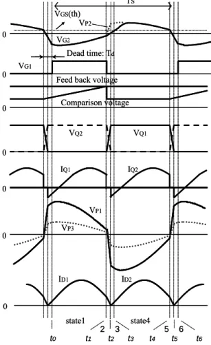
Figure 1 and 2 show the proposed multi-oscillated current resonant DC-DC converter and the timing chart, respectively.
This converter consists of a half-bridge circuit, whose switches Q
1and Q
2which consist of MOSFET, are operated by a multi- oscillated current resonant driven by an IC with pulse-width modulation (PWM), and an auxiliary winding N
P2of the trans- former, respectively.
In this converter, a multi-chip power module which consists of a control IC and two MOSFETs into one package is adopted.
Furthermore, a startup circuit which is connected to the input voltage of this converter is included in the control IC of this module. Therefore, PWB pattern is minimized than they are composed as all discrete devices.
In the Fig. 1, an AC input is converted to DC voltage through the AC-DC rectifier bridge and PFC circuit which is normally used a PFC control IC in former step of this converter.
The leakage inductance of transformer is included in T
r(It is omitted in the figure). In the secondary side, a sub DC-DC converter is added for supplying the voltage to the system con- trol (e.g. CPU and its peripheral). This sub DC-DC converter is also used in the standby mode. It is important to note that the isolation element is unnecessary such as AC-DC converter, in which its size is very small and the circuit configuration is very simple.
Tadahiko SATO
1, 2, Hirofumi MATSUO
2and Hiroyuki OTA
1Self-oscillation circuit
IC
Power IC (Fuji M-Power2)
Q1
Rectification and PFC circuit
Q2
VP1
VQ1
VQ2
IQ2
IQ1 VG2
VG1
ID1
ID2
VO
Normal / Stand-by signal from system control Ed
PWM control
Cr
Tr
Feedback circuit
NP1
NS1
NS2
NP2
NP3
Co
NP4 Vin(ac)
DC-DC Converter VOsub
Startup circuit
VCr
VP2
VP3
CVCC
Opt-coupler Opt-coupler ICC
VCC
Self-oscillation circuit
IC
Power IC (Fuji M-Power2)
Q1
Rectification and PFC circuit
Q2
VP1
VQ1
VQ2
IQ2
IQ1 VG2
VG1
ID1
ID2
VO
Normal / Stand-by signal from system control Ed
PWM control
Cr
Tr
Feedback circuit
NP1
NS1
NS2
NP2
NP3
Co
NP4 Vin(ac)
DC-DC Converter VOsub
Startup circuit
VCr
VP2
VP3
CVCC
Opt-coupler Opt-coupler ICC
VCC
Fig. 1 Circuit configuration
By applying a gate voltage to Q
1and Q
2at turn-on and turn-off, switching power losses are reduced due to the zero- voltage switching (ZVS) and zero-current switching (ZCS).
In the isolated transformer T
r, the primary winding N
P1is loosely coupled to the secondary windings N
S1and N
S2, for in which the voltage of the leakage inductance is relatively large.
Because of the resonant circuit with this leakage inductance and the resonant capacitor, the switching power losses of Q
1and Q
2are reduced.
A winding of transformer N
P3is added for timing detection of Q
1. The polarity of this winding is opposite to N
P2, which is used to drive Q
2. Moreover, the control IC turns Q
1off before N
P3turns to negative. Therefore this converter prevents arm short automatically.
In this converter, to realize the novel standby operation, the winding N
P4for the power supply V
CCis coupled strongly to the secondary windings and it is electrically isolated from the secondary side. And the control IC detects the output voltage V
Oindirectly by observing V
CCin the standby mode.
In the normal operation, the input voltage for this converter is regulated to 400 V DC by PFC circuit. On the other hand, in the standby mode, the input voltage for this converter is varied from about 140 to 340 V DC in universal input because a pow- er supply to the PFC circuit is turned off for reducing power consumption.
III. O PERATION P RINCIPLE
A. Basically Operating mode (Normal Mode)
Figure 3 shows the equivalent circuits of the converter shown in Fig. 1, which is divided into eight behavior states. Taking into account the combination of the eight states of behavior, they are further divided into four operating modes [16].
Figure 4 shows the simulated waveforms of the current and voltage for the four operating modes. From the results, the op-
V
Q1V
Q20
I
Q2I
Q10
V
P10
I
D1I
D20 0
Dead time: T
d0
0
Feed back voltage Comparison voltage V
GS(th)
V
P2V
G2V
P3state1 3 2
state4 5 6
t
0t
1t
2t
3t
4t
5t
6T
SV
G1V
Q1V
Q20
I
Q2I
Q10
V
P10
I
D1I
D20 0
Dead time: T
d0
0
Feed back voltage Comparison voltage V
GS(th)
V
P2V
G2V
P3state1 3 2
state4 5 6
t
0t
1t
2t
3t
4t
5t
6T
SV
G1Fig. 2 Timing chart
(a) state 1 Ed
D1
D2
Q2
Q1
Cr Ll2
Co CQ2
CQ1
DQ2
DQ1
ILm Ll1
ILl
Lm
ID1
(b) state 2 DQ2
Ed
D1
D2
Q2
Q1
Cr Ll2
Co CQ2
CQ1
DQ1
ILm Ll1
ILl
Lm
ID1
Ed
D1
D2
Q2
Q1
Cr Ll2
Co CQ2
CQ1
DQ2
DQ1
ILm Ll1
ILl
Lm
(c) state 3 ID2
Ed
D1
D2
Q2
Q1
Cr Ll2
Co CQ2
CQ1
DQ2
DQ1
ILm Ll1
ILl
Lm
(d) state 4 ID2
(e) state 5 DQ2
Ed
D1
D2
Q2
Q1
Cr Ll2
Co CQ2
CQ1
DQ1
ILm Ll1
ILl Lm
ID2
Ed
D1
D2
Q2
Q1
Cr Ll2
Co CQ2
CQ1
DQ2
DQ1
ILm
Ll1
ILl Lm
(f) state 6 ID1
Ed
D1
D2
Q2
Q1
Cr Ll2
Co CQ2
CQ1
DQ2
DQ1
ILm Ll1
Lm
(g) state 7
D1
D2
Q2
Q1
Cr Ll2
Co CQ2
CQ1
DQ2
DQ1
ILm
Ll1
Lm
(h) state 8 (a) state 1
Ed
D1
D2
Q2
Q1
Cr Ll2
Co CQ2
CQ1
DQ2
DQ1
ILm Ll1
ILl
Lm
ID1
(a) state 1 Ed
D1
D2
Q2
Q1
Cr Ll2
Co CQ2
CQ1
DQ2
DQ1
ILm Ll1
ILl
Lm
ID1 D1
D2
Q2
Q1
Cr Ll2
Co CQ2
CQ1
DQ2
DQ1
ILm Ll1
ILl
Lm
ID1
(b) state 2 DQ2
Ed
D1
D2
Q2
Q1
Cr Ll2
Co CQ2
CQ1
DQ1
ILm Ll1
ILl
Lm
ID1
(b) state 2 DQ2
Ed
D1
D2
Q2
Q1
Cr Ll2
Co CQ2
CQ1
DQ1
ILm Ll1
ILl
Lm
ID1
DQ2
Ed
D1
D2
Q2
Q1
Cr Ll2
Co CQ2
CQ1
DQ1
ILm Ll1
ILl
Lm
ID1
Ed
D1
D2
Q2
Q1
Cr Ll2
Co CQ2
CQ1
DQ2
DQ1
ILm Ll1
ILl
Lm
(c) state 3 ID2
Ed
D1
D2
Q2
Q1
Cr Ll2
Co CQ2
CQ1
DQ2
DQ1
ILm Ll1
ILl
Lm
Ed
D1
D2
Q2
Q1
Cr Ll2
Co CQ2
CQ1
DQ2
DQ1
ILm Ll1
ILl
Lm
(c) state 3 ID2
Ed
D1
D2
Q2
Q1
Cr Ll2
Co CQ2
CQ1
DQ2
DQ1
ILm Ll1
ILl
Lm
(d) state 4 ID2
Ed
D1
D2
Q2
Q1
Cr Ll2
Co CQ2
CQ1
DQ2
DQ1
ILm Ll1
ILl
Lm
Ed
D1
D2
Q2
Q1
Cr Ll2
Co CQ2
CQ1
DQ2
DQ1
ILm Ll1
ILl
Lm
Ed
D1
D2
Q2
Q1
Cr Ll2
Co CQ2
CQ1
DQ2
DQ1
ILm Ll1
ILl
Lm
(d) state 4 ID2
(e) state 5 DQ2
Ed
D1
D2
Q2
Q1
Cr Ll2
Co CQ2
CQ1
DQ1
ILm Ll1
ILl Lm
ID2
(e) state 5 DQ2
Ed
D1
D2
Q2
Q1
Cr Ll2
Co CQ2
CQ1
DQ1
ILm Ll1
ILl Lm
ID2
DQ2
Ed
D1
D2
Q2
Q1
Cr Ll2
Co CQ2
CQ1
DQ1
ILm Ll1
ILl Lm
ID2
Ed
D1
D2
Q2
Q1
Cr Ll2
Co CQ2
CQ1
DQ2
DQ1
ILm
Ll1
ILl Lm
(f) state 6 ID1
Ed
D1
D2
Q2
Q1
Cr Ll2
Co CQ2
CQ1
DQ2
DQ1
ILm
Ll1
ILl Lm
Ed
D1
D2
Q2
Q1
Cr Ll2
Co CQ2
CQ1
DQ2
DQ1
ILm
Ll1
ILl Lm
Ed
D1
D2
Q2
Q1
Cr Ll2
Co CQ2
CQ1
DQ2
DQ1
ILm
Ll1
ILl Lm
(f) state 6 ID1
Ed
D1
D2
Q2
Q1
Cr Ll2
Co CQ2
CQ1
DQ2
DQ1
ILm Ll1
Lm
(g) state 7 Ed
D1
D2
Q2
Q1
Cr Ll2
Co CQ2
CQ1
DQ2
DQ1
ILm Ll1
Lm
(g) state 7
D1
D2
Q2
Q1
Cr Ll2
Co CQ2
CQ1
DQ2
DQ1
ILm
Ll1
Lm
(h) state 8 D1
D2
Q2
Q1
Cr Ll2
Co CQ2
CQ1
DQ2
DQ1
ILm
Ll1
Lm
(h) state 8
Fig. 3 Equivalent circuits and operation states
1 2 7 5 6
state
VQ1 ICr
VCr ID1
ID2
0 0 0 0
VQ2
(a) Mode I
1 2 7 5 6
state
VQ1 ICr
VCr ID1
ID2
0 0 0 0
VQ2
(a) Mode I
1 2 4 7 5 6
state 0 0 0 0
VQ1 VQ2
ICr
VCr ID1
ID2
(b) Mode II
1 2 4 7 5 6
state 0 0 0 0
VQ1 VQ2
ICr
VCr ID1
ID2
(b) Mode II
1 2 3 4 5 6
state 0 0 0 0
VQ1 VQ2
ICr
VCr
ID1 ID2
(c) Mode III
1 2 3 4 5 6
state 0 0 0 0
VQ1 VQ2
ICr
VCr
ID1 ID2
(c) Mode III
1 2 5 6
state 8 3 4
0 0 0 0
VQ1 VQ2
ICr
VCr
ID1 ID2
(d) Mode IV
1 2 5 6
state 8 3 4
0 0 0 0
VQ1 VQ2
ICr
VCr
ID1 ID2
(d) Mode IV
Fig. 4 Operation modes
erating modes appear in the order of I, II, III and IV when the load current is varied from the light load to the heavy load.
The operating modes I and II mainly appear at light load.
The energy in C
ris discharged when the Q
1turns off and Q
2turns on, and charged by applying the output voltage E
dof the PFC when the Q
1turns on and Q
2turn off. Therefore, the ener- gy is discharged to the secondary side through the transformer.
However, because of the magnetizing inductance L
mis set rela- tively large when there is shortage of the energy discharged from C
r, operating state 7 appears, in which there is no dis- charging interval to the secondary side.
In the mode III, a ripple is reduced and smoothed by the leakage inductance L
l2of the secondary winding and the output capacitor C
obecause the current flows continuously through D
1and D
2, alternately.
The Mode IV appears when the duty ratio is almost over 50 %. In this mode, the state 8 appear where the power is not applied to the secondary side even when Q
1turns on.
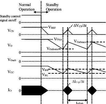
B. Standby Mode
Figure 5 shows block diagram of control circuit that is re- lated to standby function and figure 6 shows the on period of Q
1characteristic. In the standby mode, voltage V
CSof a capaci- tor C
CSdetermines the on period of Q
1.
Figure 7 shows the timing chart of standby mode. In the standby mode, the system control in the secondary side releases the pulled-up connection to the reference voltage of the control IC (approximately 5V). Then the control IC discharges C
CSwith constant current I
CS, so the on-period of Q
1is narrowed gradually as V
CSis decreasing, then stops switching in time (soft-end function).
When switching is stopped, supplying to the voltage of the control IC’s power supply V
CCis also stopped, and then this voltage is reduced gradually by the power consumption of IC.
And the output voltage V
Ois also reduced by the power con- sumption of the secondary side, but the output voltage V
Osubfor the system control of the secondary side is stabilized by the DC-DC converter in the secondary side.
If V
CCbecomes under the threshold voltage of V
BL, the con- trol IC starts charging C
CSby constant current I
CSand starts switching with the on period of Q
1limited by V
CS(soft-start function).
As the switching is restarted, V
CCand V
Oare increased.
When V
CCreaches the threshold voltage of V
BH, the control IC changes to soft-end function.
That is, this converter operates in intermittently switching with soft-start and soft-end function. The on period of Q
1and the peak of the resonant current increases and decrease gradual- ly. And the slope of the resonant current envelope I
Crp/t is able to be adjusted with C
CS.
Therefore, this function is expected to suppress acoustic noise because it is known that a drastic change of a current through the transformer causes an acoustic noise [15].
System control V
Oor V
OsubOpt-coupler Secondary side Primary side
C
CSV
CSV
REFI
CSI
CSTo PWM complator from reference voltage of IC
GND
from V
CClevel detector Control IC
CS
System control V
Oor V
OsubOpt-coupler
System control V
Oor V
OsubOpt-coupler Secondary side Primary side
C
CSV
CSV
REFI
CSI
CSTo PWM complator from reference voltage of IC
GND
from V
CClevel detector Control IC
CS
Primary side
C
CSV
CSV
REFI
CSI
CSTo PWM complator from reference voltage of IC
GND
from V
CClevel detector Control IC
CS C
CSV
CSV
REFI
CSI
CSTo PWM complator from reference voltage of IC
GND
from V
CClevel detector Control IC
CS
Fig. 5 Block diagram of control circuit (Related to standby function)
0 5 10 15 20 25 30
0 1 2 3 4 5
V
CS[V]
O n- p er iod of Q
1[µ s]
Fig. 6 On period of Q
1characteristic
V
CCI
CrV
OsubV
OV
CS Standby control signal on/offNormal Operation
Standby Operation
V
BHV
BLV
Otyp0 0 0 0 0 0
V
REFV
CS/t
I
Crp/t V
OstbmaxV
Ostbmint
offstbV
CCI
CrV
OsubV
OV
CS Standby control signal on/offNormal Operation
Standby Operation
V
BHV
BLV
Otyp0 0 0 0 0 0
V
REFV
CS/t
I
Crp/t V
OstbmaxV
Ostbmint
offstbFig. 7 Timing chart of standby mode.
In the standby mode, as mentioned, V
CCis regulated ap- proximately between V
BLand V
BH. Because the coupling be- tween the winding N
S1, N
S2and N
P4is strongly, the output vol- tage of V
Ois proportional to the V
CC. So the output voltage V
Ostbin the standby state is given as:
CC NP NS
Ostb
V
T V T
4
1
(1)
2
1 NS
NS
T
T (2)
where, T
NS1, T
NS2and T
NP4are the winding number of N
S1, N
S2and N
P4. To reduce standby power consumption in the secondary side, the maximum output voltage in the standby mode V
Ostbmaxmust be lower than the output voltage rating V
Otypin the nor- mal operation, and given as:
Otyp BH NP NS
Ostb
V V
T
V T
4 1
max
(3)
In addition, the minimum output voltage in the standby state V
Ostbminmust be higher than the minimum allowable input voltage of the secondary DC-DC converter V
Odcinso as to supply voltage continually to the system control.
Odcin
Ostb
V
V
min (4)
V
Ostbminis represented using P
Sstbwhich is power consump- tion in the secondary side in the standby mode.
Sstb offtsb
CO stb O
Ostb
P t
V C
V
2 2
max
min
(5)
where, C
COis the capacitance of the output capacitor, t
offstbis suspended period of intermittently switching in the standby mode and it is nearly equal with the fall time from V
BHto V
BLin V
CC. In this period, the control IC consumes almost constant current I
CCstbfrom the capacitor C
VCCwhich is connected with N
P4winding. Therefore, t
offstbis given as:
VCC CCstb
BL BH
offstb
C
I V
t ( V ) (6)
where, C
VCCis the capacitance of V
CC.
IV. S TANDBY P OWER C HARACTERISTICS
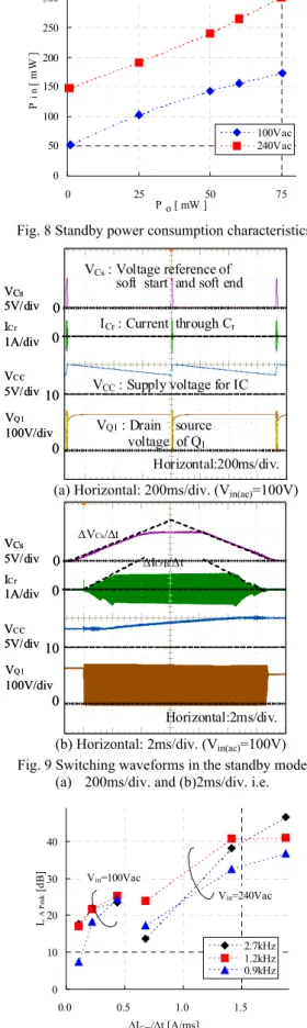
A. Standby power consumption characteristics
Figure 8 shows experimental results of the power consump- tion characteristics. The experimental conditions are as follows:
Input voltage V
in(ac)= 100V-240V, Output voltage rating V
Otyp=24V, Output Rating P
o(typ.)= 144W, Resonant Capacitor C
r=22nF, Reso- nant Inductance L
r= 320uH, Magnetizing Inductance L
m=1.8mH, Winding ratio of T
rT
NP1: T
NS1(=T
NS2): T
NP2: T
NP3:T
NP4= 59: 8: 5: 6: 6, Capacitance of the output C
CO=2200uF, Capacitance connected to V
CCwinding C
VCC=470uF, Capacitance at CS terminal C
CS= 0.56uF – 2uF, Charge and discharge current from CS terminal I
CS= 100uA
It is confirmed that the standby power consumption P
inun- der no load condition i.e. 0 mW of the output power P
Ois be- low 60mW at 100V AC input and 150mW at 240V AC input, respectively. When the P
Ois 50mW under the light load condi- tion, P
inis below 150mW and 250mW at 100V and 240V AC input, respectively.
0 50 100 150 200 250 300
0 25 50 75
P o [ mW ]
Pi n [ mW ]
100Vac 240Vac
Fig. 8 Standby power consumption characteristics
V
Cs5V/div I
Cr1A/div V
CC5V/div V
Q1100V/div
0 Horizontal:200ms/div.
0 0
10
I
Cr: Current through C
rV
Cs: Voltage reference of soft start and soft end
V
CC: Supply voltage for IC V
Q1: Drain source
voltage of Q
1V
Cs5V/div I
Cr1A/div V
CC5V/div V
Q1100V/div
0 Horizontal:200ms/div.
0 0
10
I
Cr: Current through C
rV
Cs: Voltage reference of soft start and soft end
V
CC: Supply voltage for IC V
Q1: Drain source
voltage of Q
1(a) Horizontal: 200ms/div. (V
in(ac)=100V)
V
Cs5V/div I
Cr1A/div V
CC5V/div V
Q1100V/div 0
Horizontal:2ms/div.
VCs
/t
0 0
10
ICrp
/t V
Cs5V/div I
Cr1A/div V
CC5V/div V
Q1100V/div 0
Horizontal:2ms/div.
VCs
/t
0 0
10
ICrp
/t
(b) Horizontal: 2ms/div. (V
in(ac)=100V) Fig. 9 Switching waveforms in the standby mode.
(a) 200ms/div. and (b)2ms/div. i.e.
0 10 20 30 40
0.0 0.5 1.0 1.5
L A Peak [dB]
2.7kHz 1.2kHz 0.9kHz Vin=240Vac Vin=100Vac
ICrp/t [A/ms]