Japan Advanced Institute of Science and Technology
JAIST Repository
https://dspace.jaist.ac.jp/
Title 熱電ナノ粒子の化学合成とナノ構造熱電材料の創製
Author(s) Nguyen, Thanh Mai Citation
Issue Date 2013‑09
Type Thesis or Dissertation Text version ETD
URL http://hdl.handle.net/10119/11561 Rights
Description Supervisor:前之園 信也, マテリアルサイエンス研究
科, 博士
Synthesis and Characterization of Nanoparticles and Nanostructured Materials for Thermoelectric Applications
NGUYEN THANH MAI
Japan Advanced Institute of Science and Technology
Synthesis and Characterization of Nanoparticles and
Nanostructured Materials for Thermoelectric Applications
by
NGUYEN THANH MAI
Submitted to
Japan Advanced Institute of Science and Technology In partial fulfillment of the requirements
For the degree of Doctor of Philosophy
Supervisor: Professor Dr. Shinya Maenosono
School of Materials Science
Japan Advanced Institute of Science and Technology
September 2013
i
Acknowledgment
This thesis could not be completed without the support and contribution of many people. I would like to thank Prof. Dr. Shinya Maenosono for supervise me during my research.
His encouragement, guidance and support always lead me ahead with my research. He creates a good research environment in the lab that I can study and enjoy my study time.
I highly acknowledge Prof. Dr. Kohki Ebitani for being my second supervisor. I learn from him many helpful things for my research and my life.
My thanks will go to Assoc. Prof. Dr. Mikio Koyano for his acceptance as my minor research project supervisor. His kindly guidance and discussions strongly contribute to the expansion of my knowledge to physic aspects of my work.
I would like to acknowledge the useful discussion and help from Prof. Hideo Iwasaki, Dr. Koichiro Suekuni, Dr. Tatsuya Murakami, Dr. Koichi Higashimine, Dr. Go Nakamoto from JAIST and Dr. Atsushi Yamamoto from AIST. They kindly cooperate with me in many of the technical issues and measurements presented in this thesis.
I would like to thank Dr. Derrick M. Mott for his support and discussion from the very beginning of my research in Japan as well as his correcting and proofreading my paper works.
I express my sincere gratitude to the former and current members of the Maenosono and Ebitani Lab for their support and sharing with me the studying time in the lab.
Finally, I would like to thank my family for their endless love and understanding for all hard and happy moment of my life.
Nguyen Thanh Mai September 2013
ii
Table of Contents
i) Acknowledgment ii) Table of Content
vi) Abbreviation and Symbol vii) List of Figure
xi) List of Table xii) Abstract
Chapter 1. General Introduction to Thermoelectric Materials and Research Objective 1
1.1. Introduction to Thermoelectric Materials ... 2
1.2. Thermoelectric Effect, Thermoelectric Efficiency and Its Limitation ... 3
1.3. Materials for Thermoelectric Applications ... 6
1.4. Solution for Improving the Thermoelectric Efficiency ... 7
1.4.1. Alloying ... 8
1.4.2. Phonon rattling in complex symmetric and crystal materials ... 9
1.4.3. Low dimensional materials ... 9
1.5. Chemical Synthesis of Nanoparticles for Thermoelectric Applications ... 11
1.5.1. Thermal decomposition method ... 12
1.5.2. Hydrothermal method ... 12
1.5.3. Solvent based reduction method ... 13
1.5.4. Important factors in the synthesis towards well-defined NPs for TE applications ... 14
1.5.5. Review on the chemical method to synthesize some representative NPs for TE applications ... 15
1.5.6. Thermoelectric properties of nanostructured TE materials synthesized using chemical methods ... 25
1.6. Research Objective ... 26
References ... 29
iii
Chapter 2. Study on Formation Mechanism and Ligand-directed Architectural Control of Nanoparticles Composed of Bi, Sb and Te: towards One-pot Synthesis of Ternary
(Bi,Sb)2Te3 Nanobuilding Blocks ... 34
2.1. Introduction ... 35
2.2. Experimental Section ... 37
2.2.1. Chemicals ... 37
2.2.2. Synthesis of NPs ... 38
2.2.3. Instrumentation and analysis conditions ... 38
2.3. Results and Discussion ... 39
2.3.1. Study of monometallic synthesis approach ... 40
2.3.2. Study of bimetallic synthesis approach ... 44
2.3.3. Summary of the mono- and bi-metallic synthesis studies ... 51
2.3.4. Study of trimetallic synthesis approach ... 52
2.3.5. Summary of the nanoparticle formation mechanism ... 55
2.4. Conclusion ... 56
Acknowledgment ... 57
References ... 57
Chapter 3. Chemical Synthesis of BiSbTe Nanoparticles with Composition and Shape Manipulation ... 59
3.1. Introduction ... 60
3.2. Experimental Section ... 61
3.2.1. Chemicals ... 61
3.2.2. Synthesis of BiSb NPs ... 62
3.2.3. Synthesis of BiSbTe NPs ... 62
3.2.4. Instrumentation and analysis conditions ... 63
3.3. Results and Discussion ... 63
3.3.1. Binary solid solution BiSb NPs with controllable composition and morphology ... 63
3.3.2. Seed mediated growth of the ternary solid solution BiSbTe NPs ... 69
3.4. Conclusion ... 70
Acknowledgment ... 71
References ... 71
iv
Chapter 4. One-pot Chemical Synthesis of Zinc Antimonide Nanoparticles as Building
Blocks for Nanostructured Thermoelectric Materials ... 73
4.1. Introduction ... 74
4.2. Experimental Section ... 75
4.2.1. Chemicals ... 75
4.2.2. Synthesis of Zn-Sb NPs ... 75
4.2.3. Synthesis of Sb NPs ... 75
4.2.4. Synthesis of Zn NPs ... 76
4.2.5. Instrumentation and analysis conditions ... 76
4.3. Results and Discussion ... 77
4.3.1. Morphology, composition, structure and surface properties of Zn-Sb NPs .. 77
4.3.2. Seebeck coeffiecient of the powder of Zn-Sb NPs ... 82
4.4. Conclusion ... 83
Acknowledgment ... 83
References ... 83
Chapter 5. Scaled-up Chemical Synthesis of Zn-Sb Nanoparticles and Thermoelectric Properties of Zn-Sb Nanostructured Materials ... 85
5.1. Introduction ... 86
5.2. Experimental Section ... 87
5.2.1. Chemicals ... 87
5.2.2. Large scale synthesis of Zn-Sb NPs ... 87
5.2.3. Making the nanostructured pellet ... 88
5.2.4. Instrumentation and analysis conditions ... 89
5.3. Results and Discussion ... 90
5.3.1. Large scale chemical synthesis of Zn-Sb NPs ... 90
5.3.2. Zn-Sb NPs after thermal treatment ... 96
5.3.3. Zn-Sb pellet after hot pressing ... 98
5.3.4. Thermoelectric properties of the Zn-Sb nanostructured pellet ... 101
5.4. Conclusion ... 106
Acknowledgment ... 107
References ... 107
v
Chapter 6. Conclusion and Prospects ... 109
Appendix I ... 111
Appendix II ... 120
Appendix III ... 134
Appendix IV ... 136
Appendix V ... 139
List of Publication ... 143
Abstract of Subtheme Research ... 147
vi
Abbreviation and Symbol Abbreviation
DT Decanethiol
EDS Energy Dispersive X-ray Spectroscopy HAADF High Angle Annual Dark Field
HR-TEM High Resolution Transmission Electron Microscopy ICP-MS Inductively Couple Plasma - Mass Spectroscopy
ICP-OES Inductively Couple Plasma – Optical Emission Spectroscopy ND, NDs Nanodisc, Nanodiscs
NP, NPs Nanoparticle, Nanoparticles NW, NWs Nanowire, Nanowires
OAC Oleic Acid
OAM Oleylamine
SEM Scanning Electron Microscopy
STEM Scanning Transmission Electron Microscopy
TE Thermoelectric
TEM Transmission Electron Microscopy TGA Thermal Gravimetric Analysis XPS X-ray Photoelectron Spectroscopy XRD X-ray Diffraction
Symbol
α Seebeck coefficient κ Thermal conductivity ρ Electrical resistivity σ Electrical conductivity
λ Wavelength
vii
List of Figure
Figure 1.1. Schematic illustration of Seebeck effect (A) and a gas diffusion model to explain the voltage arises from the temperature gradient applied to a p-type semiconductor (B) ... 4 Figure 1.2. Thermoelectric generator composed of n-type and p-type semiconductors based on Seebeck effect ... 5 Figure 1.3. Contribution of phonons with different mean free paths to the cumulative lattice thermal conductivity value for PbTe... 8 Figure 1.4. Hydrothermal reaction to synthesize PbTe NWs and TEM images of PbTe NWs ... 12 Figure 1.5. TEM images of Bi2Te3/Te nanowires and Bi2Te3/Sb2Te3 nanodiscs synthesized using oleic acid/oleylamine and decanethiol as capping ligands respectively ... 13 Figure 1.6. Schematic illustration of the chemical method to synthesize Bi2Te3 nanotube using Te nanowire (NW) template via Kirkindall effect ... 14 Figure 1.7. Schematic illustration of utilizing capping species to direct the shape formation of NPs via control the kinetic growth of NPs in the chemical method ... 15 Figure 1.8. SEM images of (a) Bi2(Te,Se)3, (b) (Bi,Sb)2Te3 aggregated nanocrystals synthesized by aqueous chemical route adapted from ref. 65 and (c) TEM image of (Bi,Sb)2Te3
powder by hydrothermal synthesis adapted from ref. 66 ... 18 Figure 1.9. TEM images of (a) Bi0.5Sb1.5Te3.0 NPs adapted from ref. 68, (b) Bi1.0Sb1.0Te3.0
nanosheets and (c) Bi1.7Sb0.4Te3.0 nanoplatelets synthesized by ligand assisted solvothermal route adapted from ref. 15 ... 19 Figure 1.10. TEM images of Zn4Sb3 NPs obtained from the synthesis in solution adapted from ref 95 ... 23 Figure 1.11. Summary of the issues and research objectives ... 27
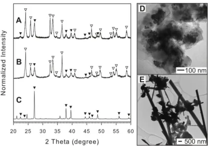
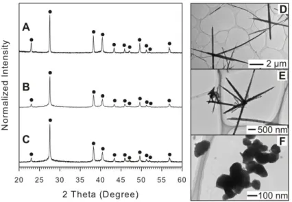
Figure 2.1. XRD patterns and TEM images of materials synthesized using BiCl3 and OAM (A and D), OAC/OAM (B), and DT (C and E) ... 41 Figure 2.2. XRD patterns and TEM images of Sb NWs synthesized using OAM (A and C) and OAC/OAM (B and D). In the case of using DT, no solid particles can be obtained ... 43 Figure 2.3. XRD pattern and TEM images of resulting Te NPs synthesized using OAM (A and D), OAC/OAM (B and E), and DT (C and F) ... 44 Figure 2.4. XRD patterns and TEM images of the Bi-Sb NPs synthesized using OAM (A and D), OAC/OAM (B and E), and DT (C and F). G is the HR-TEM image of Bi-Sb NPs synthesized using OAM. ... 46 Figure 2.5. Relationship between the lattice spacing of (012) crystal plane and molar composition of BiSb alloy synthesized using OAM (Bi70Sb30) and OAC/OAM (Bi95Sb5) .... 47
viii
Figure 2.6. XRD patterns and TEM images for Bi-Te materials synthesized using OAM (A and D), OAC/OAM (B and E), and DT (C and F) ... 49 Figure 2.7. XRD patterns and TEM images for Sb-Te materials synthesized using OAM (A and D), OAC/OAM (B and E), and DT (C and F) ... 51 Figure 2.8. TEM (A-C) and HR-TEM (D-E) images of trimetallic NWs synthesized using OAM as capping species with 1:1 molar ratio of precursors and OAM ... 53 Figure 2.9. XRD patterns of trimetallic NWs synthesized using OAM as capping species with 1:1 molar ratio of precursors and OAM ... 54 Figure 2.10. The illustration of the formation mechanisms for (A) Te/Bi2Te3/Sb2Te3 phase- segregated NDs synthesized using DT as a capping system and for (B) Te/(Bi,Sb)2Te3 NWs synthesized using OAM as a capping system ... 56
Figure 3.1. TEM images of BiSb NPs synthesized using approach I (upper row A-C) and II (lower row D-F) with Bi:Sb molar feeding ratio of 1:2, 1:1 and 2:1 (from left to right) ... 63 Figure 3.2. TEM images of single elemental Bi NPs (A, B) and Sb NPs (C, D) synthesized using synthesis approach I (left) and II (right) respectively. ... 64 Figure 3.3. Size distributions of BiSb NPs synthesized using approach I (upper row A-C) and II (lower row D-F) with Bi to Sb molar feeding ratio of 1:2, 1:1 and 2:1 (from left to right) . 65 Figure 3.4. Illustration for the correlation between size and feeding ratios (then composition) of resulting BiSb NPs due to the differences in the nucleation and growth rate of Bi and Sb under the reaction conditions used in the injection method (synthesis approach II) ... 65 Figure 3.5. XRD patterns of BiSb NPs synthesized using approach I with BiCl3:SbCl3 molar feeding ratio of (A) 1:2, (B) 1:1 and (C) 2:1 ... 66 Figure 3.6. XRD patterns of BiSb NPs synthesized using approach II with BiCl3:SbCl3 molar feeding ratio of (A) 1:2, (B) 1:1 and (C) 2:1 ... 66 Figure 3.7. Relationship between the lattice spacing of (012) crystal plane of the synthesized BiSb NPs with the molar feeding ratios of BiCl3 to SbCl3 equal to 1:2, 1:1 and 2:1 and the corresponding composition of NPs measured by EDS ... 68 Figure 3.8. Relationship between the Bi content in NPs and the input moles of Bi precursor (in percentage) ... 68 Figure 3.9. TEM images of BiSb seed NPs redispersed in diphenylether (A) and BiSbTe NPs synthesized at 195 oC (B), using OAM as the reducing agent and capping ligand with the seed’s composition of Bi74Sb26 ... 70
ix
Figure 3.10. XRD patterns of BiSbTe NPs synthesized at 195 oC, using OAM as the reducing agent and capping ligand. The BiSb seed NPs were synthesized with BiCl3:SbCl3 feeding ratio
of 1:1. ... 70
Figure 4.1. Schematic illustration of the configuration for Seebeck measurement ... 77
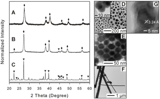
Figure 4.2. TEM image (A) and XRD pattern (B) of Sb NPs... 78
Figure 4.3. TEM image (A) and XRD pattern (B) of Zn NPs. ... 78
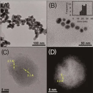
Figure 4.4. TEM images of Zn-Sb NPs (A, B) (the inset in (B) shows the size distribution of NPs), high-resolution TEM (C) and HAADF-STEM image (D) of a single Zn-Sb NP. ... 78
Figure 4.5. XRD pattern of Zn-Sb NPs ... 79
Figure 4.6. XPS spectra of Zn-Sb NPs, (A) Zn 2p and (B) Sb 3d areas ... 80
Figure 4.7. XPS spectra of (A) Zn 2p area of Zn NPs and (B) Sb 3d area of Sb NPs ... 80
Figure 4.8. (A) HAADF-STEM and (B-D) EDS elemental mapping images of a Zn-Sb NP: overlay (B) of Zn K edge (C) and Sb L edge (D), (E) the EDS line profile at the center of the NP as indicated by a yellow line in (a). Dashed and solid lines represent raw and low-pass- filtered profiles, respectively. ... 82
Figure 5.1. Photograph of the reactor after 1 hour of reaction with the black dispersion of the resulting NPs in di-phenylether. The reaction solution volume is about 1070 mL ... 88
Figure 5.2. TEM images of (A) Sb seed NPs and (B-I) Zn-Sb NPs synthesized using different molar feeding ratios of Zn to Sb precursors... 91
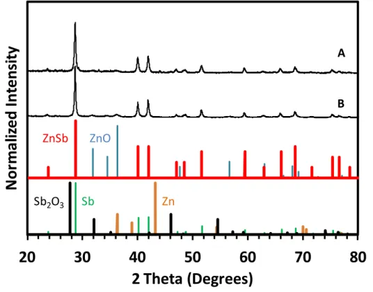
Figure 5.3. XRD pattern of the as-synthesized Zn-Sb NPs using different molar feeding ratios of Zn to Sb precursors ... 94
Figure 5.4. XPS spectra of resulting NPs from Sample III with composition of Zn42Sb58 (upper row) and Sample IV with composition of Zn45Sb55 NPs (lower row): the narrow scan areas of Sb 3d and Zn 2p ... 95
Figure 5.5. TGA curve for the Zn-Sb NPs after 6 hours annealing at 366 oC ... 96
Figure 5.6. XRD pattern of Zn-Sb NPs after thermal annealing for Sample III (A) and IV (B) ... 97
Figure 5.7. XRD pattern of Zn-Sb pellets after hot pressing of Sample III (A) and IV (B) ... 99
x
Figure 5.8. Upper row: TEM sample preparation from the pellet in which FIB stands for focus ion beam, the technique used to prepare thin film sample for TEM observation; the blue arrows indicate the position from the surface of the pellet; and the TEM image shows small grain size in the pellet. Lower row: dark field (HAADF) image and elemental mapping images for Sb L, Zn K, O K ... 100 Figure 5.9. Temperature dependence of the thermoelectric properties of Zn-Sb nanostructured pellet prepared from Sample III ... 102 Figure 5.10. Temperature dependence of the thermoelectric properties of Zn-Sb nanostructured pellet prepared from Sample IV ... 103 Figure 5.11. Schematic illustration of the micro-structure of the pellet ... 104
xi
List of Table
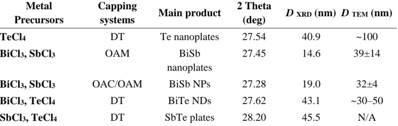
Table 2.1 Main products synthesized using a single metal precursor ... 40 Table 2.2 Main products synthesized using two different kinds of metal precursors ... 45 Table 2.3 Mean crystalline size calculated for NPs based on XRD pattern and Scherrer's formula ... 48 Table 3.1 Summary of main results in composition, XRD peak position of (012) crystal plane and sizes of NPs for each synthesis approach ... 67 Table 5.1 Summary of the composition, phases and sizes for the as-synthesized Zn-Sb NPs using different molar feeding ratios of the metal precursors ... 92 Table 5.2 Summary of the composition of Zn-Sb NPs and pellets and the bulk properties the pellets ... 98 Table 5.3 Thermoelectric properties of related materials. The data if not mentioned more were given at RT ... 105
xii
Abstract
Thermoelectric (TE) materials are interesting research field for energy conversion applications such as cooling devices, power generation, energy harvesting materials. Because TE materials can enable the direct alternative conversion between poor-quality thermal energy and high-quality electric energy, the renewal of these materials can make them become potential candidate for a next generation technology of waste heat recovery. TE materials with phonon-glass electron-crystal (PGEC) property have been recognized as one of the most promising approaches to improve the TE efficiency for practical applications and introducing desired nanostructure into TE materials is one way to create PGEC materials.Because of the capability of well control morphology and nanostructure, chemical synthesis is interesting for producing nanoparticles (NP)s with tailorable characteristics for TE applications. Furthermore, the chemical synthesis could be scaled up to obtain large amount of NPs for creating nanostructured TE materials.
The purpose of this research is to develop the chemical synthesis approaches towards nanoparticles and nanostructured materials for TE applications. With this purpose, my research will address the issues regarding NPs synthesized via chemical methods in order to offer scalable and economic comparative syntheses with capability of creating compounds and alloys with tailorable characteristics in nanoscale regime. The NPs which I focus on include Bi- Sb-Te based ternary alloys and Zn-Sb alloys which can be applied for room temperature to 400 oC and are challenging for chemical synthesis.
(1) Synthesis and formation mechanism to control the composition and morphology of solid solution BiSbTe NPs The modified polyol method was utilized to synthesized BiSbTe containing NPs via a one-pot chemical reaction.
The resulting NPs show various morphologies (nanowires, nanodiscs, nanodiscs grew on NWs) associated with nature of the capping ligands used in the synthesis and the phase segregation occurs in each case. Because of the complicated interactions between metal precursors and capping ligands as well as the metal interaction in the one-pot reaction, a systematic investigation of the synthesis of monometallic, bimetallic and trimetallic NPs was conducted to elucidate the NP’s formation mechanism. The results of the investigation indicate that using DT as capping ligand, Te can act as the catalyst for the formation of Bi2Te3 and Sb2Te3 and the strong interaction between Te and Bi and/or Sb precursor complex results in the phase segregation of the resulting BiSbTe containing NPs. On the other hand, using OAM as the capping species, BiSb NPs (alloy) can be formed and the interaction between BiSb and Te NPs in the solution can result in the formation of ternary BiSbTe NPs. Based on the NP’s formation mechanism, the one-pot synthesis is performed with tri- molecular precursors in OAM to achieve ternary BiSbTe NWs. To further control the morphology and composition of ternary BiSbTe NPs, the chemical synthesis was modified in which BiSb alloy NPs with tailorable composition first prepared in the presence of OAM and used as the seed to grow ternary solid solution BiSbTe NPs. The resulting NPs are ternary alloy of Bi, Sb and Te and the ratios of Bi:Sb and the morphology of the seeds were maintained in the BiSbTe NPs. The results of these studies offer the fundamental understanding of the NPs’ formation mechanism and the basic knowledge to synthesize NPs with controllable morphology and composition.
(2) Zn-Sb NPs: chemical synthesis and large scale reaction to create the nanostructured Zn-Sb materials.
A chemical synthesis with multiple steps in one-pot reaction was designed via the formation of Sb NPs as the seed followed by the reduction of Zn on surface of Sb NPs and alloying to form Zn-Sb NPs. The careful investigation using TEM, XRD, EDS, XPS, STEM-HAADF reveals the complex structure of Zn-Sb NPs with core-shell like morphology and the opposite composition distribution of Zn and Sb from the core to the shell of single NP. The enhancement of oxidation stability of Zn-Sb NPs is associated with the alloy formation.
The nanostructured Zn-Sb materials were prepared from Zn-Sb NPs obtained in the large scale synthesis (after surface treatment) via hot-pressing. The Zn-Sb pellets still possess the nanograinboundary and the TE properties of the pellets were investigated. The results indicated that the pellets have semiconducting properties with good electrical conductivity, low thermal conductity and Seebeck coefficient similar to Sb, which arises from the existence of Sb phase and Zn-Sb phase together with ZnO in the pellet. Even though the TE efficiency is not significant, the research exhibits the capability of utilizing NPs as the building block for creating nanostructured TE materials. Further study on the reaction and pressing conditions can help to improve the TE efficiency.
Key word: thermoelectric, nanoparticles, semiconductor, chemical synthesis, alloy
1
Chapter 1
General Introduction to Thermoelectric Materials and Research Objective
This chapter will give a general introduction to the thermoelectric (TE) effect, TE materials and the challenges to make TE materials practical available for energy conversion.
The studies on improving TE efficiency, the center of the current research on TE materials, are briefly reviewed. We then focus on the nanoparticles as a potential candidate for improving TE performance with an overview on the chemical synthesis approach to get nanoparticles as promising building block for creating TE materials. The difficulties and strategy to synthesize nanoparticles with well-defined structure and tunable properties for TE applications will be reviewed. The chapter will conclude with the objective of the research.
2
1.1. Introduction to Thermoelectric Materials
Energy is considered to be the blood of the planet because of the fact that all activities of living thing require energy. The energy sources consist of two types, one is the long term energy (eternal energy) such as solar energy or earth heat and the other created from solar energy and stored in biomass and underwent a chemical and physical transition such as charcoal, petroleum, natural gas... The later is ready to use but it is expected to be quickly run out in the future at the current demand of energy. Furthermore, using these energy sources always result in the CO2 emission and greenhouse effect which damages the environment and sustainable development. A new policy and research should be devoted to solve these problems. One direction mainly focuses on creating new energy sources such as making use of reusable energy from biomass, fuel cell, solar cell… Researchers all over the world are doing their best for those green energy sources widely and practically available to replace oil and charcoal. The other direction which also attracts much of consideration is to improve the efficiency of using energy in the world (in other words, saving energy). It would be significant if we take into account the current efficiency of using energy where about 30 % of energy will be ready to use while large amount of energy releases as heat waste. In term of power generation as well as improving the energy usage efficiency, thermoelectric (TE) materials known to be one potential candidate can converse heat (in general) and/ or heat lost to electricity. In other words, these materials enable direct alternative conversion between poor- quality thermal energy and high-quality electric energy. Especially, the reuse of waste heat will be significant with the renewal of these materials to become a next generation technology.
Another advantage of TE materials is associated with the fact that TE materials can help to reduce the impact on the environment via diminishing CO2 emission during the energy conversion processes. The advantage is also worth when TE materials are utilized as electronic cooling devices and equipments when apply the current to generate the thermal difference at their ends without moving part or Freon generation. Therefore, to solve the energy and environmental issues, TE materials are expected to be very important candidate.1-7
Back to the history of TE materials, the underlying physics of TE materials, called thermoelectric effects including Seebeck effect, Peltier effect, are well known for a long time.
However, since Seebeck effect and Peltier effect were separately discovered in 1821 and 1834 respectively which served as basic principles for TE materials, until second half of the 20th century, TE materials for energy conversions became practical.3,4 The great consideration and
3
extensive researches were put on this field which resulted in the finding of Bi and Bi-Sb alloys, Bi2Te3 based alloys and PbTe compound as well as Si-Ge alloys as the state of the art materials for specific temperature ranges.1,5,7 Those studies also expanded a huge knowledge of TE properties and materials characteristics relation, synthesis techniques and characterization methods. However from those studies, a limitation of TE efficiency is found and set a big challenge for not only the wide application of TE materials in terms of energy conversions but also the further study in this field. By the 1970s, less research effort was made in TE material and seemed to be stopped because it was considered as a mature field. Two decades later, in the 1990s, when the energy crisis become serious and requirement for higher TE efficiency became crucial for the future development, TE research had been brought back with great of interest. Along with the renewing of TE research, many new findings in theoretical and calculation aspect, thin film, nanotechnology and new concept for materials have been discovered and evidenced, which expected to open new windows for higher TE performance.
The following part of this chapter will overview the underlying principle of TE effect, thermoelectric efficiency and its limitation, the materials for thermoelectric application, the proposed solutions for improving TE efficiency. A part of this chapter will focus on the chemical synthesis approach to get TE nanoparticles (NP)s as promising building block for TE application. This chapter will end with the research area and the objective of the study presented in the thesis. The characterization methods of low dimensional materials and the measurement of TE properties are important for study in field of NP for TE applications will be given in the Appendix I.
1.2. Thermoelectric Effect, Thermoelectric Efficiency and Its Limitation
Thermoelectric effects refer to the effects in which thermal energy converts to electricity and vice versa. The Seebeck effect, named after the physicist Thomas Johann Seebeck, occurs when a temperature gradient between the junctions of two conductors connected each other raises a voltage between two junctions. This effect is familiar with all technicians and scientists who work with a thermal couple to measure temperature. The Seebeck effect can be expressed via an integral form relates the voltage V appears at temperature difference ΔT: V = αabΔT, where αab is the Seebeck coefficient of two junctions between conductors a and b (Fig. 1.1A).
4
Figure 1.1. Schematic illustration of Seebeck effect (A) and a gas diffusion model to explain the voltage arises from the temperature gradient applied to a p-type semiconductor (B).
The Peltier effect which named after Jean Charles Athanase Peltier exhibits the phenomenon when a current passing though the junction between two conductors creates the temperature different at the two ends of the junction. The integral form of the Peltier effect is πab = q/I, where q is the heating rate (cooling rate) at one of the junctions when an electric current I passes round the circuit and πab is the Peltier coefficient for these two junctions. The Seebeck effect and Peltier effect are reversible phenomenon and closely related to each other via the Kelvin relationships: πab = αabT. It is noted that these two thermoelectric effects are defined for two junctions between two conductors, but the two coefficients are properties of the bulk materials which have the absolute coefficient (αa, πa for examples) and αab and/or πab
equal to the different of the absolute coefficients of two conductors (αab = αa - αb, πab = πa - πb).
The Seebeck coefficient is often regarded as thermopower of the materials and can be measured easier than the Peltier coefficient. The Seebeck and Peltier effects can be imagined with consideration that electrons/holes diffuse under temperature gradient or move in the electric field as gas model (Fig. 1.1B).
The efficiency of TE materials is defined by the useful work (w) divided by the heat (q) from the heat source: w/q. The temperature different between the heat source (TH) and the sink (TC) (TH-TC) results in the electromotive force V = αab(TH-TC). The current of the circuit I, equals to V/(R+RL) where R is the resistance of TE generator and RL is the resistance of the load. The heat is the sum of the heat lost by thermal conduction of the TE generator and the heat compensates for Peltier cooling of the hot junction when the current passes through:
q = K(TH-TC) + αabITH (1) The highest efficiency (ηmax) was first given by Ioffe as follows:
5 ηmax = (𝑇𝐻−𝑇𝐶)
𝑇𝐻
(1+𝑍𝑇)1/2
𝑇𝐶/𝑇𝐻+(1+𝑍𝑇)1/2 (2)
where T = (TH+TC)/2, and Z equals to (αab2/KR) which is the figure of merit of the TE generator (Fig. 1.2). It is noted that (TH-TC)/TH is the maximum efficiency of an ideal thermodynamic machine (Carnot efficiency). Therefore, the highest TE efficiency could be reached when Z value becomes very large. The efficiency of TE materials strongly depends on the Z (ZT) value and the Z value depends on the properties of both materials which form the TE generator. The figure of merit Z of the TE generator when it reaches the optimum value is given by:
𝑍 = (𝛼𝑎−𝛼𝑏)2
[(𝜎𝑎𝜅𝑎)1/2+(𝜎𝑏𝜅𝑏)1/2]2 (3) where 𝜅a, 𝜅b is the thermal conductivity of two branches of TE generator.
Figure 1.2. Thermoelectric generator composed of n-type and p-type semiconductors based on Seebeck effect.
For a single material, the figure of merit is defined as 𝑧 = 𝛼2𝜎/𝜅 (where σ is the electrical conductivity, κ is the thermal conductivity and α is the Seebeck coefficient of the material) which is convenient in investigation of the TE materials. The figure of merit has the dimension of inverse temperature, and when times it with absolute temperature (normally operating temperature range) we have the dimensionless figure of merit, zT, which is commonly used. The other definition of figure of merit is as the ratio of power factor to thermal conductivity. The power factor (𝛼2𝜎) depends on the electronic properties of the material while the thermal conductivity is sum of lattice and electrical thermal conductivity, 𝜅L and 𝜅e
respectively. It is noted that the electrical thermal conductivity always exists and it is in
6
relationship with the electrical conductivity expressed in Wiedemann-Franz law: 𝜅e = LσT, where L is the Lorentz number which is a constant for metal and depend on the Fermi level for a semiconductor (SC). For this reason, each increase or decrease of electrical conductivity always causes the corresponding increase or decrease of thermal conductivity, which make the ratio of σ/κe nearly constant. Moreover, the Seebeck coefficient, α, is also in a relation with the electrical conductivity, σ, because an increase in α of often gives a certain decrease of σ. The interrelation of parameters determined thermoelectric efficiency therefore sets a limitation (zT about 1) which is difficult to overcome.
1.3. Materials for Thermoelectric Applications
A good material for TE applications must satisfy the following requirements of high enough Seebeck coefficient, high electrical conductivity and low thermal conductivity.
Because an increase in α often leads to the decrease of σ and the decrease of σ results in the decrease of the electronic contribution to κ as displayed in Wiedemann-Franz law. Hence, for bulk materials, these requirements themselves make a fundamental challenge for searching a good TE material. Metals and their alloys generally have very low α (less than some tens of microvolts per Kelvin) and the ratio of σ to κ nearly the value given by Wiedemann-Franz law, which is all together resulting in much less than unity of the dimensionless TE figure of merit (zT).
Since semiconductors were discovered, the higher Seebeck coefficient of milivolts per Kelvin was found in some SCs.8 However, SCs with enhanced Seebeck coefficient still displayed a small value of the ratio between electrical conductivity and thermal conductivity due to the fact that they have low electrical conductivity and the dominant of the lattice thermal conductivity. The improvement in the ratio between electrical and thermal conductivity nearly the value given in Wiedemann-Franz law in some of SCs make them become the current used TE materials. In the classical approximation,3 the zT value was estimated by:
𝑧𝑇 = [𝜂−(𝑟+
5 2)]2
(𝛽exp𝜂)−1+(𝑟+52) (4)
where η is the Fermi energy divided by kT (different from the efficiency in eq.2), r is a scattering parameter that describes the way in which the relaxation time for the carriers varies with energy and r often lies between -1/2 and 3/2, the extremes corresponding to acoustic-mode lattice scattering and ionized-impurity scattering. β was given by:
7 𝛽 = 5.745 × 10⁻⁶ 𝜇
𝜆𝐿(𝑚∗
𝑚)3/2𝑇5/2 (5)
where µ is the carrier mobility, m and m* is the mass of a free electron and the effective mass of the carriers. For the optimum value of zT, the quantity β should be as high as possible.
However, it is found that for known materials, β is less than 0.5.
The calculations based on classical statistics as well as Fermi-Dirac statistics are in good agreement in indicating the zT can reach the optimum in SCs with high carrier mobility, large effective mass, and low thermal conductivity. It also requires a large enough energy gap, Eg, for the negligible of the concentration of the minority carrier when the Seebeck coefficient is optimized. In the classical SCs, the maximum value of Seebeck coefficient at given temperature is equal to Eg/2eT, where e is the electronic charge. The Seebeck coefficient can be calculated using Fermi-Dirac statistics, and the optimum value is close to ± 200 µVK-1.3
1.4. Solutions for Improving the Thermoelectric Efficiency
The solutions for improving TE efficiency include the methods to obtain materials displaying good Seebeck coefficient, electrical conductivity and low thermal conductivity, on the other words, to reduce the lattice thermal conductivity without much decrease of the power factors, or improvement of power factor of the existing materials without increasing much of thermal conductivity. The current researches in the field of TE indicate that the phonon glass electron transmission materials which offer low thermal conductivity as glasslike materials and high electrical conductivity as metal should be ideal for high performance thermoelectricity.9 Introducing the mechanism to lower the thermal conductivity via effective and selective phonon scattering therefore becomes very important to obtain the ideal TE materials. Because the heat carried by phonon often has a band spectrum of mean free path (MFP)10 which can be scattered in different mechanisms (Fig. 1.3), the study and combination of scattering phonons with short, medium, and long MFP can result in extremely low thermal conductivity at the same extent of electrical structure. The following reviews the methods to effectively scatter heat carried by phonon at different length scale (of the MFP) while not much affect on the electrical conductivity of the materials.
8
Figure 1.3. Contribution of phonons with different mean free paths to the cumulative lattice thermal conductivity value for PbTe adapted from ref. 10.
1.4.1. Alloying
This method was first proposed by Ioffe and his colleagues based on the prediction that alloying allows introducing the short range disturbance to significantly scatter phonon but the maintaining the long range order to prevent the scattering of electrons and holes.8 As a result, the alloys exhibit much lower thermal conductivity than their constituents without decreasing of electrical conductivity. This approach serves as one efficient method providing the most improvement of zT in 1950s -1960s and find its significant in Bi2Te3 based materials (now mostly in solid solution with Sb2Te3 or Bi2Se3 to form one of the best p- and n-type SCs for TE application at room temperature up to 200 oC ), Pb-Te (often in solid solution with SnTe, PbSe to form one of the best p- and n-type SCs for TE application at intermediate temperature above 200 oC to 500 oC), and Si-Ge alloys (above 500 oC to 1000 oC) which are now used as materials for TE generation. For example, the alloy Bi0.5Sb1.5Te3 and Bi2Te2.7Se0.3 show the figure of merit, z, increase to 3.3x10⁻³ K-1 compared to z of 2x10⁻³ K-1 for Bi2Te3. Another example is about Si-Ge alloy at 300 K the κ values for Si and Ge are of 113 and 63 Wm-1K-1 respectively while a solid solution of Si and Ge with composition of Si0.7Ge0.3 has κ of only 10 Wm-1K-1.
The underlying mechanism of the thermal conductivity reduction is the phonon scattering due to mass fluctuation entire the solid solution. The alloying allows the effectively scattering of phonon with short mean free paths in the order of subnano to several nanometers.
(Phonon scattering mechanisms in crystal structure materials: the decrease of thermal conductivity of crystal materials is often due to the phonon-phonon scattering, phonon-
9
impurity scattering, phonon-boundary scattering. The first one was further divided into normal phonon scattering and Umklapp scattering where the phonon momentum was transferred to the lattice causing the resistance to the heat flow. The phonon-phonon scattering is important contribution to heat resistance at room temperature due to the Umklapp scattering, but phonon impurity scattering more dominant as lowering the temperature. At low temperature, phonon- boundary scattering contribute to the decrease of thermal conductivity (the MFP of phonon is comparable to the grain size of materials) and this kind of scattering is temperature independence. Therefore, at low temperature, the thermal conductivity is proportional to T3 as the same as specific heat.)
1.4.2. Phonon rattling in complex symmetric and crystal materials
In 1990s, Slack suggested the concept of “phonon glass electron crystal” (PGEC) as the criteria for good TE materials.9,11,12 His idea of such TE materials becomes somewhat practical presence in materials exhibiting the complex symmetry and crystal structure with “cages” or
“tunnels” large enough for atoms located inside to rattle but do not destroy the favorable electronic structure. The rattling centers (atoms) effectively scatter phonon for which the thermal conductivity is glasslike while allows the electron pass through the crystal lattice, displaying the PGEC structure. The “phonon rattling” concept proposed to reduce the lattice thermal conductivity in the crystal materials with high power factor is important as it had contributed to the great improvement of zT observed in the history of TE materials where many solid systems were found to possess zT values over 1 such as skutterudites and clathrates based on this standpoint.9,11-13 However, it is worth to emphasize that even the ideal PGEC material is still not practical presence, the enhancement of zT due to the rattling process in complex symmetric materials is a good theoretical guidance for researchers in searching effective TE materials based on lowering the thermal conductivity while maintaining a good electrical conductivity.
1.4.3. Low dimensional materials
Low dimensional thermoelectricity refers to two important strategies to improve zT value including: (i) offer large area of boundary for phonon-boundary scattering even at room temperature if the size of materials smaller or comparable with the mean free path of phonon, which results in extremely low κ, while still allows carrier transmission and (ii) improve α and somewhat decoupling α and σ via the quantum confinement effect theorized by Hick and
10
Dresselhaus in which the increase of the density of states near the Fermi energy leads to the enhancement of α and the low dimensionality offer the possibility to tailor the electronic structure to decouple the α and σ.14,15 The first advantage of the low dimensionality is based on choosing a suitable size of materials that allow the boundary effectively scattering phonon than electron giving rise in the σ/κ ratio.16-22 The experimental results in Bi2Te3-Sb2Te3
superlattices17 and nanostructured TE materials can clearly demonstrate this theoretical standpoint. The second aspect of low dimensionality regarding the enhancement of α arises from the increase of the density of states near the Fermi level due to the confinement effect.14,15 It was proved in the PbTe-Pb1-xEuxTe quantum well superlattices where the increase of α directly relates to the increase of density of state at each subband edge.3 Furthermore, the experimental results for n-type PbTe agree well with the theoretical calculation results that α2n, where n is the carrier concentration, also increase with the size decreases of PbTe. Another example is the size dependent semimetal-semiconducting transition due to the quantum confinement effect when the decrease of the size of Bi from the bulk to nano regime leads to the increase in Seebeck coefficient and the capability of tuning its electronic structure from semimetal into SC. These results indicate the possibility of decoupling the interrelated parameters, which determine TE efficiency, in low dimensional materials to obtain enhanced zT values.3
Other phenomena displaying in low dimensional materials can also contribute a part to the decoupling and somewhat independently modifying α, σ, κ are energy filtering, carrier pocket engineering.
The theory of low dimensionality (nano regime) for enhanced TE efficiency and the experimental achievements of improved zT values arising from decreasing the size of the state of the art TE materials make this research field become more and more promising for advanced TE materials. As mentioned before in this section, the much higher zT can reach by the combination of the low dimensionality (current approach) with alloying and/or complex structure and symmetry which is the main origin of the high zT in most of the bulk state of the art TE materials. Therefore, introducing low dimensionality (nanostructure) into state of the art TE materials has been active research topic in the field of advanced TE materials. Synthesis of these advanced materials, however, associates with a lot of difficulties regarding precise control the dimensions, nanostructure, composition, surface properties and so on due to its essential importance for TE efficiency improvement. Therefore, the following part of the thesis is devoted to overview the synthesis of nanoparticles (NP)s for TE applications, especially the
11
chemical synthesis which displays high capability of tailoring NPs characteristics compared to physical methods, its advantages, achievements and challenges.
1.5. Chemical Synthesis of Nanoparticles for Thermoelectric Applications
Regarding the synthesis method for TE materials, physical methods are dominant in producing bulk TE materials. In preparation of NPs for TE applications, there are two main methods categorized based on the starting materials and pathways used to create NPs: first, start with bulk materials, using physical method to reduce size of the bulk (top down methods) and second, start with the molecules and using molecules to build up the nanostructure (bottom up methods).23 The physical approaches include: alloying, melting, zone-melting, cold/hot- pressing, grinding, spark plasma sintering, crystal growth techniques, molecular beam epitaxy, molecular vapor deposition. Other approaches combine the physical and chemical methods such as electro-chemical synthesis, sono-chemical synthesis also work in producing TE NPs.
However, in terms of large scale synthesis, environmentally benign technique and manipulation NPs’ characteristics such as size, shape, composition, nanostructure, surface properties, and so on, there are some degrees of difficulty regarding the physical approaches which often require intensiveenergy, normally high temperature, some time high degree of vacuum level and expensive apparatus. Chemical synthesis, on the other hand, serve as a bottom up method, can offer host of advantages in tailoring NPs’ characteristics and potential to obtain large amount of products at comparative cost.24,25 As the characteristics of NPs are crucial important parameters affecting on the TE properties of their nanostructured materials, the good manipulations on those parameters have received great of interest. Hence, focusing on the chemical methods to control the NPs’ characteristics for advanced TE materials, a review is provided for the chemical methods, the key factors to obtain well-defined nanostructure, the capability and current difficulties when using chemical techniques towards NPs for TE applications.
Several chemical synthetic methods have been developed towards NPs for TE applications. The most often used methods are the hydrothermal/solvothermal method with various reducing agents, solvent based reduction method, microwave assisted chemical synthesis (sonochemical method), or the decomposition method.
12 1.5.1. Thermal decomposition method
In this approach, precursors are typically prepared in the form of single or multiple zero-oxidation-state metal complexes.26 They are dispersed in an organic solvent with stabilizing (capping) molecules. Around the decomposition temperature of the metal complexes, the elemental precursor atoms undergo nucleation, followed by protection by the capping molecules and subsequent growth of the NPs. In this method, study of the precursor source, decomposition conditions and capping molecules is very important to elucidate the parameters that are required to obtain well-defined NPs.
1.5.2. Hydrothermal method
Hydrothermal synthesis is typically conducted in water at temperatures higher than the boiling point of water in a closed system under pressure (Fig. 1.4).27-29 For the metal precursor, one can use salts, oxides, hydroxides, or metal/semimetal powders. Various kinds of reducing agents can be introduced into the reaction system ranging from sodium borohydride (NaBH4) or hydrazine (N2H4) to organic compounds including oleylamine, ethylene glycol, glucose, formaldehyde or biomolecules. Capping ligands such as oleic acid, oleylamine, dodecanethiol, sodium bis(2-ethylhexyl)sulfosuccinate, L-glutathionic acid, complexing agents [ethylenediaminetetraacetic acid (EDTA), cetyl trimethylammonium bromide (CTAB), etc.], or polymers (polyvinyl pyrrolidone, PVP, polyethylene glycol, etc.) are often employed to stabilize NPs and control the resulting morphology during nucleation and growth. Other synthetic conditions including pH, temperature and reaction time can be modified to obtain monodispersed and uniform NPs.
Figure 1.4. Hydrothermal reaction to synthesize PbTe NWs and TEM images of PbTe NWs adapted from ref. 27.
13 1.5.3. Solvent based reduction method
The solvent based reduction method is similar to the hydrothermal/solvothermal synthesis in terms of reducing agents, capping molecules, solvents and precursors used except for the point that it can be conducted under atmospheric pressure.30-32 The synthesis is typically performed in an organic solvent such as diphenyl ether, phenyl ether, dioctyl ether or ethylene glycol, at a temperature ranging from room temperature to near the boiling point of the solvent (25-300 ºC). The polyol method is a class of the solvent based synthesis technique that uses a polyol as solvent and reducing agent. The polyol method is a good candidate for synthesizing highly uniform NPs in terms of size, shape and structure.
Figure 1.5. TEM images of Bi2Te3/Te nanowires and Bi2Te3/Sb2Te3 nanodiscs synthesized using oleic acid/oleylamine and decanethiol as capping ligands respectively. The images are adapted from ref. 34.
Recently, the solvent based reduction method has proven to be advantageous in control over the size and shape of NPs for TE applications with narrow size distribution.30 PbSe nanowires (NWs) with various controllable morphologies (zigzags, branches, wires, helical wires) with a diameter that can be tuned from 4 to 20 nm,30 and very thin Sb2-xBixTe3 nanosheets have been obtained based on this method33 as well as Bi, Sb, Te containing NPs with different morphology can be produced by changing the capping species (Fig. 1.5).34 This technique has provided a convenient tool to manipulate the NP morphologies via modifying the synthetic conditions, capping systems, reaction steps, and molecular precursor sources. The main disadvantages of this method relates to the existence of organic capping species on the surface of the NPs which strongly affects the surface and TE properties. The complete removal of adsorbed capping species is a challenge and often results in the oxidation of NPs which will reduce σ and the resulting zT value.
14
1.5.4. Important factors in the synthesis towards well-defined NPs for TE applications
In order to synthesize well-defined NPs for TE applications, the careful control of synthetic conditions is crucially important. For well-defined size and shape NPs, a nano- or micro-scaled template with specific geometry is often required. The “hard template” is based on micro-porous materials which provide confined spaces for the reaction and growth of NPs, defining the final morphology. By using the template-based synthesis method, various kinds of NWs have been synthesized including Bi2Te3,35 PbTe36 and PbTe/BixTe1-x/PbTe heterostructured dumbbell-like NWs.37 In another case, templating NPs can be sacrificed themselves for the formation of another kind of NP with different composition but inherited morphology via galvanic replacement or Kirkendall effect. For example, Bi2Te3 NWs were synthesized using Ni NWs as a template,37 and Bi2Te3 nanotubes (NTs) were fabricated using Te NWs as templates (Fig. 1.6).38
Figure 1.6. Schematic illustration of the chemical method to synthesize Bi2Te3 nanotube using Te nanowire (NW) template via Kirkindall effect
When capping molecules are used in the synthesis, they can act as a “soft template” to direct the shape formation and play a key role in stabilizing the NPs. At the early stage of the homogeneous nucleation, the capping species selectively adsorb on the thermodynamically- favored surfaces of nuclei, and then, strongly restrict the growth direction of the nuclei to form NPs with specific shape (Fig. 1.7).39 It was observed that very thin PbTe NWs were grown by the polyol synthesis in the presence of sucrose capping ligands as a soft template, while isotropic PbTe NPs or even bulk PbTe crystals were obtained in the absence of sucrose.40 There
15
have been a number of in-depth studies addressing the effect of capping molecules on the size and shape formation of NPs.39,41,42 Another way that the capping species can be used to direct the particle size and shape formation is through micelles formed from a surfactant43 or ionic liquid molecules44 which act as nanoreactors. The organic capping species on the surface of the NPs is crucial not only for manipulating the NP morphology but also for protecting the NPs from uncontrollable aggregation and oxidation which readily occurs once the capping molecules are removed. On the other hand, however, the organic nature of the remaining capping molecules often causes a significant decrease of electrical conductivity which is detrimental to overall TE efficiency, negating the advantages of low dimensional of NPs.
Hence, some solutions and modifications have been proposed in order to use capping species to direct the growth of anisotropic NPs while avoiding a decrease in the electrical conductivity.
For example, conducting polymers or short alkyl chain molecules have been utilized as capping species to stabilize NPs,45 and surface organic ligands were extracted and replaced with ammonia33 or N2H4·H2O46 offering new approaches to increase the zT value of TE materials made from NPs.
Figure 1.7. Schematic illustration of utilizing capping species to direct the shape formation of NPs via control the kinetic growth of NPs in the chemical method
1.5.5. Review on the chemical method to synthesize some representative NPs for TE applications
(Bi,Sb)-(Te,Se) based NPs
(Bi,Sb)-(Te,Se) based NPs can serve as one of the most efficient TE materials near room temperature. The layered crystal structure makes it feasible to grow Bi-Te alloy NPs with anisotropic morphologies.47 1D NPs of this system were prepared by surfactant assisted
16
hydrothermal/solvothermal synthesis,48 solvent based technique34,49-55 or the thermal decomposition method.26 It is notable that, the one dimensional NPs can be obtained for only binary Bi2Te3, Sb2Te3 but still challenging for ternary BiSbTe alloy NPs due to the difficulty associated with homogenous nucleation, growth and alloying of ternary element, the uniformity of NPs’ morphology and composition as well as the stabilization NPs in the synthesis. The knowledge from binary NP synthesis is still useful in understanding the chemical synthesis of BiSbTe containing NPs.
Bi2Te3 nanorods (NRs) with a diameter smaller than 80 nm are required to display improved TE efficiency due to the size reduction induced decrease in thermal conductivity.52 Based on an aqueous solution synthesis at 100 ºC, Ramanath and coworkers demonstrated that the size of Bi2Te3 NRs can be tuned by changing the organic capping ligands,52 for example, using L-cysteine, NRs with an average diameter of 71 nm and length of 470-800 nm were obtained, while their mean diameter and length were reduced to 54 nm and 210-520 nm respectively when using thioglycolic acid as a capping ligand. More complex Bi2Te3/BiS core- shell NRs whose lengths and lateral dimension respectively range from 100-4000 nm and 35- 290 nm were synthesized by the polyol method using L-glutathionic acid (LGTA) biomolecular surfactant as a capping ligand.53 Additionally, the kinetic growth of NRs which important to direct the morphology and sizes can be controlled with choosing the appropriate reaction temperature, time and ligand to precursor ratios such as at 140 ºC in the synthesis, wide and long unbranched NRs were obtained at high LGTA/Bi3+ ratio, and branched NRs appear at low LGTA/Bi3+ ratio while increase the reaction temperature to ca. 195 ºC, longer NRs with branches and macroscopic agglomerates became dominant for short reaction time (5 hours) and for longer reaction time (24 hours), respectively.
One dimensional (Bi,Sb)-(Te,Se) based NWs have received even more interest for high TE efficiency, but it is still a synthetic challenge in terms of producing thin NWs with well- defined crystal structure, high uniformity as well as chemical and mechanical stability. In a typical synthesis of Bi-Te NWs, Te NWs were first formed followed by reduction of Bi precursor in the presence of capping ligands. Based on this approach, Bi2Te3 based NWs have been synthesized by hydrothermal or solvent based reduction syntheses45 with strong reducing agent (NaBH4 or N2H4). Bi2Te3 based NWs were also synthesized by the thermal decomposition method using tris[bis(trimethylsilyl)amino] bismuth (Bi[N(SiMe3)2]3) and Te NW precursors.26 It is noted that the diameter of the Bi2Te3 NWs strongly depends on the synthetic method, i.e., 200-500 nm for the hydrothermal method,35 50-85 nm for the thermal
17
decomposition method26, and 20-25 nm for the solvent based method using PVP as a capping ligand.55 Mott et al. recently reported a one-pot polyol synthesis of Bi2Te3/Te heterogeneous NWs with diameters of 30-50 nm and high aspect ratio using organic capping ligands such as oleic acid and oleylamine.34
(Bi,Sb)-(Te,Se) NTs are also promising 1D TE NPs because of their hollow-quasi-1D structure. The synthesis of well-defined NTs by hydrothermal or solvent based methods have been reported as exemplified by Bi2Se3 NTs51 and Bi2Te3 NTs.37,38,48-50,54 The galvanic displacement reaction between Bi3+ and HTeO2+ ions and Ni NWs as templates was first utilized to form Bi2Te3 NTs.37 The formation of Bi2Te3 NTs was promoted by the difference in the reduction potential between Bi and Te precursors and Ni NWs. As another way to synthesize Bi2Te3 NTs, the Kirkendall effect, which originates in the difference in diffusion rates of the elements in a solid, has been extensively utilized in hydrothermal or solvent based chemical syntheses.38,48-50,54 In the syntheses, Te NWs were used as templates and Bi precursor was subsequently added. As the Bi is reduced at the Te NW surface, the Te and Bi begin to diffuse into each other, the higher diffusion rate of Te into Bi causes a void space to form in the center of the wires, creating the hollow NTs (known as the Kirkendall effect). As a result, Bi2Te3 NTs were readily synthesized.38 This method appears to be advantageous in large scale synthesis, uniformity and control of the wall thickness.
The last decade has witnessed the success of various chemical synthetic routes in producing 2D (Bi,Sb)-(Te,Se) based NPs including hexagonal nanoplatelets of Bi2Te3, Sb2Te3, n-type Bi2Te2-xSex and p-type Sb2-xBixTe3, nanobelts of Bi2Se3 or Sb2Te3, Sb2-xBixTe3
nanosheets and heterostructured Bi2Te3/Sb2Te3 nanodiscs. The chemical synthesis show relatively well control on the binary NPs of Bi2Te3, Sb2Te3 or Bi2Se3 but only few synthesis routes can produce ternary alloy NPs.
Single crystal and highly monodispersed hexagonal shaped Bi2Te3 nanoplatelets that are very thin (thickness lower than 15 nm) are formed as a result of surfactant assisted organic solvent based synthesis under well controlled synthetic parameters such as elemental precursor, temperature and synthetic conditions.56 The resulting Bi2Te3 nanoplatelets exhibit the advantages in control of NP characteristics over other chemical methods, such as surfactant assisted hydrothermal/solvothermal synthesis57-59 and surfactant-free galvanic replacement reaction,60 where thicker nanoplates (30-50 nm) with larger size distribution are often formed.
For example, heterogeneous crystal structures and Bi2Te3/Te segregated phases are detected in