1
大気圧マイクロプラズマジェットの生成と制御に基づいた局所反応場の設計
Microplasma jet at atmospheric pressure; Application to the rapid recrsytallization of a-Si
白井 肇(工学部・助教授)
Hajime Shirai (Faculty of Eng.)
1. INTRODUCTION
The rapid recrystallization of amorphous silicon a-Si has been extensively studied using laser annealing, infrared (IR)-lamp heating and rapid thermal annealing (RTA) for further enlargement of the crystalline grain size and improvement of the performance of poly-Si thin film transistors (TFTs) [1-5].
Recently, the argon microplasma jet at ambient pressure has been applied for the rapid recrystallization of a-Si. Highly crystallized poly-Si films were synthesized up to ~2-μm-thick a-Si films by adjusting the rf power P
rf, translating velocity of substrate stage and flow rate of Ar Fr(Ar) [6]. In this paper, we report the rapid recrystallization of a-Si and its related materials such as a-Si(P), a-Si(B), a-SiGe, and a-SiOH using rf microplasma jets of argon at ambient pressure.
2. EXPERIMENTAL
The tube electrode consisting of tungsten carbide (WC) was used as a cathode electrode with a length of 4 cm and an inner hole diameter, d, of 700 μm. The rf (13.56 MHz) power of 30 W was supplied to the tube electrode through the matching circuit. The electrode-substrate distance was 3 mm. In this arrangement, the WC tube was used as both the argon gas inlet and the cathode
electrode. Plasma state was monitored by optical emission spectroscopy (OES) as functions of P
rfand Fr(Ar). A-Si, a-Si(P, B), a-SiGe, and a-SiOH films were fabricated on glass by conventional rf PE-CVD of a SiH
4-H
2mixture at substrate temperature T
sof 250ºC by adding PH
3, B
2H
6, GeF
4, and CO
2, respectively. Plasma annealing was performed using the rf microplasma jet of Ar by translating the substrate stage at v
subof 0.01-100 mm/s. Fr(Ar) was in the range from 1 to 3 l/min. Recrystallized Si films were characterized by X-ray diffraction (XRD), micro-Raman spectroscopy with a 5145 Å excitation line, micro-Fourier-transform infrared reflection absorption spectroscopy (FTIR-RAS), atomic force microscopy (AFM) and transmittance electron microscopy (TEM).
The recrystallization process was also monitored by using the time-resolved optical reflectivity using a He-Ne laser (10 mW) at incident angle of 30º and spectroscopic ellipsometry (SE).
3. RESULTS AND DISCUSSION
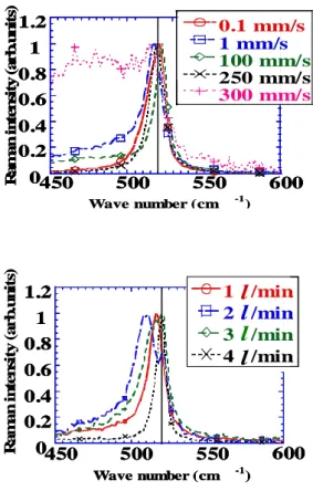
Figure 1 shows Raman spectra of
5000-Å-thick recrystallized Si films annealed
at different v
subs and Fr(Ar)s. The Si layer was
damaged and physically sputtered rapidly,
resulting in a hole being formed quickly
underneath the tube electrode when the v
sub2 was below ~0.1 mm/s. Notably, the Raman peak at 518-520.5 cm
-1corresponding to the c-Si transverse optical (TO) phonon mode was clearly observed for v
subof 0.01-250 mm/s within a 700 μm radius of the tube electrode, and the 100 μm area outside this zone was composed of a mixture of amorphous and crystalline Si. In addition, a symmetrical Raman peak at 518 cm
-1was observed at Fr(Ar) of 4-10 l/min. Thus, highly crystallized poly-Si films were formed by adjusting rf power and Fr(Ar) utilizing the rf microplasma jet at atmospheric pressure.
Fig. 1 Raman spectra of Si films after the plasma annealing at different vsubs and Fr(Ar)s.
The plasma annealing was also performed
in P and B doped a-Si films at P
rf; 30 W, v
sub;1 mm/s and Fr(Ar);1 l/min. Electrical conductivity
σ and its activation energy ΔEσdetermined from the temperature dependence of σ are also shown in Fig. 2 for corresponding n- and p-type a-Si samples before and after the Ar plasma annealing. The
σ increased up to 103S/cm after the plasma annealing, which were two or three orders of magnitudes higher than that of intrinsic poly-Si. As a consequent, both highly crystallized Si(P) and Si(B) films with higher electrical conductivities of 10
1-3S/cm were fabricated by adjusting the v
suband Fr(Ar).
Figure 3 shows Raman spectra of recrystallized a-SiGe
0.6and a-SiOH films at different Fr(Ar)s. Three peaks attributed to Ge-Ge, Si-Ge and Si-Si phonon modes were clearly observed in a-SiGe
0.6at 300, 400 and 500 cm
-1after the plasma annealing. The Raman peak at 518 cm
-1corresponding to the c-Si was also promoted for a-SiOH. The crystallization was observed in the wide plasma conditions compared to that of a-Si, suggesting that the fine structure of the precursor also depend on the degree of the film crystallinity. The rapid recrystallization of a-Si related materials was realized by adjusting the v
suband Fr(Ar).
To understand the recrystallization process of a-Si, the time evolution of the optical reflectivity were monitored using a He-Ne laser (λ=6328 Å) as a function of rf power during the Ar plasma exposure of 50 ms. The rise time and the saturated intensity of optical reflectivity corresponding to the
Wave number (cm -1)
Raman intensity (arb.units)
0 0.2 0.4 0.6 0.8 1 1.2
450 500 550 600
0.1 mm/s 1 mm/s 100 mm/s
250 mm/s
300 mm/sWave number (cm -1)
Raman intensity (arb.units)
0 0.2 0.4 0.6 0.8 1 1.2
450 500 550 600
0.1 mm/s 1 mm/s 100 mm/s
250 mm/s
300 mm/sRaman intensity (arb.units)
0 0.2 0.4 0.6 0.8 1 1.2
450 500 550 600
0.1 mm/s 1 mm/s 100 mm/s
250 mm/s
300 mm/s 0.1 mm/s 1 mm/s 100 mm/s250 mm/s
300 mm/sWave number (cm -1)
0 0.2 0.4 0.6 0.8 1 1.2
450 500 550 600
1 /min 2 /min 3 /min 4 /min
l l l l
Raman intensity (arb.units)
Wave number (cm -1)
0 0.2 0.4 0.6 0.8 1 1.2
450 500 550 600
1 /min 2 /min 3 /min 4 /min
l l l l
Wave number (cm -1)
0 0.2 0.4 0.6 0.8 1 1.2
450 500 550 600
1 /min 2 /min 3 /min 4 /min
l l l l
Raman intensity (arb.units)
3 changes of optical reflective index and temperature of a-Si depend on rf power and Fr(Ar). The optical reflectivity increased with time during 50 ms at P
rfbelow 20 W. It rapidly increased during 10-15 ms and tended to saturate at P
rfover 20 W. Low Fr(Ar) of 1-2
l/min also shorten the rise time and showshigher intensity of the optical reflectivity because the plasma temperature was higher.
In addition, the real time SE study of the recrystallization of a-Si by the plasma annealing revealed that the fine structures at 3.4 and 4.3 eV attributed to the E
1and E
2optical band transitions, respectively, of c-Si band structure were observed after the 15 ms when the rf plasma was turned on, suggesting that the solid-phase crystallization (SPC) occurred. These results suggest that the SPC proceeds quickly after 10-15 ms during the plasma exposure.
B
2H
6/SiH
4PH
3/SiH
4Fig. 2 Electrical conductivities and its activation energy of a-Si(P,B) films before and after plasma annealing.
Fig. 3 Raman spectra of SiGe and SiOH films after plasma annealing at different Fr(Ar)s.
4. DISCUSSION
In addition to the rapid recrystallization of a-Si, the impurity activations of P and B were also promoted as shown in Fig. 2, although the Raman crystallinity of a-Si(B) films was deteriorated rather than the intrinsic a-Si and a-Si(P).The rapid recrystallization of a-Si and its related alloys, a-SiGe, and a-SiOH were performed utilizing the rf plasma jet of argon by adjusting the P
rf,
vsub, and Fr(Ar) (Figs.
1and 3). These suggest that the fine structure of a-Si network used for the precursor also influences the degrees of the film crystallinity.
In fact, the a-SiOH and a-SiGe films were
0 50 100 150 200 250
100 200 300 400 500 600
a-SiGe
0.6 SiGe1l/min2l/min 3l/min 4l/min 5l/min
Wave number (cm-1) Si-Si Si-Ge
Ge-Ge
0 50 100 150 200 250
100 200 300 400 500 600
a-SiGe
0.6 SiGe1l/min2l/min 3l/min
0 50 100 150 200 250
100 200 300 400 500 600
a-SiGe
0.6 SiGe1l/min2l/min 3l/min 4l/min 5l/min
Wave number (cm-1) Si-Si Si-Ge
Ge-Ge
⊿E(eV)Conductivity(S cm-1)
プラズマ照射前
5000 10
4(ppm) (ppm)
10-11 10-9 10-7 10-5 0.001 0.1
10
5000 104
0 0.5 1
After plasma annealing
⊿E(eV)Conductivity(S cm-1)
プラズマ照射前
5000 10
4(ppm) (ppm)
10-11 10-9 10-7 10-5 0.001 0.1
10
5000 104
0 0.5 1
0 0.5 1
After plasma annealing
0 50 100 150 200
100 200 300 400 500 600
a-SiOH
SiOH 1l/min 2l/min 3l/min 4l/min 5l/min
Wave number (cm -1) 0
50 100 150 200
100 200 300 400 500 600
a-SiOH
SiOH
0 50 100 150 200
100 200 300 400 500 600
a-SiOH
SiOH 1l/min 2l/min 3l/min 4l/min 5l/min
Wave number (cm -1)