Surface nanostructure formation and optical properties of black silicon
obtained with He plasma exposure
ヘリウムプラズマ照射によって得られた黒色シリコンの表面ナノ構造形成と光学特性
髙村 秀一✝,青田 達也✝ ✝,岩田 博之✝,前中 志郎✝ ✝,藤田 和宜✝ ✝,玉城 陽平✝ ✝ ✝,
菊池 祐介✝ ✝ ✝,上杉 喜彦✝ ✝ ✝ ✝
Shuichi TAKAMURA✝, Tatsuya AOTA✝ ✝,Hiroyuki IWATA✝, Shiro MAENAKA✝ ✝,
Kazunobu FIJITA✝ ✝, Yohei TAMAKI✝ ✝ ✝, Yusuke KIKUCHI✝ ✝ ✝, Yoshihiko UESUGI✝ ✝ ✝ ✝
Abstract Black silicon formed by helium plasma exposure has attractive surface morphologies in terms of solar cell fabrication since it has a good photon
absorption property over the solar spectrum and does not need any masking process usually employed for the fabrication of pyramid-like microstructures. It would have potential not only for solar cell applications, but also in the fields of photonics, optics, and ultrasonic wave generation. Here, the nano-cone structure formation process, detailed observations of surface morphologies with TEM, the most appropriate He irradiation condition, diffuse reflectance over UV-visible-NIR wavelength, and scattered light enhancement with Raman spectroscopy were studied.
1. Introduction
Black silicon (Si) is an attractive concept in terms of photon capture and trapping in solar-cells,1-11) and
potential for photonic applications12) and terahertz
emission.13) In our previous rapid communication,1)
we have demonstrated the formation of a nano-cone array on Si surfaces with a very simple and mild process of low-energy helium (He) plasma exposure. In reference 9, reactive ion etching (RIE) has been employed with many complicated processes using chemical compounds and inert gases. RIE involves very high energy levels of chlorine, fluorine, or oxygen ion species, hundreds of eV due to a strong radio frequency (RF) biasing, that may damage the † Aichi Institute of Technology, Toyota 470-0392 †† YUMEX Inc., Himeji 671-2114
††† University of Hyogo, Himeji 671-2280 †††† Kanazawa University, Kanazawa 920-1192
surface layer.9,14-16) The neutral beam etching
technology overcomes the damages encountered during RIE, however, the system becomes complicated.17) The present technique employs the
kinetic energy of light noble gas ions (He+) of ≲ 50
eV, an order of magnitude less than the energy for simple RIE, without using any masks.1) It is noted
that a similar needle-type nanostructure has been fabricated by a special plasma etching technique.18)
Fiber-form nanostructures on metal surfaces formed with an irradiation temperature range of 30 to 50 % of the melting point have been recently identified, especially on tungsten (W) material surfaces.19,20) The so-called fuzzy W surface is black;
thus not only the spectral emissivity over a wide light wavelength but also the total emissivity for a wide temperature range is very close to 1.0, yielding a complete black-body.21) The physical mechanism for
investigated in terms of He bubble and/or cluster formation in nanofibers as well as ground surfaces, and its effect on mechanical properties, such as shear modulus22,23) has been studied. In reference 24, it is
suggested that the He effect on non-metal materials such as Si should be examined.
In this work, the formation mechanism of nano-cone array structure and surface morphologies were investigated by detailed FE-SEM and TEM observations. Furthermore, the He irradiation condition was optimized, and diffuse reflectance over a wide wavelength of light, and scattered light enhancement with Raman spectroscopy were studied.
2. Formation Processes and Surface Morphology 2.1. Nano-cone array formation processes
He plasma has a curious effect on metal surfaces, especially refractory metals, such as W and molybdenum (Mo), in relation to fusion energy research development since He is a product of fusion reaction, and W is a candidate material for plasma-facing components owing to its high melting point. Since the discovery of fiber-form nanostructures on W surfaces,19,20) a number of works have been carried out
because the fuzzy morphology has hitherto unseen interesting properties. Material scientists have investigated the formation process theoretically22,23,25)
and computationally.26) Nevertheless, the precise
mechanism is currently a hot topic, and experimentally, its application to non-metal materials, such as Si24) is
interesting.
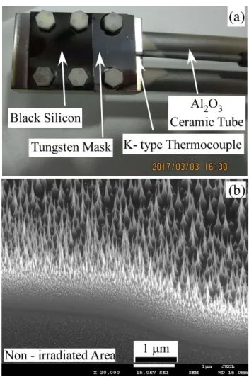
Figure 1 shows a typical black Si formation process. As shown in Fig. 1(a), a part of Si surface put on a cooled stage was covered with a W mask in this case for the flux gradient method24,27,28) to clarify the
nano-cone array formation mechanism. We choose a p-type Si wafer with a low resistivity (Nilaco: SI500440, mirror index 100) because we may apply external voltage on the Si specimen to control the He ion impinging energy. A clean plasma-facing surface Si ensures a uniform He ion flux on it. An increase in the surface temperature, usually more than 500°C makes Si substrate electrically conductive because the carrier
density increases as the temperature increases due to intrinsic transition. The substrate was irradiated by a high-density He plasma in a compact plasma device AIT- PID.29)
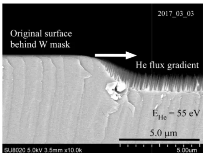
Figure 1(b) is an FE-SEM image with a grazing view at the mask edge region. The lower part of image indicates non-irradiated area, while the upper part corresponds to He-plasma-irradiated surface. Across this boundary, the He ion flux has a gradient, the so-called flux gradient irradiation, which makes the transformation of time evolution to spatial variation. Figure 2 shows an FE-SEM image of CP cross section
Fig. 1. Black silicon formation. (a) black silicon formed on water-cooled sample stage (40×24 mm in surface area) made of stainless-steel. A part of Si surface was covered with a tungsten mask. K-type thermocouple was inserted between Si wafer (30×24×0.5 mm) and electrically insulated artificial mica. (b) Grazing view of boundary layer between irradiated and non-irradiated area of black Si for “flux gradient method” with FE-SEM. He ion flux He = 1.7×10²¹ m-2s-1, fluence He = 1.3×1025 m-2, and the surface temperature of T = 500 °C.
of the image shown in Fig. 1(b). We can clearly distinguish an original Si surface just below the W mask, a transient region, and a main irradiation zone. In this case, the He ion impinged on the Si surface is sufficiently high, at 55 eV, corresponding to a Si sputtering yield of 0.006. The base height of nano-cone array area is lower than that of the original Si surface by two microns, while the tips of the nano-cone array have a height of one micron below the original surface. We noted that He ion energy is much lower than the threshold energy for W, thus, we did not consider W contamination on Si surface. These observations suggest erosion to be the formation process. The so-called Bradley & Harper (BH) instability30) and
incident angle dependence of sputtering yield would play a role in the formation of such a needle-cone type surface morphology; that is, the negative curvature of surface height may produce slower erosion, while the positive curvature may bring faster erosion.
On the other hand, in the initial incubating stage or in the case of a low-energy He ion incidence, the He clusters and bubbles may contribute to determining the initial spatial density of nano-cones, as discussed in reference 1. Many point areas containing He bubbles or clusters may serve as formation precursors that have some resistance against physical sputtering. In this irradiation experiment, the He ion fluence, He =
1.3×1025 m-2, and the sputtering yield of Si at the He
ion energy of 55 eV is 0.006 so that the fluence of sputtered Si atoms, Si = 7.8×10²² m-2. Si crystal has a
diamond structure in which eight Si atoms form a unit cell. Therefore, the number density of Si atoms is nSi =
8/a3 = 5.0×1028 m-3, where the lattice constant a is
0.543 nm. Thus, the erosion depth of Si is estimated to be Si /nSi = 1.6×10⁻⁶ m = 1.6 m. This value is
reasonable compared to the experimental observation shown in Fig. 2.
We could not detect any sputtering-resistant heavy metals such as W and Mo, but only carbon with EDX measurement. Carbon has almost the same as or weaker sputtering yield than that of Si. Therefore, we can say that sputter-resistant heavy metals are not the origins of cone formation.
2.2 TEM observations of nano-cones
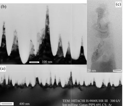
Figure 3 shows the TEM bright field images of nano-cones on the surface of black Si with different magnifications. Figure 3(c) shows a magnified view of the nano-cone tip, which shows a complicated structure in the cone tip region.
In order to clarify the nano-cone structure, the bright field image (left) and dark field one (right) are compared in Fig. 4. The dark field image shows stripe pattern in the base bulk Si, with half the nano-cones connecting with bulk Si. On the other hand, the top half of nano-cone is dark, which indicates a different structure from that of the Si crystal. Figure 5 shows more clear crystal structure with some dislocations, as indicated by arrows, which are probably thermally induced defects. The electron diffraction pattern shown in Fig. 5(b) was obtained in the direction of electron beam along the zone axis for the {110} surface of Si wafer and confirms a good crystalline structure.
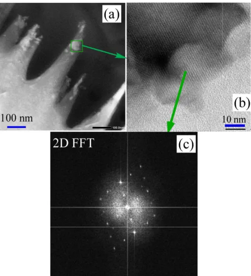
Figures 6 (a) and (b) show the local TEM images, which reveal the presence of nano-crystals at the cone tip. The 2-D FFT image shown in Fig.6(c) reveals crystalline nature. Figure 7 shows the side structure at the middle of the nano-cone with different magnifications, demonstrating the presence of nano-crystals. These nano-crystals do not have the
Fig. 2. FE-SEM image showing a CP (Cross sectional Polisher) made cross section of black Si boundary layer. The left-hand side corresponds to non-irradiated region, while the right-hand side does He plasma irradiated one. The irradiation is the same as in Fig. 1.
same crystal orientation. Nao-beam diffraction also show some Laue spots indicating crystalline structure. To study more on the morphology of cone tip region, EBSD (Electron Back Scattering Diffraction) would also be a useful tool for further investigations discriminating crystallinity.
3. Optimization of He Irradiation Condition for obtaining Black Si
We obtained several grades of “black Si.” It is quite helpful to identify the condition for obtaining a “good” black Si, where “good” will become clear later in this section. Photographic comparison of several grades of Fig. 3. TEM bright field images of black Si with different magnifications among (a) ~ (c).
He = 2.0×10²¹ m-2s-1, He = 2.0×1025 m-2, EHe = 40 eV, T = 650°C.
Fig. 4. Comparison between bright-field image (left) and dark-field one (right) in TEM observation. Arrows show thermally induced defects (dislocations). The irradiation condition is the same as that in Fig. 3.
.
Fig. 5. TEM observation with weak beam dark field image (a) and Laue diffraction pattern (b). Arrows show dislocation defects probably induced thermally.
Weak Beam Dark Field Image
2 nm-1
200 nm Electron Diffraction Pattern
Direction of electron beam is along zone axis for {110} crystal surface of Si wafer
(a)
(b)
Fig. 6. Nanocrystals on cone tips. (a) nanocrystals on the middle side of nano-cone, (b) magnified TEM view showing regular lattice of Si crystal, (c) two-dimensional FFT of the image (b), showing crystal component.
black Si is made in Fig. 8, where (a) shows the surface with weak He plasma irradiation, (b) seems to be the best surface, and (c) corresponds to an excess exposure to He plasma and its color is whitish blue. Each irradiation condition is summarized in the figure caption. The He ion fluence multiplied by sputtering yield determined by He ion incident energy gives the apparent sputtered Si atom density, that is, (a) 2.2×10²²
atoms/m2, (b) 8.1×10²² atoms/m2, and (c) 16×1022
atoms/m2. Here, we did not consider re-deposition and
angle dependence of He ions. The surface morphologies responsible for the above differences is explained below. FE-SEM images of good black Si and whitish blue Si are shown in Figs. 9(a) and (b), respectively. In
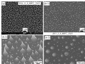
Fig. 9(a), the apparent radius of the white cone is relatively small and uniform, and it does not contain big one, while the whitish blue Si shown in Fig. 9(b) has a broad range of radii. Quantitative evaluation for this difference is shown in Fig .10, where the nano-cone thickness is plotted as a function of diameter in pixel for the good black Si (Fig. 9(a)) and whitish blue Si (Figs. 9(b)). The former shows a significant decrease in the number of large-diameter cones, while the latter exhibits a broad distribution for large-diameter cones. This is apparent from Figs. 9(b-1) ~ (b-3).
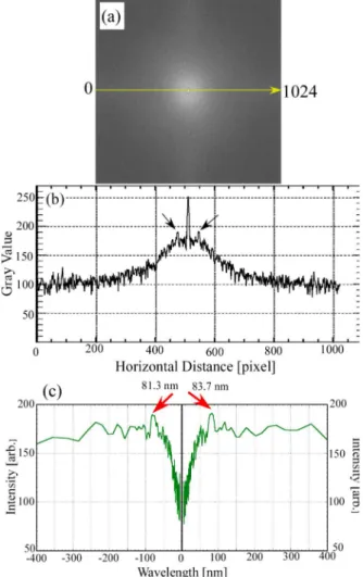
Two-dimensional digital Fourier analysis of nano-cone locations on the black Si surface using Image J code31) was applied for a square top view
FE-SEM image similar to Fig. 9(a) but with slightly less He plasma exposure with the scale of bitmap format composed of 1024×1024 elements. For this analysis, a circular window function was employed, and the 2-D spectrum thus obtained is shown in Fig. 11(a). One-dimensional profile by cutting the central peak is shown in Fig. 11(b), demonstrating side-band peaks, which appear 34.5 pixel apart from the central peak, and corresponds to 82.6 nm in length. The wavelength spectrum was obtained by transforming from Fig. 7. Nanocrystals on the side of nano-cone tip. (a)
Nano-cones TEM image, (b) enlarged view of the tip side of nano-cone, (c) TEM observation with a maximum magnification, showing local crystal regularity.
100 nm (a) 20.0 nm 10.0 nm (c) (b)
Fig. 8. Photographic comparison among several black silicons. (a) weak exposure to He plasma: EHe = 35 eV, T = 500 °C, He = 1.2×10²¹ m-2s-1, He =0.88×1025 m-2, (b) good exposure: EHe = 45 eV, T = 700 °C, He = 1.8×10²¹ m-2s-1, He =1.3×1025 m-2, (c) excessive exposure: EHe = 55 eV, T = 600 °C, He = 2.2×10²¹ m-2s-1, He =1.6×1025 m-2.
Fig. 9. SEM comparison between Si with good and excessive exposure of He plasma. (a) good black Si: EHe = 55 eV, T = 607 °C, He = 1.3×10²¹ m-2s-1, He =0.94×1025 m-2. (b) bluish Si: the formation condition is the same as in Fig8(c). (b-1) and (b-2) show top views with different magnifications, and (b-3) shows a grazing view.
wavenumber one, as shown in Fig. 11(c), where the sideband peak appears at 80~85 nm, corresponding to the average distance between the neighboring nano-cones. Several window functions with different circle radii yielded similar values for the sideband peaks.
Further, we observed some patterns or a kind of regularity in the nano-cone array. Since 2-D FFT is not appropriate for such topological characteristics, a kind of fractal analysis is required, which is open to further evaluation in near future. Some nano-cones lie on a straight or curved line, similar to a mountain ridge, which could reflect crystal orientation. Figure 12 shows the effect of irradiation conditions on surface morphology, focusing on the effect of He ion energy and He ion fluence on the p-Si wafer. As discussed in Fig. 8, we compared the apparent Si erosion, that is, the product of He ion fluence and sputtering yield determined by incident He ion energy: (a) Si
=2.2×10²² atoms/m2 corresponds to weak exposure, (b)
Si = 7.8×10²² m-2 corresponds to a slightly low erosion
compared to the best black Si, (c) Si = 7.1×10²² m-2
indicates good black Si formation, and (d) Si =
18×1022 m-2 indicates whitish blue Si formation.
4. Optical Properties of Black Si
Fig. 10. Nano-cone thickness distribution as a function of diameter in pixcel for black (Fig.9(a)) and bluish-white (Fig.9(b)) silicons
Fig. 11. Two-dimensional Fourier analysis of nano-cone locations on black Si with slightly insufficient exposure using Image J. (a) 2D wavenumber spectrum, (b) Inverse wavelength spectrum, (c) wavelength spectrum obtained from (b). The irradiation condition is as follows: EHe = 40 eV, T = 500 °C, He = 1.4×10²¹ m-2s-1, He = 1.0×1025 m-2. 2017_05_20 500C, 35 eV 100 nm (a) 2017_05_25 700C, 40 eV 100 nm (b) 2017_05_26 700C, 45 eV 100 nm (c) (d) 600C, 55 eV 2017_03_04 100 nm
Fig. 12. Effect of irradiation condition on surface morphology, focusing on He ion energy and surface temperature. (a) corresponds to Fig. 8(a), (b) EHe = 40 eV, T = 700 °C, He = 2.3×10²¹ m-2s-1, He =1.7×1025 m-2. (c) corresponding to Fig. 8(b), (d) to Fig. 9(b).
Raman spectroscopy (JASCO NRS-2100) provides information on inter-atomic coupling, crystallinity, and internal stress. Figure 13 shows the Raman spectra with an incident laser wavelength of 514.5 nm on He-plasma-treated Si (colored lines) as well as pristine p-Si wafer (black line) in the wavenumber range of 480 - 560 cm-1. The spectra show sharp peaks at 520 cm-1
that corresponds to a diamond cubic Si crystal. B-Si a (green line) represents ideal black Si, B-Si b (purple line) represents black Si with slightly lower He plasma exposure, B-Si c (blue line) represents whitish blue Si, and B-Si d represents another good black Si. The scattered light is located at 520 cm-1, with a modest
shift from that of pristine Si. This implies that the residual stress would be small. The FWHM of each profile is indicated in parenthesis in the figure, and is not large compared to that of the pristine one. Even the broadest one (B-Si d) is 16 % compared to that of the pristine one; this substrate was not placed on the cooling stage for He plasma exposure, but suspended by an R-type thermocouple with a sheath diameter of 0.5 mm.
Although the thermocouple showed 600 °C, the highest temperature region caused by He plasma exposure was away from the location of thermocouple, and thus, the temperature there would be much higher than the value obtained with the R-type thermocouple.
This may be the reason for the relatively large FWHM. Thermally induced dislocations observed through TEM (see Fig. 5), would affect the degree of crystallinity. In addition, the fact that the top half of nano-cone does not consist of single crystals would affect the overall crystallinity. Good black Si exhibits scattering enhancement by more than a factor of 5, which suggests a fairly good photon trapping ability.
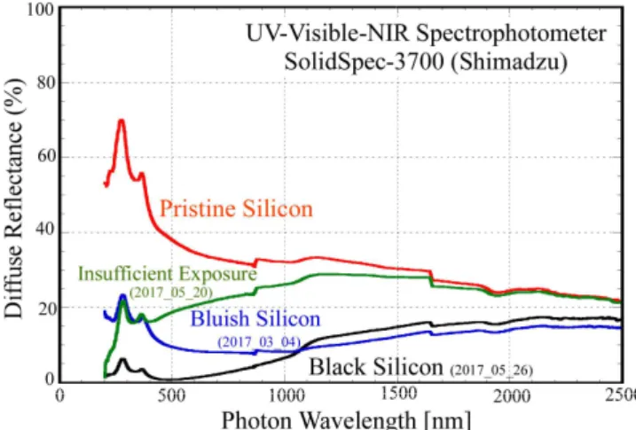
Amplification of Raman scattered light intensity is represented in Fig. 13, and the surface morphology discussed in Section 2 is appropriate for incident photon capturing and trapping, which influences the light reflectivity of black Si. Incident photons on Si nano-cone array surface are partially absorbed and partly reflected. The photons reflected on the cone surfaces can be absorbed at a neighboring nano-cone surface. These processes enhance photon capture and trapping in the nano-sized Si cone array. Figure 14 shows the comparison among diffuse reflectances over a wide ultraviolet (UV) – visible – near infrared (NIR) wavelength range, between 200 and 2500 nm (Shimadzu SolidSpec – 3700). The red line represents that for pristine p-Si wafer, whereas the blue one corresponds to the whitish blue Si corresponding to Fig. 9(b) and the green one does to insufficiently exposed Si corresponding to Fig. 8(a). A substantial reduction in diffuse reflectance was Fig. 13. Raman spectra for various kinds of Si under different
conditions. B-Si a: Fig. 8(b); B-Si b: slightly low exposure Fig. 12(c); B-Si c: whitish blue Si similar to Fig. 8(c); B-Si d: good black Si in Fig. 9(a).
Fig. 14. Diffuse reflectance of several kinds of black Si as a function of photon wavelength over UV-visible-NIR range. Black Si is the same as that under the condition in Fig. 8(b).
noted for the good black Si at least between 200 and 1000 nm, which is an important wavelength range for solar cell applications although the reduction is not sufficient compared to the nanostructured surface obtained with a special etching technique.32) As a
reference, the diffuse reflectance of a well-grown W fuzz surface has already been reported in references 1 and 21, showing a very small reflectance over a wide wavelength range. Insufficiently exposed Si does not absorb well over a global wavelength range. However, we note that it has a substantial absorption at about 200 ~ 250 nm (see the green line in Fig. 14). This is possibly because the average distance between the neighboring nano-cones is shorter (see Fig. 12(a)) than that in the heavily exposed Si surface (see Figs. 12(b) ~ (d)), and thus, the UV photons with small wavelengths could be trapped and absorbed.
5. Summary and Conclusions
The present study on black Si formation, surface morphology, and optical properties demonstrated a novel process to obtain nanostructures on Si surfaces for potential application in optical and/or photonic devices. The present technique employed no mask and involved fewer processes favoring industrial utilization. Moreover, the process circumvents the use of masks, etching liquids, and chemical gases, and involves soft ion bombardment to Si crystal because the incident He ions have a lower kinetic energy compared to that used in standard RIE for obtaining microscopic textures on Si surfaces to reduce reflectivity. The present technique provides a simple tool with reduced damages on Si crystal.
The formation mechanism of dense Si nano-cone array of black Si was investigated with respect to growth or erosion using the flux gradient method. The current understanding of formation mechanism has been discussed in terms of sputtering process. The role of surface temperature is not clear at the moment. However, at the initial stage, a kind of growth process serving as a precursor cannot be excluded and is open to further investigation. On the other hand, there would
be a possibility of impurity contribution for the same initial precursor formation or incubating phase.
A comparison between dark and bright field TEM images indicated that the base of the cone tip was crystalline with some thermally induced dislocations, while the tip was amorphous or comprised an aggregation of nano crystals. This may be related to precursor formation.
Further, the optimal He plasma irradiation condition for the formation of good black Si was qualitatively identified with image analysis technique. The desirable product of He ion fluence on Si surface and physical sputtering yield determined by incident He ion energy, that is, the apparent sputtered Si atom density was 8×10²² Si atoms/m2. If the sputtered atom density
exceeds this value substantially by employing a high He ion fluence or high He ion energy, then the surface becomes whitish blue. On the other hand, weak exposure yielded a light brown surface. We should note that impurity species such as oxygen would contribute to the real sputtering yield in the low-energy range of He+ ions. The threshold energy is 20 eV for pure He+
ions incident on the Si surface.
FE-SEM image analysis revealed the surface morphology for an ideal black Si, which has a dense nano-cone array with uniform height on the Si wafer. This is qualitatively demonstrated by the diagram showing the distribution of nano-cone thickness in the SEM image with the use of standard image analysis. Whitish blue Si has a broad distribution of nano-cone thickness, especially in the large thickness range. Raman spectroscopy showed a substantial amplification in the scattered intensities, which is over five times as large as that of pristine Si, and a modest change in peak position and FWHM. Black Si showed the lowest diffuse reflectance among the several grade of He-irradiated samples. The reflectance of a good black Si is 10 % over 200 ~ 1000nm, which is suitable for solar cell application. Weakly exposed Si has a small reflectance at 200 ~ 250 nm UV range, probably due to the small height of nano-cone and the short average distance between the neighboring nano-cones. This suggests a potential for UV photonics.
Acknowledgments
One of the authors (S.T.) acknowledges Professor H. Saka of AIT for his advice to TEM images, H. Morooka of TDK corporation for his discussions on solar cell, and K. Yamada of YUMEX Inc. for his efforts of surface evaluation of black Si.
References
1) S. Takamura, Y. Kikuchi, K. Yamada, S. Maenaka, K. Fujita and Y. Uesugi, “Nanostructure formation on silicon surfaces by using low energy helium plasma exposure”, Jpn. J. Appl. Phy. 55, 12301 (4 pages) (2016). 2) M. Kanechika, N. Sugimoto, and Y. Mitsushima,
“Control of shape of silicon needles fabricated by highly selective anisotropic dry etching”, J. Vac. Sci. Technol. B 20, 1298-1302 (2002).
3) J. Oh, H.-C. Yuan, and H.M. Branz, “An 18.2%-efficient black-silicon solar cell achieved through control of carrier recombination in nanostructures”, Nature Nanotech. 7, 743 (6 pages) (2012).
4) X. Ao, X. Tong, D.S. Kim, L. Zhang, M. Knez, F. Müller, S. He, and V. Schmidt, “Black silicon with controllable macropore array for enhanced photoelectrochemical performance”, Appl. Phys. Letters 101, 111901 (4 pages) (2012).
5) Y. Matsui and S. Adachi, “Optical properties of “black silicon” formed by catalytic etching of Au/Si(1000) wafers”, J. Appl. Phys. 113, 173502 (9 pages) (2013). 6) H.Y. Chen, G.D. Yuan, Y. Peng, M. Hong, Y.B. Zhang,
Z.Q. Liu, J.X. Wang, B. Cai, Y.M. Zhu, and J.M. Li, “Enhanced performance of solar cells with optimized surface recombination and efficient photon capturing via anisotropic-etching of black silicon”, Appl. Phys Letters 104, 193904 (4 pages) (2014).
7) M. Hong, G.D. Yuan, Y. Peng, H.Y. Chen, Y. Zhang, Z.Q. Liu, J.X. Wang, B. Cai, Y.M. Zhu, Y. Chen, J.H. Liu, and J.H. Li, “Control carrier recombination of multi-scale textured black silicon surface for high performance solar cells”, Appl. Phys. Letters 104, 253902 (5 pages) (2014). 8) H. Savin, P. Pepo, G. Gastrow, P. Ortega, E. Calle, M. Garin, and R. Alcubilla, “Black silicon solar cells with integrated back-contacts achieve 22.1% efficiency”, Nat. Nanotechnol 10, 624 (6 pages) (2015).
9) P. Ortega, E. alle, G. von Gastrow, P. Repo, D. Carrio, H. Savin and R. Alcubilla, “High-efficiency black silicon interdigitated back contacted solar cells on p-type and n-type c-Si substrates”, Prog. Photovolt: Res. Appl. 23, 1448-1457 (2015).
10) H.-C. Yuan, V.E. Yost, M.R. Page, P. Stradins, D.L. Meier, and H.M. Branz, “Efficient black silicon solar cell with a density-graded nanoporous surface: Optical properties, performance limitations, and design rules”, Appl. Phys. Lett. 95, 123501 (3 pages) (2009).
11) K. Imamura, D. Irishika and H. Kobayashi, “Surface nanocrystalline Si structure and its surface passivation for highly efficient black Si solar cell”, Prog. Photovolt: Res. Appl. 25, 358-366 (2017).
12) Y. Tanaka, K. Ishizuka, M.De Zoysa, T. Umeda, Y. Kawamoto, S. Fujita and S. Noda, “Photonic crystal microcrystalline silicon solar cells”, Prog. Photovolt: Res. Appl. 23, 1475-1483 (2015).
13) P. Hoyer, M. Theuer, R. Beigong, and E.-B. Kley, “Terahertz emission from black silicon”, Appl. Phys. Letters 93, 091106 (3 pages) (2008).
14) H. Wada, M.Agata, K. Eriguchi, A. Fujimoto, T. Kanashima, and M. Okayama, “Photoreflectance characterization of the plasma-induced damage in Si substrate”, J. Appl. Phys. 88, 2336 -2341 (2000). 15) M. Steglich, T. Käsebier, M. Zilk, T. Pertsch, E.-B. Kley,
ans A. Tünnermann, “The structural and optical properties of black silicon by inductiveluy coupled plasma reactive ion etching”, J. Appl. Phys. 116, 173503 (12 pages) (2014).
16) X. Liu, P.R. Coxon, M. Peters, B. Hoex, J.M. Cole, and D. Fray, “Blacj silicon: fabrication methods, properties and solar energy applications”, Energy Environ. Sci. 7, 3223-3263 (2014).
17) S. Samukawa, “Ultimate Top-down Etching processes for Future Nanoscale Devices: Advanced Neutral-Beam Etching”, Jpn. J. Appl. Phys. 45 2395-2407 (2006). 18) A. Hatta, “Microscopic Silicon Needles Fabricated by
Plasma Etching”, pp.717-728, in Controlled Nanofabrications: Advances and Applications, ed. By Liu Ru-Shi, Pan Stanford publishing Pte. Ltd., Singapore 2012.
19) S. Takamura, N. Ohno, Dai Nishijima, and S. Kajita, “Formation of Nanostructured Tungsten with Arborescent Shape due to Helium Plasma Irradiation”, Plasma Fusion Res. 1, 051 (2 pages) (2006).
20) M.J. Baldwin, D.P. Doerner, “Helium induced nanoscopic morphology on tungsten under fusion relevant plasma conditions”, Nucl. Fusion 48, 035001 (5 pages) (2008).
21) S. Takamura, “Radiative cooling properties of he-defected tungsten with fiber-form nanostructured surface”, J. Nucl. Mater. 466, 239-242 (2015).
22) R.D. Smirnov, S.I. Krasheninnikov and J. Guterl, “Atomistic modeling of growth and coalescence of helium nano-bubbles in tungsten”, J. Nucl. Mater. 463, 358-362 (2015).
23) S.I. Krasheninnikov and R.D. Smirnov, “He cluster dynamics in fusion related plasma facing materials”, Nucl. Fusion 55, 073005 (2015).
24) S. Takamura, and Y. Uesugi, “Experimental identification for physical mechanism of fiber-form nanostructure growth on metal surfaces with helium plasma irradiation”, Appl. Surf. Sci. 356, 888 (2015).
fuzz growth”, Phys. Scr. T145 014040 (4 pages) (2011). 26) A.M. Ito, A. Takayama, Y. Oda, T. Tamura, K.
Kobayashi, et al., “Molecular dynamics and Monte Carlo hybrid simulation for fuzzy tungsten nanostructure formation”, Nucl. Fusion 55, 073013 (11 pages) (2015). 27) S. Takamura, “Initial Stage of Fiber-Form Nanostructure
Growth on Refractory Metal Surfaces with Helium Plasma Irradiation”, Plasma Fusion Res. 9, 1302007 (3 pages) (2014).
28) G. Kawamura, N. Ohno, S. Takamura and Y. Tomita, “A Particle-In-Cell approach to particle flux shaping with a surface mask”, Nucl. Mater. Energy 12, 297-301 (2017).
29) S. Takamura, “Characteristics of the Compact Plasma Device AIT-PID with Multicusp Magnetic Confinement”, IEEJ Trans. 7(S1), S19 (2012).
30) W.L. Chan and E. Chanson, “Making waves: Kinetic processes controlling surface evolution during low energy ion sputtering”, J. Appl. Phys. 101, 121301 (46 pages) (2007).
31) https://imagej.nih.gov/ij/
32) H.M. Branz, V.E. Yost, S. Ward, K.M. Jones, B. To, and P. Stradins, “Nanostructured black silicon and the optical reflectance of graded-density surfaces”, Appl. Phys. Letters 94, 231121 (3 pages) (2009).