INVITED PAPER
Special Section on Recent Advances in Ultra-high-speed Photonic Devices for Next-generation Optical Fiber CommunicationsHigh-Speed EA-DFB Laser for 40-G and 100-Gbps
Shigeki MAKINO†a), Kazunori SHINODA†, Members, Takeshi KITATANI†, Nonmember, Hiroaki HAYASHI†, Member, Takashi SHIOTA†, Shigehisa TANAKA†, Nonmembers, Masahiro AOKI†, Member, Noriko SASADA††, Nonmember, and Kazuhiko NAOE††, Member
SUMMARY We have developed a high-speed electroabsorption mod-ulator integrated distributed feedback (EA/DFB) lasers. Transmission per-formance over 10 km was investigated under 25 Gbps and 43 Gbps mod-ulation. In addition, the feasibility of wide temperature range opera-tion was also investigated. An uncooled EA/DFB laser can contribute to the realization of low-power-consumption, small-footprint and cost-effective transceiver module. In this study, we used the temperature-tolerant InGaAlAs materials in an EA modulator. A wide temperature ranged 12 km transmission with over 9.6 dB dynamic extinction ratio was demon-strated under 25 Gbps modulation. A 43 Gbps 10 km transmission was also demonstrated. The laser achieved a clear, opened eye diagram with a dy-namic extinction ratio over 7 dB from 25◦C to 85◦C. The modulated out-put power was more than+2.9 dBm even at 85◦C. These devices are suit-able for next-generation, high-speed network systems, such as 40 Gbps and 100 Gbps Ethernet.
key words: electro absorption modulator, EA, DFB laser, uncooled,
In-GaAlAs, Ethernet, 40 Gbps, 100 Gbps
1. Introduction
An electroabsorption modulator integrated distributed feed-back (EA/DFB) laser has several advantageous features of high speed, low chirp, low power consumption, and com-pactness. 1.55μm range EA/DFB lasers are now mainly used for 10 Gbps intermediate-reach (IR: 40 km), long-reach (LR: 80 km) categories for MAN/WAN applications and 40 Gbps very-short-reach (VSR: 2 km) application. Re-cently, because of the explosive increase of data traffic due to the world wide spread of broadband services, upgrades of network equipment has become essential and the stan-dardization of next generation high speed network, e.g. 100 Gbps and 40 Gbps Ethernet is in progress [1]. The ultra-high-speed 1.3μm range EA/DFB laser is regarded as the promising candidate for the next-generation high-speed net-work standard. A 1.3μm range, 25 Gbps 4 channel wave-length division multiplexing (WDM) scheme is suitable for cost-effective 100 Gbit Ethernet client side technology, and 40 Gbps EA/DFB laser is considered as the cost-effective solution for 40 Gbps Ethernet. Because of the low chirp and small fiber dispersion compared to the 1.55μm range, it can be expected that this device can transmit a high-speed signal
Manuscript received November 12, 2008. Manuscript revised February 23, 2009.
†The authors are with Hitachi, Ltd., Central Research
Labora-tory, Kokubunji-shi, 185-8601 Japan.
††The authors are with Opnext Japan, Inc., Yokohama-shi,
244-8567 Japan.
a) E-mail: [email protected] DOI: 10.1587/transele.E92.C.937
over 10 km single-mode fiber (SMF).
In addition, the power consumption of network equip-ment becomes a critical issue and the reduction of power consumption is one of the most important keys for recent optical devices. For effective power reduction of EA/DFB laser modules, a peltiert device free operation is strongly desired like the case of uncooled directly-modulated laser. However, uncooled operation of EA/DFB lasers has been highly challenging because the devices are very sensitive to the change of operating temperature. That is to say the tem-perature sensitivity of the EA absorption peak wavelength (λEA) is about six or seven times larger than that of the DFB
lasing wavelength (λDFB). This causes a large variation in
the wavelength detuning (the difference between λDFB and
λEA), which is a key parameter that dominates the
modu-lation performances such as extinction ratio, chirping and output power. To overcome this problem, a new voltage off-set method was proposed [2]. By adjusting the bias volt-age of the EA modulator along with temperature variation, the wavelength detuning and the modulation performances could be maintained at almost same level over wide temper-ature range. Some other attempts have also been made to achieve an uncooled EA modulator of EA/DFB laser [3]– [6]. We have investigated an InGaAlAs EA modulator and butt joint integration of optical components and also devel-oped a specialized manufacturing technique. Due to the temperature-tolerant characteristics of InGaAlAs material and monolithic integration of individually optimized opti-cal components, we have achieved 1.55μm range 10 Gbps 40 km and 80 km SMF transmission over wide temperature range [7]–[9].
In this paper, we demonstrated uncooled 1.3μm range 25 Gbps and 40 Gbps EA/DFB lasers as light source for 100 Gbps, 40 Gbps Ethernet 10 km SMF specifications. To achieve the uncooled operation of 1.3μm range EA/DFB laser, we used a temperature-tolerant InGaAlAs EA mod-ulator and butt joint integration technique, as same as a 1.55μm range application. By using these technologies, 25.8 Gbps 12 km SMF transmission over a wide tempera-ture range from 0◦C to 85◦C with over 9.6 dB of dynamic extinction ratio was successfully achieved [10]. In addition, we developed an uncooled 1.3μm range 40 Gbps EA/DFB laser. This laser demonstrated a 43 Gbps 10 km SMF trans-mission over a wide temperature range for the first time [11].
cient extinction ratio and increase of resistance of the EA modulator. Firstly, we designed the undoped layer thickness and modulator length in order to realize the low-RC-time constant, then optimized the multi quantum well (MQW) structure to strike a balance between the high frequency bandwidth and practical modulation performances. In this study, 60 nm thick undoped bulk layer was inserted in be-tween p-InP cladding layer and multi quantum well (MQW) to reduce the junction capacitance in expectation of di ffu-sion of p-type dopant during the fabrication process. In ad-dition, we adopted the low parasitic capacitance structure based 40 Gbps EA/DFB laser.
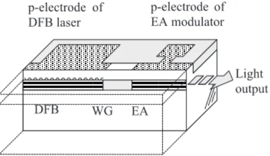
Figure 1 shows the schematic structure of an uncooled EA/DFB laser. The device consists of a 100-μm-long In-GaAlAs EA modulator, a 400-μm-long DFB laser, and a 60-μm-long bridge waveguide (WG) in between. All com-ponents were grown by metalorganic vapor phase epitaxy (MOVPE) and monolithically integrated on an n-InP sub-strate. The temperature-tolerant characteristics of the In-GaAlAs material are based on its advantageous band struc-ture, a larger conduction band offset combined with a smaller valence band offset than the conventional InGaAsP materials [12], [13]. Based on this superior band structure, substantial improvement is expected in the trade-off rela-tionship among extinction ratio, chirp and output power han-dling capability of the EA modulator [14]. In this study, con-duction band offset is set to be over 200 meV in order to re-alize the large extinction ratio over wide temperature range. In addition, the optical confinement factor of EA MQW is designed to be over 30% by adjusting the number and thick-ness of MQW.
The device structure was fabricated using a multistep butt joint etching/regrowth technique [15], [16]. By apply-ing this technique, we could optimize each optical compo-nent independently, and it is essential to realize a practi-cal performance of both EA modulator and DFB laser over
Fig. 1 Schematic structure of EA/DFB laser.
tor.
3. Device Performance
The typical lasing spectra of EA/DFB lasers at 0◦C, 25◦C, 55◦C and 85◦C are shown in Fig. 2. The lasing wavelength is designed to be 1290 nm at 55◦C. Wavelength variation between 0◦C and 85◦C was about 7 nm. Stable single-mode operations with over 40 dB of sub-mode suppression ratio (SMSR) were obtained for all operating temperatures. Fig-ure 3 plots the static extinction ratio (SER) characteristics at 25◦C, 55◦C and 85◦C.
By reflecting the ideal band structure of InGaAlAs ma-terial and carefully optimized quantum-well design, wave-length detuning, and modulator wave-length, we were able to ob-tain over 20 dB SER at−4 V EA bias voltage. Figure 4 plots the E/O response (S21) of uncooled EA/DFB laser at 25◦C.
Over 30 GHz 3-dB frequency bandwidth was observed. The measured total capacitance of EA modulator was 0.18 pF, and it was also estimated that the contribution ratio of para-sitic capacitance was about 50%.
Figure 5 shows non-filtered eye diagrams obtained
un-Fig. 2 Typical lasing spectra of EA/DFB laser.
Fig. 4 E/O response at 25◦C.
Fig. 5 25.8 Gbps eye diagrams before and after 12 km SMF transmission.
der 25.8 Gbps modulation at (a) 0◦C and (b) 85◦C. In this measurement, the device is packaged in a conventional but-terfly module. Modulation amplitude voltage was applied from pulse pattern generator and bias voltage was applied from DC power supply via bias-tee. Proper bias voltage was applied at various operating temperature to obtain al-most 50% of optical cross point and good modulation per-formances. We used a non-return to zero, 231− 1 pseudo-random bit stream. The upper pictures are back-to-back, and the lower pictures are after a 12 km normal SMF transmis-sion. As shown in these pictures, clearly opened eye dia-grams were obtained at all operating conditions. The modu-lation amplitude voltage was below 2.5 V and the maximum bias voltage at 0◦C was−1.5 V. The measured dynamic ex-tinction ratios (DER) were 9.9 dB and 9.6 dB at 0◦C and 85◦C.
The modulation performances at various operating temperatures are plotted in Fig. 6. As shown in this figure, we obtained a high DER of more than 9.6 dB over wide tem-perature range.
Figure 7 shows a non-filtered eye diagram under 43 Gbps modulation at (a) 25◦C and (b) 85◦C. 43 Gbps, non-return to zero, 27 − 1 pseudo-random bit stream was used.
In this measurement, modulation performances were inves-tigated by chip on carrier. Because of the dew condensation at low temperatures, the lowest measurement temperature was limited at 25◦C. The modulation amplitude voltage of 2.2 V was used at all operating temperatures. The upper
pic-Fig. 6 25.8 Gbps modulation performances over wide temperature.
Fig. 7 43 Gbps eye diagrams before and after 10 km SMF transmission.
Fig. 8 43 Gbps modulation performances over wide temperature.
tures represent back-to-back, and lower pictures represent after 10 km SMF transmission. The eye diagrams are clearly open both before and after 10 km transmission.
Figure 8 plots DER and bias voltage at various op-eration temperatures. The DER is over 7 dB over a wide temperature range. Optimized bias voltage has almost lin-ear temperature dependence. To the best of our knowledge, this is the first demonstration of 43 Gbps 10 km transmission over a wide temperature range by 1.3μm EA/DFB lasers.
4. Conclusion
grams before and after 10 km SMF transmission. These per-formances indicate the feasibility of a small-footprint, low-power-consumption and cost-effective light source for next-generation high-speed network systems.
References
[1] http://www.ieee802.org/3/ba/, IEEE P802.3ba 40 Gb/s and 100 Gb/s Ethernet Task Force.
[2] M.R. Gokhale, P.V. Studenkov, J. Ueng-Mchale, J. Thomson, J. Yao, and J. van Saders, “Uncooled, 10 Gb/s 1310 nm electroabsorption modulated laser,” Optical Fiber Communication Conference 2003, PD42, March 2003.
[3] H. Debregeas-Sillard, M. Le Pallec, J.-G. Provost, D. Carpentier, and Ch. Kazmierski, “Low-cost coolerless integrated laser-modulator for 10 Gbit/s transmissions at 1.5 μm,” Electron. Lett., vol.40, no.21, pp.1367–1369, Oct. 2004.
[4] N.C. Frateschi, J. Zhang, W.J. Choi, H. Gebretsadik, R. Jambunathan, and A.E. Bond, “High performance uncooled C-band, 10 Gbit/s InGaAlAs MQW electroabsorption modulator integrated to semiconductor amplifier inlaser-integrated modules,” Electron. Lett., vol.40, no.2, pp.140–141, Jan. 2004.
[5] K. Yashiki, K. Kato, H. Chida, K. Tsuruoka, R. Kobayashi, S. Sudo, K. Sato, and K. Kudo, “10-Gb/s 23-km penalty-free operation of 1310-nm uncooled EML with semi-insulating BH structure,” IEEE Photonics Technol. Lett., vol.18, no.1, pp.109–111, Jan. 2006. [6] H. Arimoto, J. Shimizu, M. Shirai, and M. Aoki, “Wide temperature
range, from 0 to 85◦C, operation of a 1.55μm, 40 Gbit/s InGaAlAs electro-absorption optical modulator,” Electron. Lett., vol.41, no.1, pp.35–37, 2005.
[7] S. Makino, K. Shinoda, T. Kitatani, T. Tsuchiya, M. Aoki, N. Sasada, K. Uchida, K. Naoe, and K. Uomi, “Wide temperature range (0 to 85◦C), 40-km SMF transmission of a 1.55-μm 10-Gbit/s In-GaAlAs electroabsorption modulator integrated DFB laser,” Optical Fiber Communication Conference 2005, PDP14, March 2005. [8] S. Makino, K. Shinoda, T. Shiota, T. Kitatani, T. Fukamachi, M.
Aoki, N. Sasada, K. Uchida, K. Naoe, and H. Inoue, “Wide tem-perature (15◦C to 95◦C), 80-km SMF transmission of a 1.55-μm, 10-Gbit/s InGaAlAs electroabsorption modulator integrated DFB laser,” Optical Fiber Communication Conference 2007, OMS1, March 2007.
[9] N. Sasada, K. Naoe, Y. Sakuma, K. Okamoto, R. Washino, D. Nakai, K. Motoda, S. Makino, K. Shinoda, T. Shiota, T. Kitatani, T. Fukamachi, and M. Aoki, “Un-cooled operation (10◦C to 85◦C) of a 10.7-Gbit/s 1.55-μm electro electroabsorption modulator integrated DFB laser for 40-km transmission,” 33rd European Conference on Optical Communication, We8.1.5, Sept. 2007.
[10] S. Makino, H. Hayashi, K. Shinoda, T. Kitatani, T. Shiota, S. Tanaka, M. Aoki, N. Sasada, K. Naoe, S. Yamauchi, M. Shishikura, T. Hatano, M. Morohashi, and H. Inoue, “Uncooled CWDM 25-Gbps EA/DFB lasers for cost-effective 100-Gbps Ethernet transceiver over 10-km SMF transmission,” Optical Fiber Communication Confer-ence 2008, PDP21, Feb. 2008.
[11] H. Hayashi, S. Makino, T. Kitatani, T. Shiota, K. Shinoda, S. Tanaka, M. Aoki, N. Sasada, and K. Naoe, “A first uncooled (25 to 85◦C)
European Conference on Optical Communication 2000, vol.1, paper 3.3.1, pp.123–124, Sept. 2000.
[14] J. Shimizu, M. Aoki, T. Tsuchiya, M. Shirai, A. Taike, T. Ohtoshi, and S. Tsuji, “Advantages of optical modulators with In-GaAlAs/InGaAlAs MQW structure,” Electron. Lett., vol.38, no.15, pp.821–822, July 2002.
[15] T. Tsuchiya, D. Takemoto, A. Taike, M. Aoki, and K. Uomi, “Large number of periods in highly strained InGaAlAs/InGaAlAs MQW structures grown by metalorganic vapor-phase epitaxy,” 11th Int. Conf. Indium Phosphide and Related Materials 1999, pp.47–50, May 1999.
[16] T. Kitatani, K. Shinoda, T. Tsuchiya, H. Sato, K. Ouchi, H. Uchiyama, S. Tsuji, and M. Aoki, “Evaluation of the optical-coupling efficiency of InGaAlAs-InGaAsP butt joint using a novel multiple butt-jointed laser,” IEEE Photonics Technol. Lett., vol.17, no.6, pp.1148–1150, June 2005.
Shigeki Makino received the B.E., M.E. and Ph.D. degrees in physical electronics from Tokyo Institute of Technology, Tokyo, in 1998, 2000 and 2003, respectively. In 2003, he joined the Central Research Laboratory, Hitachi Ltd., Tokyo, Japan, where he has been engaged in research and development on semiconductor lasers for telecommunications/data communica-tions. Dr. Makino is a member of the Japan So-ciety of Applied Physics.
Kazunori Shinoda received the B.S. and M.S. degrees from Keio University, Yokohama, Japan, in 1991 and 1993, respectively. 1993, he joined the Central Research Laboratory, Hitachi Ltd., Tokyo, Japan, where he has been engaged in research and development on semiconductor lasers and related integration technology. Mr. Shinoda is a member of the Japan Society of Ap-plied Physics.
Takeshi Kitatani received the B.E., M.E., and Ph.D. degrees in material engineering from the University of Tsukuba, Ibaraki, Japan, in 1990, 1992, and 2000, respectively. In 1992, he joined Hitachi Research Laboratory, Hitachi Ltd., where he has been engaged in research and development of high-efficiency solar cells and optoelectronics devices. He is now involved in research and development of semiconductor lasers. Dr. Kitatani is a member of the Japan Society of Applied Physics.
Hiroaki Hayashi received the B.E. and M.E. degrees in Electrical Electronics Engineer-ing from Sophia University in 2005 and 2007, respectively. In 2007, he joined the Central Re-search Laboratory, Hitachi Ltd., Tokyo, Japan, where he has been engaged in research and de-velopment on semiconductor lasers for telecom-munications/data communications. Mr. Hayashi is a member of the Japan Society of Applied Physics.
Takashi Shiota received the degree from Tadotsu Technical High School, Kagawa, Japan, in 1992. In 1992, he joined the Central Research Laboratory, Hitachi Ltd., where he has been en-gaged in research and development of process technology for III-V compound semiconductor devices. He is now involved in research and de-velopment of semiconductor lasers. Mr. Shiota is a member of the Japan Society of Applied Physics.
Shigehisa Tanaka received the B.E. and M.E. degrees in Electrical Engineering from Kyoto University, Kyoto, in 1987 and 1989, re-spectively. In 1989, he joined the Central Re-search Laboratory, Hitachi Ltd., Tokyo, Japan, where he has been engaged in research and development on optical devices for telecom-munications/data communications. Mr. Tanaka is a member of the Japan Society of Applied Physics, the Japanese Association for Crys-tal Growth and the Spectroscopical Society of Japan.
Masahiro Aoki received the B.E., M.E. and Ph.D. degrees in physical electronics from Tokyo Institute of Technology, Tokyo, in 1987, 1989 and 1999, respectively. In 1989, he joined the Central Research Laboratory, Hitachi, Ltd., Tokyo, where he has been engaged in the research, development and commercialization of semiconductor lasers and related integration technologies for telecommunications/data com-munications, information, and industry applica-tions. From 2006 he has been heading nano-electronics R&D team and his interest extends to new material, new func-tional devices and subsystems such as organic electronics, power electron-ics and MEMS. Dr. Aoki is a member of the Japan Society of Applied Physics. He received the Best Paper Awards each from the 3rd Opto-electronics Conference in 1990, Second OptoOpto-electronics and Communica-tion Conference in 1997, and Seventh Optoelectronics and CommunicaCommunica-tion Conference in 2004. He also received the Scientific Encouragement Award in 1994, the Excellent Paper Award in 1995 and the achievement award in 2007 all from IEICE, the R&D100 Award in 1996, and the IPRM 10th Anniversary Paper Award in 1998 from IEEE/Lasers and Electro-Optics Society.
Noriko Sasada received the B.S. and M.S. degrees in science from Shinshu University, Nagano, Japan in 1996 and 1998, respectively and Ph.D. degrees in science from Hokkaido University, Hokkaido, Japan in 2001. In 2001, she joined Opnext Japan, Inc., where she was engaged in the research and development of high-speed optical devices for optical telecom-munications.
Kazuhiko Naoe received the B.S., and M.S. degrees in Physics from Tsukuba University, Ibaraki, Japan in 1992, 1994, respectively. He joined the Fiber Optics Division, Hitachi Ltd., Yokohama, Japan, in 1994. In 2001, he moved to Opnext Japan, Inc., where he engaged in the research and development of optical devices for optical communications.