Piezoelectricity Enhancement of Textured Bi-based
Ceramics by Domain Engineering
A Dissertation submitted to the University of Yamanashi in Partial
Fulfillment of the Requirements for the
Degree of Doctor of Philosophy
Special Doctoral Program for Green Energy
Conversion Science and Technology
Integrated Graduate School of Medicine, Engineering, and
Agricultural Sciences
University of Yamanashi
September 2019
Gopal Prasad Khanal
I
ABSTRACT
The utilization of the direct and converse piezoelectric effect has benefitted various sectors such as medical devices, automotive components, computer equipment and personal electronics, defense applications and so on. The piezoelectric ceramics are widely used in sensors, actuators, and transducers. Most of the application areas are still dominated by lead-based piezoelectric ceramics or single crystals with a morphotropic phase boundary composition due to their superior piezoelectric properties. Despite the higher performance it offers, the toxic lead and lead-oxide released during samples’ manufacturing and disposal have demanded their elimination from electrical and electronic equipment for the sake of protection of the environment and human health. After the regulations such as directives Waste Electrical and Electronic Equipment and Restriction of the use of certain Hazardous Substances in electrical and electronic equipment were implemented, investigations on various lead-free piezoelectric ceramics’ systems, with a high Curie temperature and large piezoelectric responses, have been concentrated for the last two decades. Following the development of high performance PbTiO3 (PT)-Bi-based perovskite solid solutions, solid
solutions of BaTiO3 (BT) and Bi-based perovskites such as BiFeO3, (Bi0.5Na0.5)TiO3,
(Bi0.5K0.5)TiO3, Bi(Zn0.5Ti0.5)O3, and Bi(Mg0.5Ti0.5)O3 in binary, ternary, or quaternary form
have been explored as candidates lead-free piezoelectric systems.
Moreover, the properties enhancement by experimental conditions’ optimization and microstructural control have long been well-known. The mechanically-processing (polishing and cutting) have been reported to decrease the ferroelectric and piezoelectric properties. However, the possible mechanism in detail has not been discussed yet. In order to understand
II
the effect of polishing and cutting on dielectric, ferroelectric, and piezoelectric properties of ferroelectric ceramics, prototypical ferroelectric BaTiO3 ceramics were polished and cut and
then annealed at various temperatures. The piezoelectric constant (d33) and electromechanical
coupling factor (k33) were, respectively, enhanced from 184 pC/N and 35.9% (polished and
cut) to 287 pC/N and 53.6% after thermal annealing at 1200 oC for 4 h. The peaks broadening
of high-resolution in situ synchrotron radiation diffraction patterns and microstrain calculated from the Williamson-Hall plots quantified the surface mechanical damaged layer in the polished and cut BaTiO3 ceramic, and the decreasing trend of these parameters suggested its
recovery. The relaxation and recovery of the surface mechanical damaged layer during the heat treatment attributed for the enhanced dielectric, ferroelectric, and piezoelectric properties. With controlling the grain-size (4.9 µm) in the thermally annealed BaTiO3
ceramics, piezoelectric constant of 529 pC/N was obtained which is comparable to that of the soft PZT ceramics.
However, its low Curie temperature (TC) of ≈130 oC restricts it from the applications that
need high working temperature. Thus, the solid solution of BaTiO3 and other ferroelectric
systems were investigated to achieve high Curie temperature without scarifying the electrical properties. The solid solutions of lead-free x(Bi0.5K0.5)TiO3-0.23BaTiO3
-0.02Bi(Mg0.5Ti0.5)O3-(0.75-x)BiFeO3 (x = 0.05, 0.07, 0.09, 0.11) lead-free ceramics were
fabricated by conventional solid-state reaction method and their electrical properties were evaluated. The ceramics with 11 mol.% of (Bi0.5K0.5)TiO3 concentration exhibited Curie
III
a coercive field (Ec) of 23.6 kV/cm, and piezoelectric strain constant (d33*) of 292 pm/V,
which are higher than that of the composition with lower BKT contents.
In order to achieve piezoelectric properties higher than 600 pm/V, grain-orientation technique was applied. The nature of grain-orientation in BaTiO3 and (Bi0.5K0.5)TiO3
ceramics prepared using plate-like particles of layered titanate; H1.08Ti1.73O4.nH2O (HTO)
template particles were investigated. The BaCO3-HTO reaction system resulted in the
<110>-textured BaTiO3 ceramics, while the HTO-Bi2O3-KHCO3 reaction system yielded a
<100>-oriented (Bi0.5K0.5)TiO3 ceramics.
Finally, the reaction system was designed to achieve <110> or <100> grain-orientation in the 0.11(Bi0.5K0.5)TiO3-0.23BaTiO3-0.02Bi(Mg0.5Ti0.5)O3-0.64BiFeO3 ceramics. The
HTO-BaCO3-[(Bi0.5K0.5)TiO3-Bi(Mg0.5Ti0.5)O3-BiFeO3] reaction system produced <110>-oriented
ceramics, while the HTO-Bi2O3-KHCO3-MgO-Fe2O3-BaCO3 reaction system was
appropriate for <100>-texturing. The highest degree of <110>-orientation was 24%, while the <100>-orientation was as high as 80%. The difficult <110>-texturing was due to the temperature mismatch between the <110>-oriented BaTiO3 crystal seed formation and
sintering of the objective composition. The piezoelectric strain constant was increased by 32 and 69% for the <110>- and <100>-textured ceramics, respectively. The obtained value of the d33* (493 pm/V) for the <100>-textured ceramics is comparable to that of the soft PZT
ceramics [PCI151; d33* =500 pm/V]. The piezoelectric properties comparable to that of the
Pb-based systems in the textured [0.11(Bi0.5K0.5)TiO3-0.23BaTiO3-0.02Bi(Mg0.5Ti0.5)O3
-0.64BiFeO3] ceramics, signifies its great potentiality as a lead-free candidate system with
high Curie temperature (414 oC) and high piezoelectric properties (d
IV
Table of Contents
ABSTRACT ... I
LIST OF FIGURES ... VIII
LIST OF TABLES ... XIV
Chapter 1 Introduction and Background ... VIII
1.1 Piezoelectricity and related parameters ... 1
1.1.1 Dielectric permittivity ... 1
1.1.2 Piezoelectric coefficients ... 3
1.2 Ferroelectricity and related parameters ... 4
1.2.1 Ferroelectric domains and domain walls ... 4
1.2.2 Ferroelectric hysteresis loops ... 7
1.3 Current status of lead-free piezoelectric ceramics ... 9
1.4 Domain engineering by crystallographic orientation ... 12
1.5 Domain engineering by domain size control ... 13
1.6 Strategy for high performance lead-free piezoelectric ceramic ... 14
1.7 Outline of the thesis ... 15
References ... 16
Chapter
2
Piezoelectricity
enhancement
in
lead-free BaTiO3 piezoelectric ceramics by domain engineering associated with
grain-size control ... 22
2.1 Investigation of the effect of mechanical processing on electrical properties of lead -free BaTiO3 piezoelectric ceramics. ... 22
2.1.1 Introduction ... 22
2.1.2. Experimental procedures ... 23
2.1.4 Conclusion ... 44
References ... 44 2.2 Grain size dependence of piezoelectric properties in thermally annealed BaTiO3 cer
V
amics.. ... 49
2.2.1 Introduction ... 49
2.2.2 Experimental procedure ... 50
2.2.3 Results and discussion ... 53
2.2.4 Conclusion ... 61
References ... 62
Chapter 3 Chemical composition optimization in Bi-based
lead-free candidate piezoelectric system with high Curie temperature ... 64
3.1 Introduction ... 64
3.2 Experimental procedures ... 66
3.3 Results and discussion ... 68
3.4 Conclusions ... 76
References ... 77
Chapter
4
Crystal-axis-orientation imparted by HTO template particles in BaTiO3 and (Bi0.5K0.5)
TiO3 ceramics prepared via RTGG method ... 82
4.1 Domain engineering in piezoelectric materials ... 82
4.2 Introduction to reactive templated grain growth method and selection of template p articles. ... 84
4.3 Grain orientation mechanism in BaTiO3 ceramics prepared using HTO template pa rticles. ... 88
4.3.1 Introduction ... 88
4.3.2 Experimental procedures ... 88
4.3.3 Results and discussion ... 90
4.3.4 Conclusion ... 94
References ... 94
4.4 Grain orientation mechanism in (Bi0.5K0.5)TiO3 ceramics prepared using HTO tem plate particles ... 97
VI
4.4.1 Introduction ... 97
4.4.2 Experimental procedure ... 98
4.4.3 Results and discussion ... 100
4.4.4 Conclusions ... 110
References ... 110
4.5 Mechanism of <110> and <100> orientation in BaTiO3 and (Bi0.5K0.5)TiO3 ceramic s prepared using HTO template particles ... 112
References ... 116
Chapter 5 Optimization of preparation conditions for the synthesis of text
ured Bi-based ceramics with <110>- and <100>-orientation ... 117
5.1 Preparation of <110>-oriented Bi-based piezoelectric ceramics ... 117
5.1.1 Introduction ... 118
5.1.2 Experimental procedure ... 118
5.1.3 Results and discussion ... 121
5.1.4 Conclusion ... 126
5.2 Preparation of <100>-oriented Bi-based piezoelectric ceramics ... 127
5.2.1 Introduction ... 127
5.2.2 Experimental procedure ... 128
5.2.3 Results and discussion ... 131
5.2.4 Conclusion ... 139
5.3 Mechanism of <110> and <100> orientation in Bi-based ceramics prepared using same HTO template particles. ... 139
References ... 142
Chapter 6 Evaluation and comparison of electrical properties in
and <100>-oriented Bi-based ceramics ... 143
6.1 Introduction ... 143
VII
6.3 Results and discussion ... 146
6.4 Conclusion ... 156
References ... 157
Chapter 7 Conclusion ... 160
List of publications ... 166
VIII
LIST OF FIGURES
Chapter 1
Figure 1.1 Idealized strain-electric field hysteresis loops showing lattice expansion and
contraction under the influence of an electric field. ... 2
Figure 1.2 90o and 180o ferroelectric domain walls formation in a tetragonal perovskite
ferroelectric. The deformation of the crystal in the domain-wall region due to the formation of 90o walls is exaggerated for the sake of picture clarity. ... 5 Figure 1.3 A typical polarization-electric field (P-E) hysteresis loop with characteristic
domain reorientations. ... 8
Figure 1.4 A polycrystalline ferroelectric with random orientation of grains before and after
poling. Many domain walls are present in the poled material, however, the net remanent polarization is nonzero. ... 9
Figure 1.5 The piezoelectric coefficient and dielectric constant, and planar electromechanical
coupling factor (kp) in PZT with MPB. . ... 10 Figure 1.6 A Piezoelectric constant as a function of Curie temperature in lead-free ceramics.
(Data for lead-based systems are also included for the comparison.) ... 11
Chapter 2.1
Figure 2.1.1 SEM micrographs of BT ceramics’ surfaces after thermal etching at 1250 oC for
10 minutes (a) As-polished, (b) 600 oC-4 h annealed, (c) 800 oC-4 h annealed, (d) 1000 oC-4
h annealed, and (e) 1200 oC-4 h annealed. ... 27 Figure 2.1.2 Cu Kα X ray diffraction patterns of sintered BT ceramics’ powder measured at RT for without annealing, and 600, 800, 1000, and 1200 oC 4 h annealed (a) 20< 2ϴ<60, (b)
44< 2ϴ<46. ... 28
Figure 2.1.3 Cu Kα X-ray diffraction patterns of the as-sintered bulk BT ceramics, the polished and cut bulk BT ceramics (WA), and the bulk BT ceramics annealed at 600, 800, 1000, and 1200 oC for 4 h (a) 20o< 2ϴ<60o, (b) 44o< 2ϴ<46o. These patterns were measured
at room temperature. .. ... 28
Figure 2.1.4 Structural properties of the WA and annealed BT ceramics’ surface a) In situ
synchrotron radiation X-ray diffraction (SR-XRD) peaks before and after thermal annealing at 1200 oC-10 min (25 keV, λ= 0.49544 Å) measured at RT with pseudo-Voigt peak-fitting
IX
evaluated using SR-XRD patterns.. . ... 31
Figure 2.1.5 Williamson-Hall plot evaluated from the in situ synchrotron XRD patterns for
the polished and cut (without annealing, WA) and 1200 oC-10 min annealed BT ceramic with
microstrain for the damaged and undamaged layers. (Note: The values of m and c in the plot represent the slope and intercept of the linear fit, respectively.) ... 35
Figure 2.1.6 Frequency dependence of dielectric constant of BT ceramics measured at RT,
500 mV for as-sintered, without annealing (WA), and ceramics annealed at 600, 800, 1000, and 1200 oC for 4 h. ... 37 Figure 2.1.7 Temperature dependence of dielectric constant and dielectric loss of BT
ceramics for without annealing (WA), and 600, 800, 1000, and 1200 oC annealed for 4 h.…38 Figure 2.1.8 Frequency dependence of dielectric loss of BT ceramics for without annealing
(WA), and 600, 800, 1000, and 1200 oC annealed for 4 h...………38
Figure 2.1.9 Ferroelectric properties of BT ceramics as a function of annealing temperature
(a) Bipolar P-E hysteresis loops @RT, 0.1 Hz, (b) Saturation polarization (PS) and imprint
behavior (ΔEC)…...………39 Figure 2.1.10 Ferroelectric and piezoelectric properties of BT ceramics as a function of
annealing temperature. (a) Bipolar S-E curves @ RT, 0.1 Hz, (b) Positive and negative maximum strain and piezoelectric constant (d33). ... 41 Figure 2.1.11 Frequency dependence of impedance and phase angle in poled BT ceramics a)
without annealing (WA), and thermally annealed at b) 600 oC, c) 800 oC, d) 1000 oC, and e)
1200 oC for 4 h. ... 42 Chapter 2.2
Figure 2.2.1 Cu Kα X-ray diffraction patterns of powdered BT ceramics (a, b) and ceramics’
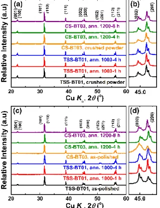
surfaces (c, d) measured at RT for TSS-BT01 and CS-BT03 ceramics. Measurement range is (a, c) 20˚< 2<60˚, (b, d) 44˚< 2 <46˚ for (002) and (200) peaks.. ... 52
Figure 2.2.2 Microstructures of two-step sintered (TSS) BT01 and conventionally sintered
(CS) BT03 ceramics. a) as-sintered BT01, b) 1000 oC- 1 h annealed BT01, c) 1000 oC- 4 h
annealed BT01, d) as-sintered BT03, e) 1200 oC- 4 h annealed BT03, and e) 1200 oC- 8 h
annealed BT03. (Note: The magnification used is 2000 for a-c, while it is 1000 for d-f) SEM images.. ... 54
Figure 2.2.3 Dielectric constant as a function of grain size in thermally annealed BaTiO3
ceramics. ... 55
Figure 2.2.4 Ferroelectric properties in thermally annealed BT ceramics. (a) Bipolar P- E
X
coercive field (Ec) with grain size. ... ... 56 Figure 2.2.5 Frequency dependence of impedance and phase in poled BT01 (a-c) and BT03
(d-f) ceramics. a) without annealing, b) annealed at 1000 oC-1 h, c) annealed at 1000 oC-4 h,
d) without annealing, e) annealed at 1200 oC-4 h, and f) annealed at 1200 oC-8 h. .. ... 57 Figure 2.2.6 Grain-size dependence of piezoelectric constant in poled BaTiO3 ceramics prepared by various methods. ... 59
Chapter 3
Figure 3.1 The absolute and relative density of x(Bi0.5K0.5)TiO3-0.23BaTiO3
-0.02Bi(Mg0.5Ti0.5)O3-(0.75-x)BiFeO3 ceramics as a function (Bi0.5K0.5)TiO3
concentration. . ... 68
Figure 3.2 The Cu K X-ray diffraction patterns of x(Bi0.5K0.5)TiO3-0.23BaTiO3
-0.02Bi(Mg0.5Ti0.5)O3-(0.75-x)BiFeO3 ceramics as a function of (Bi0.5K0.5)TiO3 concentration.
... 69
Figure 3.3 X-ray diffraction patterns of x(Bi0.5K0.5)TiO3-0.23BaTiO3-0.02Bi(Mg0.5Ti0.5)O3
-(0.75-x)BiFeO3 ceramics as a function of (Bi0.5K0.5)TiO3 concentration with selected 2 in
range of (a) 31o ≤ 2 ≤ 33o for (110)
C, (b) 38o ≤ 2 ≤ 40o for (111)C, and (c) 45o ≤ 2 ≤ 46o
for (200)C. ... 69 Figure 3.4 SEM images of as-sintered x(Bi0.5K0.5)TiO3-0.23BaTiO3-0.02Bi(Mg0.5Ti0.5)O3
-(0.75-x)BiFeO3 ceramics as a function of (Bi0.5K0.5)TiO3 concentration. ... 70 Figure 3.5 Bipolar P-E hysteresis loops measured at room temperature with AC bias of 0.1
Hz for x(Bi0.5K0.5)TiO3-0.23BaTiO3-0.02Bi(Mg0.5Ti0.5)O3-(0.75-x)BiFeO3 ceramics as a
function of (Bi0.5K0.5)TiO3 concentration. ... 70 Figure 3.6 Bipolar S-E curves measured at room temperature with AC bias of 0.1 Hz for
x(Bi0.5K0.5)TiO3-0.23BaTiO3-0.02Bi(Mg0.5Ti0.5)O3-(0.75-x)BiFeO3 ceramics as a function of
(Bi0.5K0.5)TiO3 concentration. ... 71 Figure 3.7 Frequency dependence of dielectric constant and loss factor in x(Bi0.5K0.5)TiO3
-0.23BaTiO3-0.02Bi(Mg0.5Ti0.5)O3-(0.75-x)BiFeO3 ceramics as a function of (Bi0.5K0.5)TiO3
concentration. ... 72
Figure 3.8 Temperature dependence of dielectric constant (measured at 1 kHz) in
x(Bi0.5K0.5)TiO3-0.23BaTiO3-0.02Bi(Mg0.5Ti0.5)O3-(0.75-x)BiFeO3 ceramics as a function of
(Bi0.5K0.5)TiO3 concentration. ... 73 Figure 3.9 Temperature dependence of dielectric loss factor (measured at 1 kHz) in
XI
x(Bi0.5K0.5)TiO3-0.23BaTiO3-0.02Bi(Mg0.5Ti0.5)O3-(0.75-x)BiFeO3 ceramics as a function of
(Bi0.5K0.5)TiO3 concentration. ... 73 Figure 3.10 Piezoelectric strain constant, Curie temperature, and coercive field in
x(Bi0.5K0.5)TiO3-0.23BaTiO3-0.02Bi(Mg0.5Ti0.5)O3-(0.75-x)BiFeO3 ceramics as a function of
(Bi0.5K0.5)TiO3 concentration. ... 74
Chapter 4
Figure 4.1 Engineered domain structures and monodomain states in 3m rhombohedral (R),
mm2 orthorhombic (O), and 4mm tetragonal (T) ferroelectric phases after poling at sufficiently high fields along <001>C, <011>C, and <111>C directions. ... 83 Figure 4.2.1 Scanning electron microscopy image of the H1.08Ti1.73O4.nH2O (HTO) template
particles. ... 86
Figure 4.2.2 Schematic diagram of RTGG method and mechanism of grain-orientation. .. 87 Figure 4.3.1 Surface X-ray diffraction (XRD) patterns of BaTiO3 ceramics prepared using HTO template and BaCO3 matrix particles sintered at various temperatures. The powder
XRD patterns is included for the comparison. . ... 90
Figure 4.3.2 Relative density and grain-orientation factor as a function of sintering
temperature.. ... 91
Figure 4.3.3 Microstructures of surface of the as-sintered BaTiO3 ceramics as a function of sintering temperature. . ... 92
Figure 4.3.4 Microstructures of fractured surface of the as-sintered BaTiO3 ceramics as a function of sintering temperature. ... 93
Figure 4.4.1 SEM images of (Bi0.5K0.5)TiO3 green compacts in the plane perpendicular (a)
and parallel (b) to the sheet-stacking direction. ... 100
Figure 4.4.2 One- and three-step sintered BKT ceramics’ a) XRD patterns, and
microstructure [(b); one-step and (c) three-step sintered] in the plane parallel to the sheet-stacking direction. . ... 101
Figure 4.4.3 Effect of weighted sintering (WS) and weighted and embedded sintering (WES)
on XRD patterns (a) and microstructures of b) one-step WS, c) one-step WES, d) three-step WS, and e) three-step WES BKT ceramics. ... 104
Figure 4.4.4 Microstructure of the sample debinded (600 oC-5 h) without weight-pressing (a,
XII
sheet-stacking direction. ... 105
Figure 4.4.5 Comparison of grain-orientation factor (F100) in three-step conventional sintered (CS)-, WS-, and WES-BKT ceramics as a function debinding and weighted debinding treatment prior to sintering. ... 106
Figure 4.4.6 a) XRD patterns, and microstructure of the weighted-debinded (WD) BKT
ceramics sintered by three-step WES without (b, c) and with (d, e) CIP treatment. (Note: (b) and (d) are the SEM images of the plane perpendicular to the sheet-stacking direction, while (c) and (e) are for the plane parallel to the sheet-stacking direction.). ... 107
Figure 4.5.1 Schematic diagram of formation mechanism of the plate-like BaTiO3
nanoparticles.1 ... 113 Figure 4.5.2 Schematic diagram of formation mechanism of the plate-like (Bi0.5Na0.5)TiO3
mesocrystals.2 ... 114
Chapter 5
Figure 5.1.1 XRD patterns of the polished surfaces of the
0.11BKT-0.23BT-0.02BMT-0.64BF ceramics sintered at 1000 oC for 2 h. ... 120 Figure 5.1.2 SEM images of the mirror polished surfaces of the
0.11BKT-0.23BT-0.02BMT-0.64BF ceramics sintered at 1000 oC for 2 h prepared using; a) 1st approach, b) 2nd approach,
and c) 3rd approach. ... 121 Figure 5.1.3 XRD patterns of the surfaces of the 0.11BKT-0.23BT-0.02BMT-0.64BF
ceramics, prepared using the first approach, as a function of sintering temperature. . ... 122
Figure 5.1.4 XRD patterns of the surfaces of the 0.11BKT-0.23BT-0.02BMT-0.64BF
ceramics, prepared using the first approach, as a function of sintering temperature with selected with selected 2 in range of (a) 38o ≤ 2 ≤ 40o for (111)
C, (b) 45o ≤ 2 ≤ 46o for
(200)C. . ... 123 Figure 5.1.5 SEM images of the surfaces (perpendicular to sheet-stacking direction) of the
0.11BKT-0.23BT-0.02BMT-0.64BF ceramics prepared from the 1st experimental approach
as a function of sintering temperatures. ... 124
Figure 5.1.6 SEM images of the fractured surfaces (parallel to sheet-stacking direction) of
the 0.11BKT-0.23BT-0.02BMT-0.64BF ceramics prepared from the 1st experimental
approach as a function of sintering temperatures. ... 125
Figure 5.2.1 Surface XRD patterns of 0.11BKT-0.23BT-0.02BMT-0.64BF ceramics,
XIII
Figure 5.2.2 Surface XRD patterns of 0.11BKT-0.23BT-0.02BMT-0.64BF ceramics,
prepared using the HTO-Bi2O3-KHCO3-MgO-Fe2O3-BaCO3 reaction system, under different
debinding and sintering conditions. (Sintering was done at 1025 oC for 2 h.). ... 132 Figure 5.2.3 SEM images of the 0.11BKT-0.23BT-0.02BMT-0.64BF ceramics, prepared using the HTO-Bi2O3-KHCO3-MgO-Fe2O3-BaCO3 reaction system, with different debinding
and sintering conditions. (Sintering was done at 1025 oC for 2 h.). ……….133 Figure 5.2.4 Relative density (a) and grain-orientation factor (F100) as a function of sintering temperature in the debinded and weighted-debinded 0.11BKT-0.23BT-0.02BMT-0.64BF ceramics prepared using the HTO-Bi2O3-KHCO3-MgO-Fe2O3-BaCO3 reaction system.
(Sintering was done with weight pressing; WS). ... 134
Figure 5.2.5 Surface XRD patterns of 0.11BKT-0.23BT-0.02BMT-0.64BF ceramics,
prepared using the HTO-Bi2O3-KHCO3-MgO-Fe2O3-BaCO3 reaction system, as a function
of sintering temperatures. ... 136
Figure 5.2.6 Surface XRD patterns of 0.11BKT-0.23BT-0.02BMT-0.64BF ceramics,
prepared using the HTO-Bi2O3-KHCO3-MgO-BiFeO3-BaCO3 reaction system, as a function
of sintering temperatures. ... 137
Figure 5.3.1 Schematic diagram of (a) <110>- and (b) <100>-orientation mechanism in
0.11BKT-0.23BT-0.02BMT-0.64BF ceramics. ... 140
Chapter 6
Figure 6.1 Surface XRD patterns of the <110>- and <100>-oriented
0.11BKT-0.23BT-0.02BMT-0.64BF ceramics, prepared using different reaction systems... 146
Figure 6.2 Frequency-dependent dielectric constant and dielectric loss factor in
0.11BKT-0.23BT-0.02BMT-0.64BF ceramics without and with <110>- and <100>-orientation. ... 147
Figure 6.3 Temperature-dependent dielectric constant (a) and dielectric loss factor (b) in
0.11BKT-0.23BT-0.02BMT-0.64BF ceramics without and with <110>- and <100>-orientation. ... 148
Figure 6.4 Bipolar polarization-electric field (P-E) loops in (a) non-orientated, (b)
<110>-orientated, and (c) <100>-orientated 0.11BKT-0.23BT-0.02BMT-0.64BF ceramics. ... 149
Figure 6.5 Bipolar strain-electric field (S-E) curves in (a) non-orientated, (b)
<110>-orientated, and (c) <100>-orientated 0.11BKT-0.23BT-0.02BMT-0.64BF ceramics. ... 150
Figure 6.6 Unipolar strain-electric field (S-E) curves in (a) non-orientated, (b)
XIV
Figure 6.7 Comparison of piezoelectric strain constant (d33*) in lead-based and various lead-
free piezoelectric ceramics. [References: 25-38]. ... 152
Figure 6.8 Unipolar S-E curves in randomly- and <100>-oriented
0.11BKT-0.23BT-0.02BMT-0.64BF piezoelectric ceramics.. ... 154
Figure 6.9 Unipolar S-E curves in <100>-oriented 0.11BKT-0.23BT-0.02BMT-0.64BF
piezoelectric ceramics water-quenched after thermal annealing at 800 oC for 1 or 20 h... 155
LIST OF TABLES
Chapter 2
Table 2.1.1 Dielectric properties of unpoled BT ceramics which were annealed at different
temperatures after polishing and/or cutting. The values of relative density, grain sizes, and Curie point TC data are also included. WA refers to the samples without annealing. (Note: TC
values are determined from the peaks in the dielectric constant vs. temperature curves measured during heating.) ... 26
Table 2.1.2 Piezoelectric properties of poled BT ceramics which were annealed at different
temperatures after polishing and/or cutting. The values of phase angles are also included. WA refers to the samples without annealing. ... 43
Table 2.2.1 Various properties parameters in BaTiO3 ceramics (Note: TSS = two-step sintering, CS = conventional sintering, WA = without annealing, A10 = annealing at 1000 oC,
and A12 = annealing at 1200 oC). ... 58
Chapter 5
Table 5.1.1 Combination of matrix-materials and HTO template particles used in the
different experimental approaches for preparing <110>-oriented ceramics. ... 119
Table 5.2.1 Combination of matrix-materials and HTO template particles used in the
1
Chapter 1 Introduction and Background
In this section, we review the basic concept of piezoelectricity and ferroelectricity. In addition, we briefly describe the strategy of piezoelectricity enhancement in lead-free ceramics and concept of domain engineering by crystallographic-axis orientation and domain-size control.
1.1 Piezoelectricity and related parameters
Piezoelectricity literally means a pressure electricity. The piezoelectric materials possess two interesting physical properties. One is the generation of electrical polarization proportional to an applied mechanical stress; direct piezoelectric effect, and other is the mechanical deformation of the crystal proportional to an applied electric field; converse piezoelectric effect. Jacques Curie and Pierre Curie first discovered the direct piezoelectricity in quartz crystals in 1880.1 After 1 year
of the discovery of the direct piezoelectric effect, again Curie brothers verified the converse effect after the prediction by Lippmann.2 The piezoelectricity found in the quartz crystals and rochelle
salt were used in the ultrasonic transducers before the end of World War-I. Nowadays, piezoelectric materials are widely used in various areas of science and technology. The sensors utilizing the piezoelectric effect convert mechanical signals into electrical signals and are used as accelerometers, and for measurements of pressure and vibration. On the other hand, the piezoelectric actuators transform electrical signals into mechanical signals and are used in displacement actuators and force generators.
1.1.1 Dielectric permittivity
The dependency of electric displacement in the dielectric material to the applied electric field is given by the following relation:
2
Di = εij. Ej (1) where εij is the dielectric permittivity of the material and Ej is the applied electric field. The relative
dielectric permittivity εr(ij) which is commonly referred to the dielectric constant of the material is
the ratio of the dielectric permittivity and permittivity of free space. The dielectric permittivity is mainly associated with the electronic and ionic polarizabilities in simple inorganic solids, while
Figure 1.1 Idealized strain-electric field hysteresis loops showing lattice expansion
3
the domain walls and polarization rotation have significant contribution to dielectric properties in ferroelectric materials.3,4 The dielectric permittivity has two components; one is real (ε
rʹ) and the
other is the imaginary components (εrʹʹ), which are connected by the following equation.
εrʹʹ = εrʹ. tanδ (2) where tanδis the dielectric loss.
1.1.2 Piezoelectric coefficients
Piezoelectric effect is the linear coupling between mechanical stress and electric polarization and/or between mechanical strain and applied electric field. 3,4 The direct piezoelectric effect is
caused by polarization change when mechanical energy is applied. Changes in polarization are caused by rearrangement of dipoles due to changes in the dipoles-inducing-surrounding environment, or changes in the direction of dipole moment due to changes in the direction in which molecules are arranged due to external stress. Therefore, the direct piezoelectric effect is revealed when the change in direction and size of polarization is occurred.
The converse piezoelectric effect is revealed by mechanical deformation generated when an external electric field is applied, contrary to the direct piezoelectric effect. The converse piezoelectric effect is exhibited with bipolar strain – electric field curve as shown in Figure 1.1. When electric field and polarization are parallel, the lattice is expanded along the direction of electric field as shown in Figure 1.1(a) and 1.1(c), which is positive stain. On the other hand, the lattice is shrunk when polarization and electric field are antiparallel as shown in Figure 1.1(b) and 1.1(d), which is negative strain. The direct piezoelectric effect and the converse piezoelectric effect are expressed by the following equations.
4
D = dT + εE (3) S = sT + dTE (4)
where D is electric displacement. E is electric field. S and T are strain and stress, respectively. d and s are piezoelectric constant and elastic compliance constant, respectively. ε is dielectric permittivity.5 According to the equation, at constant electric field (E) and mechanical stress (T),
the piezoelectric charge (or strain) coefficient d can be expressed as a proportional relationship between displacement and stress or deformation and electric field as follows.
d = (∂D
∂T)E = ( ∂S
∂E)T (5)
Based on the above formula, the unit of the piezoelectric charge constant (d33) is pC/N and the
piezoelectric strain constant (d33*) is pm/V, respectively. 1.2 Ferroelectricity and related parameters
Ferroelectricity refers to presence of spontaneous polarization in the materials that can be reoriented between two or more distinct crystallographic directions by the application of an external electric field.6-8 The polarization reorientation can also occur by the application of
mechanical stress (ferroelastic switching) which is different from ferroelectric switching where polarization reorientation is caused by the applied external electric field.
1.2.1 Ferroelectric domains and domain walls
When a ferroelectric crystal is cooled from the centrosymmetric paraelectric to non-centrosymmetric ferroelectric phase with lower symmetry through phase-transition temperature commonly called as the Curie temperature, a spontaneous polarization is developed by the shift of
5
O and B-site cations relative to A-site cations. Directions along which the spontaneous polarization will develop depends on the crystallographic-orientation achieved after cooling from the Curie temperature. Regions with uniform polarization are called ferroelectric domains and their length ranges from few nanometers to several micrometers. The interface between two domains is called the domain wall with the scale of a few lattice cells. The ferroelectric domains are formed to minimize the electrostatic energy of the depolarizing fields and the elastic energy associated with the mechanical constraints to which the ferroelectric material is subjected as it is cooled through the paraelectric to ferroelectric phase transition.9-11 Development of spontaneous polarization at
the transition temperature leads to the formation of surface charges that produces an electric field, called the depolarizing field Ed, which is oriented oppositely to Ps (Fig. 1.2). The depolarizing field
will form whenever there is a nonhomogeneous distribution of the spontaneous polarization, for example, due to the fall-off of the polarization near the surface of the ferroelectric (polarization is zero outside the ferroelectric and nonzero inside) or due to a change in the direction of the
Figure 1.2 90o and 180o ferroelectric domain walls formation in a tetragonal perovskite
ferroelectric. The deformation of the crystal in the domain-wall region due to the formation of 90◦ walls is exaggerated for the sake of picture clarity.
6
polarization at grain boundaries. The depolarizing field may be very strong (of the order of MV/m) rendering the single-domain state of the ferroelectric energetically unfavorable.9,10 The
electrostatic energy associated with the depolarizing field may be minimized either by the ferroelectric crystals splitting into domains with oppositely oriented polarization or by compensating the depolarizing charge by electrical conduction through the crystal or by charges from the surrounding material. Usually, the depolarizing field cannot be fully compensated as a result of which as-grown ferroelectric crystals often exhibit reduced or even zero piezoelectric effects. Splitting of a ferroelectric crystal into domains may also occur due to the influence of mechanical stresses, as shown in Fig. 1.2.11,12 For example, when a part of PbTiO
3 crystal is
mechanically compressed along the <100> cubic direction as it is cooled through the phase-transition temperature. To minimize the elastic energy, the long cT-axis of the tetragonal cell will
develop perpendicularly to the stress. In the unstressed part of the crystal, the polarization may remain parallel to the direction of the stress (short aT-axis perpendicular to the stress). The domain
walls in PbTiO3 may therefore separate regions in which polarization orientation is antiparallel
(180o walls) or perpendicular (90o walls) to each other. Both 90o and 180◦ walls may reduce the
effects of depolarizing electric fields but only the formation of 90o walls may minimize the elastic
energy. A combination of electrical and elastic boundary conditions to which a crystal is subjected as it is cooled through the ferroelectric phase-transition temperature usually leads to a complex domain structure with many 90o and 180o walls. Since domain walls themselves carry energy, the
resulting domain-wall configuration will be such that the sum of the domain-wall energy, crystal surface energy, and elastic and electric fields energy is minimal.9,11 The domain walls that differ in
orientation from the spontaneous polarization vector are called ferroelectric domain walls and those that differ in orientation from the spontaneous strain tensor are called ferroelastic domain
7
walls. In PbTiO3, the 180o walls are purely ferroelectric because they differ only in orientation of
the polarization vector. The 90o walls are both ferroelectric and ferroelastic, as they differ in
orientation of both the polarization vector and the spontaneous strain tensor.12 The types of domain
walls that can occur in a ferroelectric crystal depend on the symmetry of both non-ferroelectric and ferroelectric phases of the crystal.13
For the tetragonal (T) case, domains can have their polarization along one of the six <001> directions, while for a rhombohedral (R) phase, the spontaneous polarization lies along one of the eight <111> directions with 180o and 71o/109o domain walls. On the other hand, in the
orthorhombic (O) phase, 180o, 60o, 90o, and 120o domain walls may exist, with spontaneous
polarization lies along one of twelve <011> directions. The switching of 180o domain walls does
not involve elastic deformation (so called ferroelectric domain walls), while the switching of non-180o walls involves elastic deformation, referred to as ferroelastic domain walls. Thus, both 180o
and non-180o domain walls may reduce the effects of depolarizing electric fields, but only the
formation of non-180o domain walls can minimize the elastic energy. It is believed that the
dielectric loss is related to the 180o and non-180o domain wall motion under an applied electric
field, while mechanical loss is only associated with non-180o domain wall motion under an applied
stress.
1.2.2 Ferroelectric hysteresis loops
A polarization-electric field hysteresis loops is the characteristics features of a ferroelectric material. Ferroelectrics show strong non-linear dielectric behavior, thus, the polarization as a function of applied ac electric field (E) is generally hysteretic due to the domain wall motion as shown in Figure 1.3. Initially, ferroelectric domains are randomly distributed. With the application
8
of electric field, the ferroelectric domain aligns along the direction of the applied electric field. And the polarization is saturated despite the increasing electric field which is called saturated polarization (Ps). Even after the removal of the applied external electric field, a certain polarization
value is retained caused by the remaining directional domain, which is called remanent polarization (Pr). The critical electric field that is required to switch the ferroelectric domain in the
opposite direction is called the coercive electric field (Ec). An ideal hysteresis loop is symmetrical
with same value of the positive and negative coercive fields and positive and negative remanent polarizations are also equal. The coercive field, spontaneous and remanent polarization, and shape of the loop may be affected by many factors including the thickness of the sample, presence of
Figure 1.3 A typical polarization-electric field (P-E) hysteresis loop with
9
charged defects, mechanical stresses, preparation conditions, and thermal treatment.
The as-prepared polycrystalline ferroelectric ceramics do not exhibit piezoelectric properties due to the presence of randomly oriented domains or cancellation of polarization to zero net macroscopic polarization. However, polycrystalline ferroelectric materials (ceramics) may be brought into a polar state by applying a strong electric field (10-100 kV/cm), usually at elevated temperatures. This process, called poling, can reorient domains within individual grains along those directions that are permissible by the crystal symmetry and that lie as close as possible to the direction of the field. A poled polycrystalline ferroelectric exhibits piezoelectric properties despite the presence of many domains as shown in Fig. 1.4.
1.3 Current status of lead-free piezoelectric ceramics
The lead-based piezoelectric ceramics are widely used in the various electromechanical devices, because of their high piezoelectric property near the morphotropic phase boundary (MPB) composition.14-16 The highest piezoelectric coefficient and dielectric constant, and planar
electromechanical coupling factor (kp) are observed in PZT with MPB as shown in Fig. 1.5.17,18 Figure 1.4 A polycrystalline ferroelectric with random orientation of grains before and after
poling. Many domain walls are present in the poled material, however, the net remanent polarization is nonzero.
10
However, the toxicity of lead and oxide has demanded the development of alternative lead-free piezoelectric materials that are environmentally benign from the viewpoint of sustainable development.19-21 Various lead-free piezoelectric ceramics has been studied to replace lead-based
piezoelectric ceramics. BaTiO3 (BT) is the prototypical ferroelectric material, well known for its
large piezoelectric response,22,23 however, the Curie temperature (T
C) of around 130 oC24,25 has
limited its application in diverse areas. The large piezoelectric properties have been reported for various BT-based lead-free piezoelectric ceramics such as (Bi,Na)TiO3-BaTiO3 (BNT-BT)26,27 and
Ba(Ti,Zr)O3-(Ba,Ca)TiO3 (BTZ-BCT).28 The BNT-BT based system has a giant strain,29-32
however, the depolarization temperature has limited its real application.31 On the other hand, the
BTZ-BCT system has a large charge constant (d33) which is approximately 620 pC/N. However,
this system is difficult to use in the real application, because of its low TC (93 oC).28
The (K, Na) NbO3 (KNN) is also attracting attention as a lead-free piezoelectric material, which Figure 1.5 The piezoelectric coefficient and dielectric constant, and planar electromechanical
11
has been studied extensively. It is reported that characteristics of KNN-based lead-free piezoelectric materials are similar shown to those of commercial PZT.33 In addition, excellent
piezoelectric properties are exhibited around room temperature where the crystal structure is changed from orthorhombic to tetragonal structure. However, the hygroscopic nature of Na has been the impediment for this system.34,35
The BiFeO3 (BFO) materials have long been studied and are well-known for their high
polarization36 and high TC (~ 1100 K).37,38 However, the reported d33 (~ 4.2 pC/N)39 of BFO is
extremely low, which could be enhanced by making its solid solution with BT, (Bi0.5K0.5)TiO3
(BKT), and BNT.40-44 The piezoelectric coefficient as a function of Curie temperature in various lead-free ceramics along with that of the lead-based one is shown in Fig. 1.6. Several reports have
Figure 1.6 Piezoelectric constant as a function of Curie temperature in lead-free
12
pointed out the BT, BNT-based, BKT-based, and KNN-based systems as the promising candidate lead-free systems.
In 2004, Saito et al. reported <001> oriented KNN-based composition with piezoelectric properties comparable to that of Pb-based one with a d33 of 416 pCN-1 and TC of 253 oC, which is
attributed to the MPB composition and grain orientation. However, piezoelectric properties superior to that of the lead-based systems seem to be difficult to achieve only by compositional engineering with MPB or polymorphic phase transition. Thus, to exceed the properties of lead-based ceramics, domain engineering could be one of the approaches.
1.4 Domain engineering by crystallographic orientation
The domain configurations (number of domains and possible orientation) of a ferroelectric material which are affected by the crystallographic symmetry have been reported to affect the dielectric and piezoelectric properties. The process of achieving desirable domain configuration is called domain engineering. A domain engineered ferroelectric crystal has been defined as the crystal that has been poled along one of the possible polar axes of the crystal other than the zero-field polar axis, creating a set of domains (polydomain state) in which the polarizations are oriented so that their angles to the poling direction are minimized.45 Piezoelectric constant d33>2500 pC/N
and strain levels up to >0.6% with minimal hysteresis were achieved for the <001>-oriented rhombohedral relaxor-PT single crystal, while the piezoelectric constant was ~80 pC/N along the polar <111> direction. The lower piezoelectric properties of the <111>-oriented crystals was strongly related to domain instability. In contrast, the ultrahigh piezoelectric properties of the <001>-orientated crystals caused by the stable domain configurations. <111> is the polar direction in rhombohedral crystal with eight degenerate domain variants. After poling along <001>
13
direction, four out of the eight domain variants will be energetically favored by the poling field. Thus, the <001> poled crystals have the domain configuration where each domain has one of four possible polar directions -<111>, <-111>, <1-11> and <-1-11>.46 Thus, four domain variants existed after poling treatment, with polar vectors equally inclined to the poling direction (~54.7o), thereby exhibiting a macroscopic 4mm symmetry. The resultant engineered domain configuration will be stable upon the increment of the electric field along the poling direction due to the lack of driving force for domain wall motion. Only the polar vector in each variant will rotate towards the direction of the applied field by polarization rotation or inclination.47 An engineered domain configuration which is usually a multidomain state can be achieved in crystals with different crystal symmetries by different crystallographic orientation (details will be discussed in chapter 4.1). The ultrahigh piezoelectric properties in engineered domain configurations of relaxor-PT single crystals were due to the easy spontaneous polarization tilting by the electric field applied along non-polar directions. A domain wall engineering using patterning electrodes or special poling process, could also increase the piezoelectric activity with increasing domain wall densities (decreasing domain sizes) in BaTiO3 or PMNPT crystals,48-51 due to the extrinsic contribution from
the domain wall density.
1.5 Domain engineering by domain size control
The concept of domain engineering was applied to lead-free BaTiO3 polycrystalline ceramics.
The <110>-textured BaTiO3 ceramics, prepared using the templated grain growth method,
exhibited piezoelectric constant of 788 pC/N.52 The <110>-textured ceramics, possessing an
identical grain size (75 µm) and comparable degree of texturing [<110>-orientation factor of 82.2 and 84.6%], exhibited the piezoelectric coefficient of 507 and 788 pC/N for the domain size of 1.2
14
and 0.8 µm, respectively. These results strongly suggested that domains with smaller size are good for piezoelectric enhancement. Thus, for the further enhancement of piezoelectric properties, fabrication of ceramics with smaller grain size was suggested as domain size in bulk ferroelectric ceramics has been reported to be an exponential function of grain size.53
1.6 Strategy for high performance lead-free piezoelectric ceramic
Besides the crystallographic orientations, a chemical composition of the ceramics may also determine the nature of domains. The existence of polar nanoregions in relaxor Pb-based materials such as Pb(Mg1/3Nb2/3)O3 (PMN) and Pb(Zn1/3Nb2/3)O3 (PZN) have also been suggested to play
important roles in influencing the piezoelectric performance of relaxor-PbTiO3 piezoelectric
systems.54,55 Following the findings of ultrahigh piezoelectric properties in relaxor-ferroelectric
system of Pb-based materials, researches on various solid solutions of relaxor and typical ferroelectrics have been spurred recently for the lead-free ceramics as well.56-58 A solid solution of
BaTiO3-(Bi0.5K0.5)TiO3 and BaTiO3- Bi(Mg0.5Ti0.5)O3 has been reported to relaxor-like
characteristics, while BiFeO3 is a well-known ferroelectric materials. Thus, the solid solution of
relaxor materials consisting polar nanoregions and ferroelectrics materials consisting large ferroelectric domains is expected to have higher domain wall density with a formation of nano-macro domain. The solid solution of BaTiO3, Bi(Mg0.5Ti0.5)O3, and BiFeO3 was prepared where
the domain structure of the 0.3BaTiO3-0.1Bi(Mg0.5Ti0.5)O3-0.6BiFeO3 (0.3BT-0.1BMT-0.6BF)
ceramics was mainly composed of nanodomains with a small amount of large, ferroelectric domains (macrodomains).58 Therefore, in this thesis the preparation and characterization of solid
solutions of lead-free (Bi0.5K0.5)TiO3-BaTiO3-Bi(Mg0.5Ti0.5)O3-BiFeO3 (BKT-BT-BMT-BF)
15
conditions, the adopted target in this thesis is to prepare environment-friendly lead-free piezoelectric ceramics with Curie temperature higher than 400 oC and piezoelectric coefficient
higher than 600 pC/N (pm/V). The development of lead-free piezoelectric ceramics that are capable of replacing lead-based piezoelectric systems with a wide range of working temperatures are focused in this study.
In order to achieve enhanced piezoelectric properties, the grain orientation technique that is suitable for creating engineered domain configurations for the optimum chemical composition of (Bi0.5K0.5)TiO3-BaTiO3-Bi(Mg0.5Ti0.5)O3-BiFeO3 (BKT-BT-BMT-BF) piezoelectric ceramics will
be furthermore applied.
1.7 Outline of the thesis
In this chapter, the basic concept of piezoelectricity, ferroelectricity, lead-free piezoelectric ceramics, domain engineering by crystallographic orientation and domain-size control, strategy for piezoelectric properties enhancement was introduced.
In the first part of chapter 2, the impact of mechanical processing (polishing and cutting) on the dielectric, ferroelectric, and piezoelectric properties of prototypical ferroelectric BaTiO3 are
presented. And in the second part, the piezoelectric and ferroelectric properties of BaTiO3 ceramics
after subjecting to thermal treatment are discussed as a function of grain size.
In chapter 3, the optimum chemical composition of lead-free Bi-based x(Bi0.5K0.5)TiO3
-0.23BaTiO3-0.02Bi(Mg0.5Ti0.5)O3-(0.75-x)BiFeO3 [xBKT-0.23BT-0.02BMT-(0.75-x)BF; with x =
0.05, 0.07, 0.09, 0.11] ceramics for higher piezoelectric performance along with higher TC is
16
dielectric, ferroelectric, and piezoelectric properties, however, they were found to be insufficient for practical application.
In chapter 4, the concept of domain engineering and the preparation method of grain-oriented ceramics are discussed. The grain orientation direction in BaTiO3 and Bi0.5K0.5)TiO3 ceramics
prepared using the HTO template particles were investigated to assess the possibility of texturing using oriented BaTiO3 and (Bi0.5K0.5)TiO3 end members as crystal seeds.
In chapter 5, the optimum preparation conditions for the synthesis of <110>- and <100>-textured Bi-based 0.11BKT-0.23BT-0.02BMT-0.64BF ceramics are discussed, while in chapter 6, the dielectric, ferroelectric, and piezoelectric properties of the randomly-oriented, and <110>- and <100>-oriented ceramics are discussed. The significance of properties of textured ceramics is also presented in chapter 6. Finally, the discussion of results are concluded in the Chapter 7.
References
1J. Curie and P. Curie, Bull. Soc. Fr. Mineral. 3, 90 (1880).
2G. Lippman, Ann. Chim. Phys. 24, 145 (1881).
3N. Setter, “ABC of piezoelectricity and piezoelectric materials,” in Piezoelectric Materials in
Devices, edited by N. Setter (Lausanne, Switzerland, 2002), pp. 1–27.
4R. E. Newnham, Properties of Materials-Anisotropy, Symmetry, Structure (Oxford University
Press, NY, 2005).
5K. Lefki and G. J. M. Dormans, J. Appl. Phys. 76, 1764 (1994).
6K. Uchino, Ferroelectric Devices (CRC, NY, 2009).
17 (Clarendon, Oxford, 1977).
8L. E. Cross, “Ferroelectric ceramics: Tailoring properties for specific applications,” in
Ferroelectric Ceramics: Tutorial Reviews, Theory, Processing and Applications, edited by N. Setter and E. L. Colla (Birkhauser, Basel, 1993), pp. 1–87.
9M. E. Lines and A. M. Glass, Principles and Applications of Ferroelectrics and Related Materials,
Clarendon, Oxford (1979).
10J. C. Burfoot and G. W. Taylor, Polar Dielectrics and Their Applications, Macmillan, London
(1979).
11G. Arlt, ‘Twinning in ferroelectric and ferroelastic ceramics: stress relief,’ J. Mat. Sci. 25,
2655--2666 (1990).
12R. E. Newnham, Structure-Property Relations, Springer-Verlag, Berlin (1975).
13J. Fousek and V. Janovec, ‘The orientation of domain walls in twinned ferroelectric crystals,’ J.
Appl. Phys. 40, 135--142 (1969).
14B. Jaffe, W. R. Cook, and H. Jaffe, Piezoelectric Ceramics (Academic, London, 1997).
15C. K. Jeong, J. Lee, S. Han, J. Ryu, G.-T. Hwang, D. Y. Park, J. H. Park, S. S. Lee, M. Byun, S.
H. Ko, and K. J. Lee, Adv. Mater. 27, 2866 (2015).
16Piezoelectric actuator and ultrasonic motors, edited by K. Uchino (Kluwer Academic Publishers,
Boston, 1997).
17S. Zhang, R. Xia, and T. R. Shrout, J. Electroceram. 19, 251 (2007).
18B. Jaffe, R. S. Roth, and S. Marzullo, J. Appl. Phys. 25, 809 (1954).
18
20J. Rödel, W. Jo, K. T. P. Seifert, E-M. Anton, and T. Granzow, J. Am. Ceram. Soc. 92 [6], 1153
(2009).
21J. Rödel, K. G. Webber, R. Dittmer, W. Jo, M. Kimura, and D. Damjanovic, J. Eur. Ceram. Soc.
35, 1659 (2015).
22H. Takahashi, Y. Numamoto, J. Tani, and S. Tsurekawa, Jpn. J. Appl. Phys. 45, 7405 (2006).
23S. Shao, J. Zhang, Z. Zhang, P. Zheng, M. Zhao, J. Li, and C. Wang, J. Phys. D: Appl. Phys. 42,
189801 (2009).
24K. Sakayori, Y. Matsui, H. Abe, E. Nakamura, M. Kenmoku, T. Hara, D. Ishikawa, A. Kokubu,
K. Hirota, and T. Ikeda, Jpn. J. Appl. Phys. 34, 5443 (1995).
25K. Kinoshita and A. Yamaji, J. Appl. Phys. 47, 371 (1976).
26Y. S. Sung, J. M. Kim, J. H. Cho, T. K. Song, M. H. Kim, and T. G. Park, Appl. Phys. Lett. 96,
202901 (2010).
27W. Zeng, X. Zhou, J. Chen, J. Liao, C. Zhou, Z. Cen, T. Yang, H. Yang, Q. Zhou, G. Chen, and
C. Yuan, Appl. Phys. Lett. 104, 242910 (2014).
28W. Liu and X. Ren, Phys. Rev. Lett. 103, 257602 (2009).
29H.-S. Han, I.-K. Hong, Y.-M. Kong, J.-S. Lee, and W. Jo, J. Korean. Ceram. Soc. 53(2), 145
(2016).
30S.-T. Zhang, A. B. Kounga, E. Aulbach, H. Ehrenberg, and J. Rödel, Appl. Phys. Lett. 91, 112906
(2007).
19
32W. Jo, R. Dittmer, M. Acosta, J. Zang, C. Groh, E. Sapper, K. Wang, and J. Rödel, J. Electroceram.
29, 71 (2012).
33Y. Saito, H. Takao, T. Tani, T. Nonoyama, K. Takatori, T. Homma, T. Nagaya, M. Nakamura,
Nature 432, 84 (2004).
34G.H. Haertling, J. Am. Ceram. Soc. 50, 329 (1967).
35R. Zuo, J. Rödel, R. Chen, and L. Li, J. Am. Ceram. Soc. 89 [6], 2010 (2006).
36J. B. Neaton, C. Ederer, U. V. Waghmare, N. A. Spaldin, and K. M. Rabe, Phys. Rev. B 71,
014113 (2005).
37J. Wang, J. B. Neaton, H. Zheng, V. Nagarajan, S. B. Ogale, B. Liu, D. Viehland, V.
Vaithyanathan, D. G. Schlom, U. V. Waghmare, N. A. Spaldin, K. M. Rabe, M. Wutting, R. Rameshi, Science 299, 1719 (2003).
38I. M. Sosnowska, J. Microscopy. 236, 109 (2009).
39Z. Dai and Y. Akishige, J. Phys. D: Appl. Phys. 43, 445403 (2010).
40Y. J. Lee, J. S. Kim, S. H. Han, H.-W. Kang, H.-G. Lee, C. I. Cheon, J. Kor. Phys. Soc. 61, 947
(2012).
41Y. Wei, X. Wang, J. Zhu, X. Wang, and J. Jia, J. Am. Ceram. Soc. 96, 3163 (2013).
42Y. Wie, X. Wang, J. Jia, and X. Wang, Ceramics International 38, 3499 (2012).
43C. Zhou, X. Liu, and W. Li, Mater. Sci. Eng. B. 153, 31 (2008).
44Y. Li, N. Jiang, K. H. Lam, Y. Guo, Q. Zheng, Q. Li, W. Zhou, Y. Wan, and D. Lin, J. Am.
20
45A. J. Bell, J. Appl. Phys. 89(7), 3907-3914 (2001).
46S. E. Park and T. R. Shrout, J. Appl. Phys. 82, 1804 (1997).
47M. Davis, “Phase transitions, anisotropy and domain engineering: The piezoelectric properties
of realxor-ferroelectric single crystals,” Ph.D. dissertation (Swiss Federal Institute of Technology-EPFL, Lausanne, Switzerland, 2006).
48S. Wada, “Domain wall engineering in piezoelectric crystals with engineered domain
configuration,” in Handbook of Advanced Dielectric, Piezoelectric and Ferroelectric Materials – Synthesis, Characterization and Applications, edited by Z. G. Ye (Woodhead,
49S. Wada, K. Yato, H. Kakemoto, T. Tsurumi, and T. Kiguchi, J. Appl. Phys. 98, 014109 (2005).
50Y. Yamashita, N. Yamamoto, K. Itsumi, and Y. Hosono, Jpn. J. Appl. Phys. 50, 09NC05
(2011).Cambridge, England, 2008), pp. 266–303.
51D. Lin, S. J. Zhang, Z. Li, F. Li, Z. Xu, S. Wada, J. Luo, and T. R. Shrout, J. Appl. Phys. 100,
084110 (2011).
52S. Wada, K. Takeda, T. Muraishi, H. Kakemoto, T. Tsurumi, T Kimura, Jpn. J. Appl. Phys., 46,
7039 (2007).
53W. Cao, C. A. Randall, J. Phys. Chem. Solids, 57, 1499 (1996).
54X. Zhao, B. Fang, H. Cao, Y. Guo, H. Luo, Materials Science and Engineering B96, 254-262
(2002).
55F. Li, S. Zhang, T. Yang, Z. Xu, N. Zhang, G. Liu, J. Wang, J. Wang, Z. Cheng, Z. G. Ye, and J.
21
56I. Fujii, R. Mitsui, K. Nakashima, N. Kumada, H. Yabuta, M. Shimada, T. Watanabe, K. Miura,
and S. Wada, J. Ceram. Soc. Jpn. 121, 589-592 (2013).
57R. Mitsui, I. Fujii, K. Nakashima, N. Kumada, Y. Kuroiwa, and S. Wada, J. Ceram. Soc. Jpn. 121, 855-858 (2013).
58R. Mitsui, I. Fujii, K. Nakashima, N. Kumada, Y. Kuroiwa, and S. Wada, Ceramics International 39, S695-S699 (2013).
22
Chapter 2 Piezoelectricity enhancement in lead-free BaTiO3 piezoelectric ceramics by
domain engineering associated with grain-size control
2.1 Investigation of the effect of mechanical processing on electrical properties of lead-free BaTiO3 piezoelectric ceramics
2.1.1 Introduction
Piezoelectric materials with high piezoelectric coefficients are required for practical applications. The lead-based piezoelectric materials, for instance, Pb(ZrxTi1-x)O3 (PZT), Pb(Mg1/3Nb2/3)O3
-PbTiO3 (PMN-PT), Pb(Zn1/3Nb2/3)O3-PbTiO3 (PZN-PT), and their different modified forms have
dominated the market for years.1,2 The extensive investigations on environmentally friendly material systems are undergoing for the past twenty years owing to the various restrictions imposed on the use of hazardous Pb-containing materials regarding their toxicity.3,4 In this aspect, various mechanisms for the enhancement of dielectric, ferroelectric, and piezoelectric properties of lead-free materials have been exercised, which are compositional control with morphotropic phase boundary (MPB) composition5 and microstructure control on grain size,6-13 crystallographic texturing,14-18 and domain engineering.19 In addition, the physical properties of ferroelectrics can
be affected by the nature of raw materials, their stoichiometry, and processing techniques used.1 Importantly, it has been reported that strain and/or surface mechanical damage created during the mechanical processing could affect their ferroelectric and piezoelectric properties.20-22 Thus,
minimization of the imposed mechanical stress has been pointed out,23 although elimination of which in practicality is beyond the boundary of possibility. Therefore, the very basic and fundamental approach for piezoelectric enhancement is the optimization of processing techniques and it is crucial to understand the effect of strained or surface damaged layers on electromechanical
23
properties of ferroelectric materials. However, there have been very few systematic studies of the effect of strained or surface damaged layers on the electromechanical properties of ferroelectric materials. Heat treatment in air or other atmospheres has commonly been used to remove the surface defects and anomalous surface layers.24-26 Stress imposed on the ceramics’ surface is reported to be removed by thermal etching27 and chemical etching. Chemical etching of a strained surface layer of potassium niobate single domain crystal using HF and HNO3 exhibited an
enhancement of mechanical quality factor (Qm)from 4,002 to 7,613.28 On the other hand, the extent
of subsurface damage generated by the polishing of silicon carbide single crystal has been reported to be lowered by several folds after chemical mechanical polishing and hydrogen etching at high temperature.29 Furthermore, microscopic structure analysis near the mechanically polished surface of a PMN-PT single crystal suggested the presence of dislocations, which was found to affect the domain structure.20
In this study, prototypical ferroelectric BaTiO3 (BT) ceramics were polished and cut and
then annealed at various temperatures between 600 to 1200 oC. The effect of annealing on structural characteristics and electromechanical properties was investigated.
2.1.2. Experimental procedures
BT ceramics were fabricated by a conventional sintering process using a BT powder (BT-03, particle diameter: 300 nm, Sakai Chemical Industry). The BT powder was mixed with a binder (2 wt % polyvinyl butyral; PVB) and milled to a fine powder, and sieved through a 250 µm mesh screen. Green pellets with a diameter of 10 mm and thickness of ~1.5 mm were then prepared by uniaxial pressing at 250 MPa. After the binder was removed at 700 oC for 10 h, the pellets were sintered at 1350 oC for 5 h in air. The density of the sintered ceramic was evaluated by an
24
Archimedes method. The sintered disc ceramics were polished on steel and copper polishing discs using diamond slurries of particle sizes of 9 and 3 µm, respectively. Then, ceramics with two different geometries were cut using a diamond wafering blade (15LC series, Buehler, Isomet) with the diamond abrasive grains bonded to the blade by a metal bond, with the blade thickness of 0.4 mm, for the evaluation of dielectric, ferroelectric [4 mm (length), 1.5 mm (width), and 0.4 mm (thickness)], and piezoelectric [0.8 mm (length), 0.8 mm (width), and 2.4 mm (thickness)] properties. It is well known that barium titanate ceramics exhibit a grain-size dependence of dielectric,6,7 ferroelectric, and piezoelectric properties.10-13 In order to avoid the appreciable rise in grain size, thermal annealing was done in the air between 600 and 1200 oC with a temperature rising rate of 3 oC min-1 maintaining the soaking time of 4 h, followed by natural cooling in the furnace. The abbreviation WA used hereafter represents the polished and cut ceramic without the thermal annealing treatment. For the measurements of electrical properties, Au-electrodes were formed by sputtering on the top and bottom surfaces (4.0 x 1.5 mm2 and 0.8 x 0.8 mm2) of the annealed and WA ceramics and fired at 300 oC for 10 minutes. The microstructures of the ceramics with and without the thermal annealing were evaluated by scanning electron microscopy (JEOL JSM-6510, Japan). Thermal etching was done at 1250 oC for 10 min for the estimation of grain
size using a lineal intercept method.
The crystal structure was identified with laboratory X-ray diffraction using Cu K radiation (XRD; Ultima IV, Rigaku) and synchrotron radiation (25 keV, λ= 0.49544 Å, BL02B2 SPring-8, Hyogo, Japan) of BT plate ceramic that was prepared in a dimension of 5 mm x 5 mm x 0.5 mm. The in situ crystal structures measured using the high-resolution synchrotron radiation were
25
analyzed by the Williamson-Hall (WH) analysis to evaluate the peak broadening contribution from the crystallite size and microstrain induced in the ceramics.
The ferroelectric and piezoelectric properties were investigated by polarization–electric field
(P-E) and strain–electric field (S-(P-E) hysteresis loops, which were measured with an AC electric field
at 0.1 Hz and room temperature using a ferroelectric and strain measuring system (JP005-SE, Kitamoto Denshi) with a displacement meter (Millitron 1202 IC, Mahr). The frequency dependence of dielectric constants and losses was measured using an impedance analyzer (HP4294A, Agilent) over the range of 1 kHz- 1 MHz. In the meantime, the temperature dependence of dielectric constants and losses was also measured at 100 Hz, 1 kHz, 10 kHz, 100 kHz, and 1 MHz using an LCR meter (Wayne Kerr Electronics 6440B), with temperature raising from room temperature to 200 oC. For piezoelectric measurements, the ceramics were poled under
the DC electric field of 40 kV/cm for 30 min in the silicone oil bath at 100 oC and the electric field was maintained during cooling to 50 oC. In accordance with theInstitute of Radio Engineers (IRE) standard, the piezoelectric constant d33, electromechanical coupling factor k33, and elastic
compliance constant s33E were calculated for the poled ceramic by the resonance-antiresonance
method using the following equations step by step:30
𝑘332 =𝜋 2∙ 𝑓𝑟 𝑓𝑎tan( 𝜋 2∙ 𝑓𝑎−𝑓𝑟 𝑓𝑎 ), (1) 𝑠33D = 1 4𝜌𝑓𝑎2𝑙2, (2) 𝑠33E = 𝑠33D 1−𝑘332, (3)
26
𝑑33 = 𝑘33√𝜀33T∙ 𝑠33E (4)
where fa and fr are antiresonance and resonance frequency. 33T is dielectric permittivity at constant
stress. The superscript D and E represent the measurement at the constant electric displacement and at the constant electric field, respectively. The and l are ceramic’s density and ceramic’s thickness. The d33 value was also measured by a d33 meter.
2.1.3 Result and discussion
A. Microstructure and crystal structure
Table 2.1.1. Dielectric properties of unpoled BT ceramics which were annealed at different tem
peratures after polishing and/or cutting. The values of relative density, grain sizes, and Curie poi nt TC data are also included. WA refers to the samples without annealing. (Note: TC values are de
termined from the peaks in the dielectric constant vs. temperature curves measured during heating.)
The densities of the sintered BT ceramics with and without the thermal annealing were evaluated by the Archimedes method and the values were higher than 96 % with no significant differences before and after the thermal annealing. The grain size evaluated by the lineal intercept method was 16.0 μm for the as-sintered ceramic, while it was 17.0, 17.8, 19.0, and 20.7 μm for the ceramics annealed at 600, 800, 1000, and 1200 oC, respectively (see Table 2.1.1 and Fig. 2.1.1).
Annealing
condition Relative Density (%) Average Grain Size (μm) Dielectric constant at 1 kHz tanδ (%) Tc (oC)
WA 97.4 15.99 2289 0.54 117.2
600-4 h 97.3 17.02 2326 0.42 116.2
800-4 h 97.0 17.82 2410 0.52 117.6
1000-4 h 96.8 19.02 2579 0.37 115.6