Japan Advanced Institute of Science and Technology
JAIST Repository
https://dspace.jaist.ac.jp/
Title 人工合成マイカから剥離したナノシートの調製と微視
的評価
Author(s) ISLAM, MOHAMMAD RAZZAKUL Citation
Issue Date 2020‑09
Type Thesis or Dissertation Text version ETD
URL http://hdl.handle.net/10119/17002 Rights
Description Supervisor:富取 正彦, 先端科学技術研究科, 博士
Doctoral Dissertation
Fabrication and microscopic characterization of nanosheets exfoliated from artificially-synthesis mica
Mohammad Razzakul Islam
Supervisor: Professor Masahiko Tomitori
Graduate School of Advanced Science and Technology Japan Advanced Institute of Science and Technology
[Materials Science]
September 2020
i
Abstract
Fabrication and microscopic characterization of nanosheets exfoliated from artificially- synthesis mica
Mohammad Razzakul Islam s1720401 Two-dimensional (2D) materials with atomic or molecular thickness have attracted extensive interest in material research communities because of their exotic properties for novel functional materials and devices.
As represented by graphene, the method of mechanical exfoliation of cleavable 2D materials has opened a new era in 2D nanomaterials. Innovation using such 2D nanomaterials crucially depends on the scalability of their thickness and width, as well as the degree of purity and interaction with the substrate, which should be thoroughly investigated.
In this study, we successfully fabricated wide (several hundredths of micrometers) single layer (1 nm) to 20-layer nanosheets of pure artificially synthesized phlogopite on Si substrates. We then characterized their thickness and width by atomic force microscopy (AFM) and scanning Auger electron spectroscopy/microscopy (SAM), including SAM analysis of their chemical composition. In addition, by measuring the current–voltage (I–V) curves of metal–nanosheet–metal contacts by conductive AFM, we show the potential of phlogopite as a thin insulating 2D material with discrete thickness for electron tunneling devices. The nanoscale characterizations of mica nanosheets with focused electron beam has been investigated.
Phlogopite is a member of the mica family of silicate (phyllosilicate) minerals. It is a single crystalline oxide with a band gap energy of ~7 eV, perfectly cleavable along the (001) plane, and fascinating because of its high resistance to heat, water, and chemical agents. The phlogopite used in this study was purely artificially synthesized, and its quality was sufficiently high to be used for electronics applications. Thus, a method to control its discrete thickness by units of 1 nm and placing it on a substrate is of great importance to exploit phlogopite as an insulating 2D nanomaterial.
First, we propose a conventional approach using a polyurethane hand roller to exfoliate one- or few-layer 2D nanosheets with wide area from 2D cleavable crystals. In comparison with other exfoliation methods for 2D materials, including transfer processes to a substrate, our method easily and reliably provides clean and much wider 2D nanosheets with one- and few-layer thickness on the substrate.
Second, we propose a method to determine the thickness of mica nanosheets in the range from one to five layers on a Si substrate using SAM by taking the intensity ratios of the Auger electron spectroscopy (AES)
ii peaks of Mg and O as the compositional elements of the mica with respect to the peaks of the elements of the substrate, such as Si and the metal (Au and Ir in the present study). We derived thickness calibration curves based on the AES peak intensity ratios experimentally obtained for mica nanosheets with different thicknesses. The curves showed the AES intensity attenuation through the mica nanosheets with the inelastic mean free path, which is often used in photoelectron spectroscopy. Although SAM analysis of insulating materials tends to be avoided owing to terrible charging effects, we clearly demonstrate that SAM analysis is a powerful method for investigating insulating 2D nanomaterials.
Third, the electronic properties of the mica nanosheets were examined by conductive atomic force microscopy to measure their current–voltage (I–V) curves, exhibiting the characteristics of metal-insulator- metal contact having a tunneling barrier which is decreased with decreasing thickness. This would allow us to conduct the SAM analysis by avoiding the terrible charging effect on the insulating mica.
Finally, focused electron-beam induced etching of mica layers has been investigated as a selective nanoscale etching technique. In order to gain an understanding of the process, the effects of beam current, beam energy, and scan time on the process were examined as of controlling parameters. Experimental results indicated that the etching process is governed by the electron-stimulated desorption of mica elements from the mica compound.
This study demonstrated that the elemental and structural analysis of even insulating thin 2D layered materials can be plainly conducted by the SAM, the information of which is fundamental and critical to realize nanoscale electronic devices, composed of conducting and insulating 2D layered materials.
Keywords: Mica nanosheets, atomic force microscopy, scanning Auger electron microscopy/spectroscopy, current-voltage characterizations, focused electron beam
iii
Acknowledgments
Firstly, I wish to express my sincere gratitude to my supervisor Prof. Masahiko Tomitori, Graduate School of Advanced Science and Technology, Japan Advanced Institute of Science and Technology, for providing me the opportunity to be his student. His kind guidance, valuable suggestions and constructive criticism contributed the necessary impetus in the completion of this work. His utmost faith in me was the prime source of motivation for me to stay focused during the entire time of research and preparation of this thesis.
I would like to express my deep thanks to the internal committee members Professor Yoshifumi Oshima, Professor Tokumitsu Eisuke and Professor Goro Mizutani, School of Materials Science at JAIST and my special thanks to Professor Masamichi Yoshimura from Toyota Technological Institute as an external committee.
I would like to express my deep thanks to my laboratory members and research group under Professor Yoshifumi Oshima.
Finally, I express my heartfelt gratitude to my parents and brothers, for their positivity, relentless support and encouragement in difficult times. I would like to dedicate this work to my parents, who have always believed in me and my dreams. Their faith makes me stronger every time and fuels my passion to dream big.
Mohammad Razzakul Islam Tomitori’s lab., JAIST, Ishikawa, Japan.
iv
Table of Content
Abstract ... i
Acknowledgments ... iii
Table of Content ... iv
Chapter 1... 1
Introduction ... 1
1.1 Research Background ... 1
1.2 Purpose of the Study ... 3
1.3 The Structure and Property of Mica ... 4
1.4 Remaining Chapter Summary ... 7
References ... 7
Chapter 2... 11
Background ... 11
2.1 Atomic Force Microscopy ... 11
2.1.1 Conductive Atomic Force Microscopy ... 13
2.2 Scanning Auger Microscopy... 14
2.3 Inelastic Mean Free Path ... 18
2.4 Tunneling ... 20
2.4.1 Metal-Insulator-Metal Tunnel Diode ... 20
References ... 21
Chapter 3... 24
Exfoliation of large-area high-quality two-dimensional mica nanosheets on substrate . 24 3.1 Introduction ... 24
3.2 Experimental Methods ... 26
3.3 Results and Discussion ... 30
3.4 Conclusion ... 37
v
References ... 38
Chapter 4... 42
Discrete Thickness Measurement of Mica Nanosheets by Auger Electron Spectroscopy on Substrates: Toward Characterization of the Tunneling Current through the Nanosheets ... 42
4.1 Introduction ... 43
4.2 Methods and Material ... 45
4.3 Results and Discussion ... 46
4.4 Conclusion ... 61
References ... 62
Chapter 5... 66
Mica Nanosheet Patterned Etching Using Focused Electron Beams ... 66
5.1 Introduction ... 67
5.2 Methods and Material ... 68
5.3 Results and discussion ... 70
5.4 Conclusion ... 83
References ... 84
Chapter 6... 88
6.1 Conclusions ... 88
6.2 Future Work ... 89
List of publications ... 91
1
Chapter 1 Introduction
1.1 Research Background
The field of two-dimensional (2D) materials with atomic or molecular thickness represent a broad spectrum of materials with exceptional physical and electronic properties that has witnessed several significant advancements in a short period of time [1-6]. Compared to traditional three-dimensional (3D) bulk semiconductors, the electronic and optical properties of 2D materials often results in fascinating phenomena. This can be attributed to the unique properties possessed by 2D materials, such as ultralow weight, high Young’s modulus, high strength, outstanding carrier mobility and strong in-plane anisotropy [7-11]. Since the successful exfoliation of graphene from graphite, a single atomic layer of carbon has paved the way to study the interesting family of 2D materials. In addition, apart from graphene, significant research effort has been directed toward 2D semiconducting materials such as boron nitride (h-BN), transitions metal dichalcogenides (TMDs) and layered transition metal oxides [12-17]. By exploiting the unique mechanical and electric properties, 2D materials can be used in wide-ranging applications, including flexible electronics, strain sensors, nano-generators, and innovative nano-electromechanical systems. A layered materials ‘mica’, one of the groups of sheet silicate (phyllosilicate) minerals, is an oxide with a band gap of ~7 eV, has prominent characteristic application in the electronic and electrical industries because of its optical transparency, uniform high dielectric constant and mechanical strength as well as its high resistance to heat, water, and chemical agents [18-21]. Mica is an insulator with an ultra-flat surface and a highly stable structure that can also be used to tune the carrier mobility of other two-dimensional materials, such as graphene, MoS2, and others [22,23].
The unique properties of 2D materials greatly depends on the preparations process. In that case, mechanical exfoliation process is one of the reliable methods to prepare high quality single crystal
2 2D materials that can exhibit near ideal electronic behaviors. Mechanical exfoliation and transfer techniques lead to understanding of new physical phenomena, however, exfoliation techniques fall short in terms of scalability. Also the unique electrical, optical, and mechanical properties of 2D materials considerably depend on the thickness of the nanosheets as well as the interaction with the underlying substrates. With regard to the development of devices using 2D mica nanosheets, a conventional and reliable method to prepare high quality scalable 2D nanosheets and a process that can conveniently evaluate their thickness is of great importance.
Despite the advantageous and unique material properties of mica, fundamental issues still exist with the manipulation of these materials. Deeper understanding of the underlying mechanisms and chemical manipulation of the 2D materials at the nanoscale is an increasing requirement for novel nanofabrication. One method is called focused electron beam induced processing, a nanofabrication technique which has drawn considerable appeal in terms of the novel capabilities offered [24,25].
Therefore, it is very important to investigate and characterize mica nanosheets under focus electron beam and mechanism involving with electron beam manipulation.
3 Figure 1.1: (a) An example of 2D hybrids materials-based circuit [3]. (b) Applications of 2D materials to the flexible and transparent devices. [3]
1.2 Purpose of the Study
The purpose of this study is to develop a method to prepare large area and high quality atomically thin 2D mica nanosheets as thin as just one layer (1 nm) and measuring their properties as well as the thickness on different substrates such as SiO2/Si wafers and gold and Iridium-coated Si wafers. To mechanically exfoliate large and high-quality mica 2D sheets from bulk mica and affix them on the substrates, we modify the approach by using a polyurethane hand roller for the exfoliation. To analyze artificially synthesis pure mica (phlogopite) nanosheets, we use scanning Auger electron
4 microscopy/spectroscopy (SAM) as well as atomic force microscopy (AFM), in regard to their 2D shapes and thicknesses with less than 10 layers, and their atomic species. Auger electron spectroscopy (AES) possesses high chemical sensitivity as a surface analytical technique, based on the kinetic energy spectrum of electrons backscattered from the sample irradiated with an accelerated electron beam, which is used to determine the ultra-thin film thickness. Although scanning electron microscopy (SEM), which function is also conducted in the SAM, is not usually applied to insulating materials because of terrible charging effects induced by irradiation of the electron beam, we challenge to analysis mica nanosheets using the SAM. The tunneling current and barrier height of few-layer mica are characterized with conductive AFM. The nanoscale characterization of mica nanosheets with focused electron beam is presented and discussed with the mechanism involving beam interactions with mica as an oxide.
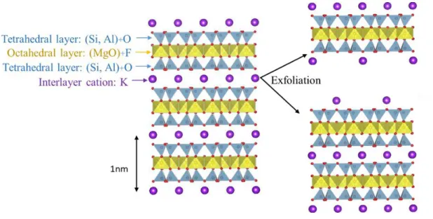
1.3 The Structure and Property of Mica
Mica is a type of phyllosilicates that exhibiting two-dimensional sheet or layered structure. Mica is formed by a complex aluminosilicate mineral with the ideal unit cell formula can be represented by a chemical formula of X2Y4-6Z8O20(OH,F)4, in which X represents interlayer cations (K+, Na+, Ca2+), Y represents the octahedral coordinated elements (Al3+, Mg2+, Fe2+, Li+ ,..), and Z represents the tetrahedral coordinated elements (Si4+, Al3+,..). Two tetrahedral (T) sheets on both sides of an octahedral (O) sheet forming the layered mica structural unit (1 nm). Silicate tetrahedron (SiO4) and aluminum octahedron (AlO6) are the basic building blocks of mica layers and these layers with a ratio of 2:1 are repeatedly bound together interlayer potassium ions. Mica layered structure is consist of alternating aluminosilicate and potassium ion layers. In the aluminosilicate layer Si ions are partially substituted by Al ions (1/3), which gives a net negative charge to the layer and interlayer cations (K+) maintaining the charge neutrality of the unit. For the phlogopite mica the center of each octahedron is occupied by Mg and for muscovite mica Al. The electrostatic force between the K+ and
5 the aluminosilicate layer is shared among 12 oxygen atoms, due to the weak attraction force between the K+ and the aluminosilicate layers and perfect cleavage parallel to the (001) plane occurs easily along this interface. Upon cleavage along (001) plane mica surface exhibits a hexagonal arrangement of Si and O atoms partly covered by potassium ions produces two large, atomically flat surfaces on both sides of the cleaved mica, with each expose surface is occupied with equal but randomly distributed K+ atoms to preserve the charge neutrality of the mica sheets.
Figure 1.2: Crystal structure. (a) Structural unit of mica. Surface structure of phlogopite mica: (b) [001] projection and (c) [100] projection.
The following are the most noticeable features that makes mica an ideal material for flexible device applications.
i. 2D structure: Mica shows strong intra-layer but weak inter-layer van der Waals (vdW) and electrostatic interactions that’s possible to peel off over layer from bulk mica creating two- dimensional thin film.
6 ii. Transparent: Several-layer mica sheet exhibits clear transmittance in the ultraviolet–visible-
infrared range of the electromagnetic spectrum and gain more attraction to optoelectronic applications.
iii. Elastic: The high elasticity of atomically thin mica nanosheets as a mechanical property of mica crystals validate their applicability as dielectric substrates in highly demanding mechanical applications.
iv. Flexible: Mica has very high yield strain and the bending radius down to 0.03 cm is reported for 100 nm thick mica sheet [29].
v. Chemically inert: The absence of dangling bonds on surface makes mica highly tolerable against chemical bonding.
vi. Electrically insulating: Insulating properties of mica is much higher than other 2D insulating materials and mica is a perfect candidate for the use as a gate dielectric in flexible electronic devices [29].
vii. High thermal resistance: artificially synthesized pure phlogopite mica (KMg3AlSi3O10F2), which is suitable for electronic device processes and applications because it is thermally stable up to a maximum operating temperature of ~1100 °C and is much purer than natural mica in minerals, e.g., muscovite (KAl2(AlSi3)O10(OH)2) with the temperature of ~550 °C [30].
Coefficient of thermal expansion (CTE) of mica matched with Si.
viii. Atomically flat surface: This is the key reason for using mica in TEM and AFM observations.
Moreover, mica is the ideal substrate because of its ultra-high surface flatness for investigating other 2D materials.
ix. Inexpensive and abundant: Phyllosilicates are one of the most abundant minerals found in in all the three major rock verities-igneous, sedimentary and metamorphic.
7
1.4 Remaining Chapter Summary
This thesis will focus on developing exfoliation method and characterizing layered materials phlogopite mica with AFM, SAM, and the focus electron beam induced etching. The results will be split into the following main chapters:
Chapter 2. Background- This chapter will give a background of all experimental technique used in this project.
Chapter 3. Mechanical exfoliations- Introducing new approach of mechanical exfoliations process with the poly-urethane hand roller. This chapter will discuss the mechanism and advantages of the newly invented approach to exfoliate wider and high quality nanosheets and compare the result with other conventional methods.
Chapter 4. Thickness measurement- The main objective of this chapter is to evaluate thickness of few layer mica nanosheets with Auger electron spectroscopy, SEM image observations and current- voltage characterizations of insulating few layer mica nanosheets are discussed.
Chapter 5. Electron beam irradiations- In this chapter we will investigate the effect and involving mechanism of focus electron beam irradiations on mica surface and finding the beam controlling parameters to selectively etching mica layers with the incident electron beam.
Chapter 6. Conclusions- This chapter will summarize the results found in this thesis and give insight into the future directions of these results.
References
1. Xia, Fengnian, et al. "Two-dimensional material nanophotonics." Nature Photonics 8.12 (2014):
899-907.
8 2. Novoselov, Kostya S., et al. "Two-dimensional gas of massless Dirac fermions in
graphene." Nature 438.7065 (2005): 197-200.
3. Kang, Jiahao, et al. "Graphene and beyond-graphene 2D crystals for next-generation green electronics." Micro-and Nanotechnology Sensors, Systems, and Applications VI. International Society for Optics and Photonics 9083. (2014): 908305-908312.
4. Castellanos-Gomez, Andres. "Why all the fuss about 2D semiconductors?" Nature Photonics 10.4 (2016): 202-204.
5. Bhimanapati, Ganesh R., et al. "Recent advances in two-dimensional materials beyond graphene." ACS nano 9.12 (2015): 11509-11539.
6. Song, Li, et al. "Large scale growth and characterization of atomic hexagonal boron nitride layers." Nano letters 10.8 (2010): 3209-3215.
7. Liu, Han, et al. "Phosphorene: an unexplored 2D semiconductor with a high hole mobility." ACS nano 8.4 (2014): 4033-4041.
8. Kumar, Anshuman, et al. "Tunable light–matter interaction and the role of hyperbolicity in graphene–hBN system." Nano letters 15.5 (2015): 3172-3180.
9. Fei, Ruixiang, and Li Yang. "Strain-engineering the anisotropic electrical conductance of few- layer black phosphorus." Nano letters 14.5 (2014): 2884-2889.
10. Li, Peining, et al. "Hyperbolic phonon-polaritons in boron nitride for near-field optical imaging and focusing." Nature communications 6.1 (2015): 1-9.
11. Dai, S., et al. "Tunable phonon polaritons in atomically thin van der Waals crystals of boron nitride." Science 343.6175 (2014): 1125-1129.
12. Novoselov, Kostya S., et al. "Electric field effect in atomically thin carbon films." science 306.5696 (2004): 666-669.
13. Dean, Cory R., et al. "Boron nitride substrates for high-quality graphene electronics." Nature nanotechnology 5.10 (2010): 722-726.
9 14. Jeong, S., et al. "Raman scattering studies of the lattice dynamics in layered MoS2." Journal of
the Korean Physical Society 66.10 (2015): 1575-1580.
15. Wilson, Jl A., and A. D. Yoffe. "The transition metal dichalcogenides discussion and interpretation of the observed optical, electrical and structural properties." Advances in Physics 18.73 (1969): 193-335.
16. Zhao, Yang, et al. "Recent developments and understanding of novel mixed transition‐metal oxides as anodes in lithium ion batteries." Advanced Energy Materials 6.8 (2016): 1502175- 1502194.
17. Kalantar-zadeh, Kourosh, et al. "Two dimensional and layered transition metal oxides." Applied Materials Today 5 (2016): 73-89.
18. Maslova, M. V., L. G. Gerasimova, and Willis Forsling. "Surface properties of cleaved mica." Colloid Journal 66.3 (2004): 322-328.
19. Castellanos‐Gomez, Andres, et al. "Atomically thin mica flakes and their application as ultrathin insulating substrates for graphene." Small 7.17 (2011): 2491-2497.
20. Low, Chong Guan, et al. "Graphene field effect transistors with mica as gate dielectric layers." Small 10.20 (2014): 4213-4218.
21. Bitla, Yugandhar, and Ying-Hao Chu. "MICAtronics: A new platform for flexible X- tronics." FlatChem 3 (2017): 26-42.
22. Rudenko, A. N., et al. "Graphene adhesion on mica: Role of surface morphology." Physical Review B 83.4 (2011): 045409.
23. Low, Chong Guan, and Qing Zhang. "Ultra‐thin and Flat Mica as Gate Dielectric Layers." Small 8.14 (2012): 2178-2183.
24. Barth, Johannes V., Giovanni Costantini, and Klaus Kern. "Engineering atomic and molecular nanostructures at surfaces." Nanoscience and technology: a collection of reviews from Nature journals. 2010. 67-75.
10 25. Utke, Ivo, Stanislav Moshkalev, and Phillip Russell, eds. Nanofabrication using focused ion and
electron beams: principles and applications. Oxford University Press (2012).
26. Pauling, Linus. "The structure of the chlorites." Proceedings of the National Academy of Sciences of the United States of America 16.9 (1930): 578-582.
27. Fleet, Michael E., et al., eds. "Rock-forming minerals: Micas." Geological Society of London (2003).
28. Castellanos-Gomez, Andres, et al. "Mechanical properties of freely suspended atomically thin dielectric layers of mica." Nano Research 5.8 (2012): 550-557.
29. He, Yudong, et al. "Mica, a Potential Two‐Dimensional‐Crystal Gate Insulator for Organic Field‐
Effect Transistors." Advanced Materials 23.46 (2011): 5502-5507.
30. Barlow, S. G., and D. A. C. Manning. "Influence of time and temperature on reactions and transformations of muscovite mica." British ceramic transactions 98.3 (1999): 122-126.
11
Chapter 2 Background
2.1 Atomic Force Microscopy
Atomic force microscopy (AFM) is an atomic resolution type of scanning probe microscopy (SPM), the illustrated resolution on the order of fractions of a nanometer, more than thousand times better than the optical diffraction limit [1]. The surface information of the sample is gathered by "feeling"
or "touching" the sample surface with a mechanical probe and building up a map of the height or topography of the surface as it goes along. Piezoelectric elements that facilitate tiny but accurate and precise movements on electronic command enable perfect scanning of the sample. Through this research work we have used Molecular Imaging’s PicoPlus controller, the PicoScan 2500 with the environmental chamber for the control environmental experiment.
Figure 2.1: AFM setup. [https://images.app.goo.gl/4zWEVPADUmmcTEv1A]
12 Figure 2.2: An AFM instrument generates topographic images by moving a small cantilever over the surface of a sample. A sharp tip is attached on the end of the cantilever that contact with the sample surface, the reflected laser beam from the backside of the cantilever is detected by a photodetector and send to the detector and feedback electronic.
The atomic force microscopy consists of cantilever with a tip, a laser source, photodiode with detector and feedback circuit. Typically, silicon or silicon nitride cantilever with a sharp tip (probe) attached at its end which is used to scan the specimen surface by contacting the sample surface or vibrating on top of the surface depending on the scan mode. When the tip is brought into proximity of a sample surface, forces between the tip and the sample lead to a deflection of the cantilever according to Hooke's law [2]. Depending on the scan mode, forces that are measured in AFM include mechanical contact force, van der Waals forces, capillary forces, chemical bonding, electrostatic forces etc. The AFM can be operated in a number of modes, depending on the application such as static (also called contact) modes and a variety of dynamic (non-contact or "tapping") modes where the cantilever is vibrated or oscillated at a given frequency [3]. In this research work we have used contact mode operations with the silicon nitride tip for the image topography and for the conductive AFM mode, we used 10 nm Iridium coated silicon nitride tips.
13 Figure 2.3: AFM beam-deflection detection
2.1.1 Conductive Atomic Force Microscopy
Atomic force microscopy has divers of functions to characterized surface morphology of different type of sample. With modifications of the setup, AFM can be used to measure the surface conductivity and tunneling current of two-dimensional materials. The conductive atomic force microscopy (cAFM) can simultaneously measure the topography of the sample surface and electric current flow at the contact point of the tip and sample. Laser deflection from the backside of the cantilever measured the topographic image of the sample, while current is detected using a current-to-voltage preamplifier [4]. The application of topographic imaging and current detection make C-AFM advanced scanning probe microscopy compared to scanning tunneling microscopy (STM). Generally, in STM the current flowing between the tip and the sample (the distance can be calculated depending on the current) constricting the topography picture of the sample. Therefore, when STM is performed a sample portion scanning, it is not possible to discern the current fluctuations that are related to a change in the topography (due to surface roughness) or to a change in the sample conductivity (due to intrinsic inhomogeneities). On the other hand, the C-AFM is generally operated in contact mode; the tip can
14 be kept at one location while the voltage and current signals are applied/read, or it can be moved to scan a specific region of the sample under a constant voltage (and the current is collected).
The conductive atomic force microscopy is operated under the following conditions: i) the tip (probe) must be conductive; ii) a voltage source is needed to apply a potential difference between the tip and the sample holder; iii) a pre-amplifier is used to convert the current signal into a voltage signal that can be read by the computer via an analog–digital converter [4]. In C-AFM experiments, the sample holder must needed to use conductive wire or tape to connect the sample with holder to make complete circuit to apply bias voltage [5]. The currents collected by the CAFM obey the relationship:
I = J × Aeff
where I is the total current flowing through the tip/sample nanojunction, J is the current density and Aeff is the effective emission area through which electrons can flow [4]. The most common mistake in C-AFM research is to assume that the effective emission area Aeff equals the physical contact area Ac. Usually this assumption is incorrect because in different tip/sample systems the electrical field applied may propagate laterally. For example, the lateral conductivity of the sample is very high when the C-AFM tip is placed on a metal, making the whole sample surface area electrically connected (Aeff equals the area covered by the metallic film/electrode) [6,7]. On the contrary, if the C-AFM tip is placed directly on an insulator, it acts as a nano-sized electrode and provides a very high lateral resolution. Aeff has been defined as: "the sum of all those infinitesimal spatial locations on the surface of the sample that are electrically connected to the C-AFM tip (potential difference is negligible).
2.2 Scanning Auger Microscopy
Scanning Auger microscopy (SAM)/Auger electron spectroscopy (AES) is an Auger electron effect- based electron beam techniques. An incident electron beam with energy typically 3–25 keV impinges
15 on sample surface and causes an Auger electrons emission. This is a chain of radiation-less transitions process following the ionization of atoms by the incident electrons and finally ends up by the ejection of an electron which is known as an Auger electron. Very short inelastic mean free paths of the Auger electron make AES extremely surface sensitive (sampling depth of 3–5 nm) thus allow the analysis of the elemental composition of materials.
The elemental maps of the sample surface are produced by scanning Auger microscopy by scanning the electron beam over the sample and selecting specific Auger peaks. Depth profiling can also be run by AES using an Ar+ sputter gun and in-depth elemental distributions are obtained through measurements of concentration profiles. The Auger depth profiling reveals ultra-thin layers and quantifying their elemental composition also in-depth information can also be obtained by analyzing a cross-sectional sample. In the SAM observations, sample preparations are quite convenient compared to transmission electron microscopy, complex sample preparation are not required in SAM.
Ultra-high surface sensitivity makes SAM complementary to electron microscopy techniques (EDX and EELS) and higher spatial resolution offers an alternative to photoelectron spectromicroscopy (XPEEM).
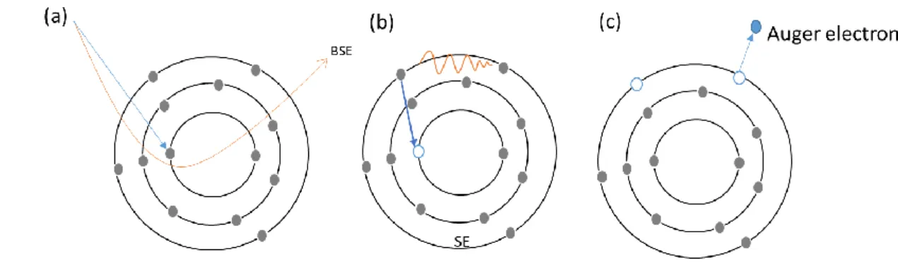
In the process of Auger effect, an atom is excited by a beam of electrons with energies in the range of several eV to 50 keV, a core state electron can be removed leaving behind a hole. Leaving one electron from the core level transfer the atom into unstable state, the core hole can be filled by an outer shell electron, whereas the electron moving to the lower energy level loses an amount of energy equivalent to the difference in orbital energies. The transition energy can be coupled to a second outer shell electron, which will be ejected from the atom if the transferred energy is larger than the orbital binding energy [8-13].
The emitted electron will have a kinetic energy of:
Ekin = ECore State – EB – E`C,
16 where ECore State is the core level, EB is first outer shell and E`C is second outer shell electron positive binding energies. Since a specific atom has unique orbital energies, analysis of the emitted electrons can provide information about the chemical composition of a surface. Figure 2.4 illustrates two schematic views of the Auger process.
Figure 2.4: (a) The incident electron makes the ionization of the core level electron in the atom. (b) Upper level electron falls to a lower level by releasing a quantum of energy and (c) the energy released from the second electron excites the Auger electron which leaves the atom.
The surface sensitivity in AES involved with emitted electrons which usually have energies ranging from 50 eV to 3 keV and at these values, in the solid electrons have a short mean free path. The electrons escape depth is therefore localized within a range few nanometers depth of the target surface (Fig. 2.5), this give AES an extreme sensitivity to surface species [13]. Ultra-high vacuum (UHV) conditions is required in the AES setup because of the low energy of the Auger electrons.
Measurement in high vacuum conditions prevent electron scattering [12–14]. Typical AES setup schematically shown in Fig. 2.6. In this configuration, incident focused electrons strike on a sample and emitted electrons (Auger electrons) are deflected into a cylindrical mirror analyzer (CMA). The collected Auger electrons in the electron energy analyzer are plotted as a function of energy against the broad secondary electron background spectrum [15].
17 Figure 2.5: Auger electron fail to emerge with their characteristic energies if they start from deeper than about 0.5 to 5 nm into the surface.
Figure 2.6: AES experimental setup using a cylindrical mirror analyzer (CMA).
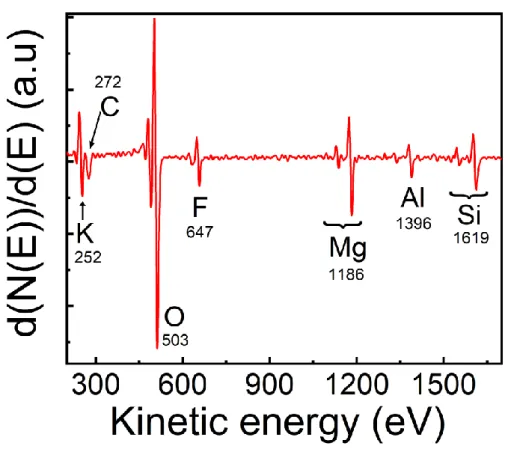
18 In the collecting AES spectra, the Auger peaks intensity is small compared to the background noise level, to highlight the actual peak intensities of specific elements AES is often run in a derivative mode by modulating the electron collection current via a small applied AC voltage. Derivative mode of AES spectra emphasizes Auger fine structure with small secondary peaks surrounding the primary Auger peak. Figure 2.7 illustrates a derivative spectrum from a mica sample clearly showing the Auger peaks.
Figure 2.7: Auger spectrum of mica in derivative mode plotted as a function of Auger electron energy.
2.3 Inelastic Mean Free Path
The term inelastic mean free path (IMFP) are frequently used to specify the surface sensitivity of Auger-electron spectroscopy. The IMFP is define as how far an electron on average travels through a solid before losing its energy. When a monochromatic primary electrons beam is incident on a
19 sample surface, Auger electrons from atoms near-surface region of the solid are ejected. Through plasmon excitation, electron-hole pair formation, and vibrational excitation majority of incident electron loss their primary energy when passing through the solid sample surface [16].
The intensity of the primary electron beam I0 damps as a function of distance d into the solid. The intensity decay can be expressed as follows:
I(d) = I0 e-d/ λ(E)
Where I(d) is the intensity after the primary electron beam has traveled through the solid to a distance d. The parameter λ(E), termed the inelastic mean free path (IMFP), is defined as the distance an electron beam can travel before its intensity decays to 1/e of its initial value. The inelastic mean free path of electrons can roughly be described by a universal curve that is the same for all materials [17,18].
Figure 2.8: Universal curve for the electron inelastic mean free path in elements in [17].
20
2.4 Tunneling
2.4.1 Metal-Insulator-Metal Tunnel Diode
Figure 2.9: Energy-band diagrams of MIM structures. (a) Symmetrical MIM under equilibrium. (b) Under bias, V> Ø0. (c) Asymmetrical MIM.
A metal-insulator-metal (MIM) tunnel diode is a thin-film structure consisting of well-defined single crystal material sandwiched between two metal electrodes is the ideal model for study of tunneling current of insulating materials. In the MIM structure the electrons from the first metal can tunnel through the insulator film and be collected by the second metal. It displays nonlinear I-V characteristics but negative resistance is not present. The nonlinear I-V nature is sometimes used for microwave detection as a mixer. Figures 2.9 (a) and (b) show the basic energy-band diagrams of a MIM diode with similar metal electrodes. Since all of the voltage applied is dropped across the insulator, the tunneling current through the insulator is,
𝐽 =4𝜋𝑞𝑚∗
ℎ3 ∬ 𝑇𝑡[𝐹(𝐸) − 𝐹(𝐸 + 𝑞𝑉)]𝑑𝐸⊥𝑑𝐸 At 0 K,
21 𝐽 = 𝐽0[∅̂ exp (−𝐶√∅̂) − (∅̂ + 𝑉) exp (−𝐶√∅̂ + 𝑉)],
where
𝐽0 ≡ 𝑞2
2𝜋ℎ𝑑∗2 and 𝐶 ≡4𝜋𝑑∗√2𝑚∗𝑞
ℎ
For the ideal symmetrical MIM structure the current density is given by
𝐽 = 𝐽0[(∅0−𝑉
2) 𝑒𝑥𝑝 (−𝐶√∅0−𝑉
2) − (∅0+𝑉
2) 𝑒𝑥𝑝 (−𝐶√∅0+𝑉 2)].
The present investigation we fabricating iridium-mica-iridium structure and measuring the tunneling properties of few-layer mica nanosheets using above equations with conductive atomic force microscopy.
References
1. Cappella, Brunero, and Giovanni Dietler. "Force-distance curves by atomic force microscopy." Surface science reports 34.1-3 (1999): 1-104.
2. Cappella, Brunero. "Physical Principles of Force–Distance Curves by Atomic Force Microscopy." Mechanical Properties of Polymers Measured through AFM Force-Distance Curves. Springer, Cham, (2016).
3. Binnig, Gerd, Calvin F. Quate, and Ch Gerber. "Atomic force microscope." Physical review letters 56.9 (1986): 930-933.
4. Lanza, Mario Conductive Atomic Force Microscopy. Berlin, Germany: Wiley-VCH (2017).
5. Murrell, M. P., et al. "Spatially resolved electrical measurements of SiO2 gate oxides using atomic force microscopy." Applied physics letters 62.7 (1993): 786-788.
22 6. Rommel, Mathias, et al. "Influence of parasitic capacitances on conductive AFM IV measurements and approaches for its reduction." Journal of Vacuum Science & Technology B, Nanotechnology and Microelectronics: Materials, Processing, Measurement, and Phenomena 31.1 (2013): 01A108.
7. Yanev, V., et al. "Comparative study between conventional macroscopic IV techniques and advanced AFM based methods for electrical characterization of dielectrics at the nanoscale." Microelectronic engineering 86.7-9 (2009): 1911-1914.
8. Carlson, Thomas. Photoelectron and Auger spectroscopy. Springer Science & Business Media, 2013.
9. Briggs, David. "Practical surface analysis." Auger and X-Ray Photoelecton Spectroscopy 1 (1990): 151-152.
10. Bialkowski, Stephen E. Photothermal spectroscopy methods for chemical analysis. Vol. 177.
John Wiley & Sons (1996).
11. Hofmann, S. "Characterization of nitride coatings by Auger electron spectroscopy and x‐ray photoelectron spectroscopy." Journal of Vacuum Science & Technology A: Vacuum, Surfaces, and Films 4.6 (1986): 2789-2796.
12. Feldman, Leonard C., and James W. Mayer. "Fundamentals of surface and thin film analysis." North Holland, Elsevier Science Publishers, Amsterdam, The Netherlands (1986).
13. Oura, K., et al. "M. Katayama M." Surface Science: An Introduction” Springer, Berlin (2003).
14. Kittel, Charles, Paul McEuen, and Paul McEuen. Introduction to solid state physics. Vol. 8. New York: Wiley (1996).
15. Palmberg, Paul William. Handbook of Auger electron spectroscopy: a reference book of standard data for identification and interpretation of Auger electron spectroscopy data. Physical Electronics Industries (1972).
23 16. Seah, M. Pl, and W. A. Dench. "Quantitative electron spectroscopy of surfaces: A standard data base for electron inelastic mean free paths in solids." Surface and interface analysis 1.1 (1979):
2-11.
17. Egerton, Ray F. Electron energy-loss spectroscopy in the electron microscope. Springer Science
& Business Media (2011).
18. Werner, Wolfgang SM. "Electron transport in solids for quantitative surface analysis." Surface and Interface Analysis: An International Journal devoted to the development and application of techniques for the analysis of surfaces, interfaces and thin films 31.3 (2001): 141-176.
24
Chapter 3
Exfoliation of large-area high-quality two-dimensional mica nanosheets on substrate
Mechanical exfoliations and transfer techniques led to understanding of novel physical phenomena of two-dimensional (2D) materials. The original exfoliation method, which remained largely unchanged during the past decade, provides relatively small flakes with moderate yield. Here, we present a conventional approach to exfoliate single-layer or few-layer nanosheets from cleavable layered crystals using a polyurethane hand roller. The sample was a single-crystal oxide of pure artificially-synthesized phlogopite (KMg3AlSi3O10F2), one of mica family. The mica nanosheets with high-quality were extended to more than 100-µm width on Si substrates. The nanosheets down to a single layer (1 nm) were characterized by atomic force microscopy (AFM), and elemental analysis was performed by scanning Auger electron spectroscopy/microscopy (SAM). The preparation of atomically thin insulating crystalline mica sheets will enable the fabrication of ultrathin, defect-free insulating substrates, dielectric barriers, or planar electron-tunneling junction.
Figure 3: Transferring process of mica nanosheets
3.1 Introduction
The perfection and physical properties of atomically thin two-dimensional (2D) materials are extremely sensitive to their synthesis and growth process. Achieving desired characteristics such as structural uniformity, high carrier mobility, tunable bandgap, and flexibility is the main challenge for
25 the synthesis and growth of next generation 2D materials. A reliable and optimized growth and manufacturing process is essential for the synthesis of 2D materials with uniform properties for the application in flexible and transparent optoelectronics. Scalable growth techniques such as chemical vapor deposition (CVD) and atomic layer deposition techniques have been used to grow large-area 2D materials such as graphene, [1–5] MoS2, [6,7] WS2 [8], and others [9–11] on different substrates.
But the development of CVD optimized growth approaches has proven to be a time-consuming process, since phenomena such as the formation of defects [4,12] and grain boundaries [13] happened during the growth process.
To prepare high-quality 2D materials, mechanical exfoliation processes are often performed, leading to understanding of their remarkable physical phenomena [14–21]. Mechanical exfoliation of monolayer or few-layer nanosheets from layered bulk crystals has played a central role to the rapidly accessing of high-quality flakes for exploring novel materials systems. For example, nearly all of the novel properties of graphene were first discovered and measured on mechanically exfoliated flakes [22–24] and other 2D materials such as h-BN, MoS2 and SnS2 have gained large attention due to their distinctive properties [25–27]. Also, it can be expected that the exfoliation process will continue to play a prominent role in the development of 2D materials.
The single-crystalline layered structure of pure artificially synthesized phlogopite mica, a phyllosilicate mineral with oxides of aluminum (Al) and magnesium (Mg), and potassium (K) and fluorine (F) in the chemical formula of KMg3AlSi3O10F2 makes this material a promising candidate to produce atomically thin insulating crystals by mechanical exfoliation. Moreover, due to its mechanical properties, high dielectric constant, and high resistance to heat, water, and chemical agents, bulk mica has already been extensively used in the electronic industry in many applications as a substrate, heat and electrical insulator, or dielectric barrier. Recently, bulk mica has been also employed as a substrate to fabricate ultra-flat graphene samples [28–33]. The 2D nature of these atomically thin crystalline insulator sheets makes them very interesting candidates in applications
26 such as insulating barriers in planar tunnel junctions or as flexible substrates for graphene or molecular electronic devices [34–38]. For development of high-quality nanoscale devices, conventional and reliable methods to extend the areal size of 2D mica nanosheets are required, as well as methods to precisely characterize their thickness and chemical components. In this work, we report a mechanical exfoliation process to prepare wider atomically thin mica nanosheets down to one layer (1 nm) on SiO2/Si, Au/Si, and Ir/Si substrate. A combined characterization of these nanosheets by quantitative optical microscopy and atomic force microscopy (AFM) are presented.
We also performed Auger electron spectroscopic (AES) analysis to compare the carbon contaminations on the mica nanosheets prepared in our modified exfoliation process to those prepared with other commonly used mechanical exfoliation technique.
3.2 Experimental Methods
In order to mechanically exfoliate nanosheets from the bulk phlogopite and affix them to the substrates, we first adopted a tool in the exfoliation process, where Scotch tape have been widely used to exfoliate flakes from graphene and other 2D materials. Instead of Scotch tape, we used the tool of a clean polyurethane hand roller with a diameter of 20 mm; this is originally a commercial tool to remove dust from flat surfaces in semiconductor processes without residues (Semiconductive gel roller, EX215-AS, EXSEAL Co., Ltd., Mino, Japan). The viscosity of polyurethane is similar to that of poly-dimethylsiloxane (PDMS) and Scotch tape, but the polyurethane gives lower levels of residues. The outline of the mechanical exfoliation and affixing processes is shown in Fig. 3.1. First, the roller was rolled once over the top surface of the bulk mica to thinly exfoliate the surface, and the exfoliated mica sheets were attached to the surface of the roller. Subsequently, the roller was rolled over a substrate so that the sheets on the roller were transferred to the target area on the substrate.
The curved surface of the roller was suitable for separating thin mica sheets from the bulk mica and transferring them onto the substrate. To compare the performance of the roller, we also used a PDMS
27 stamp with a thickness of 0.5 mm to exfoliate the mica nanosheets. For the substrates, we used native oxidized Si wafers (SiO2/Si) and Si wafers coated with gold (Au/Si) or iridium (Ir/Si) at a thickness of about 10 nm. Before transferring the mica sheets onto the substrate, the SiO2/Si substrate is ultrasonically cleaned in acetone, and mill-Q water, and then subjected to ozone cleaning to remove ambient hydrocarbon adsorbates from its surface. We heated the substrate for few minutes at 250 °C in air on a conventional laboratory hotplate to evaporate water molecules from the surface of the substrate. Using the poly-urethane hand roller technique, mica nanosheets with thicknesses ranging from hundreds of nanometers down to just one nanometer, corresponding to one layer of the mica, were produced. When mica is mechanically exfoliated, cleavage occurs along the (001) basal plane of a K atom layer (Fig. 3.2). As a result, approximately half of the K atoms randomly remain on the surface of the exfoliated mica sheet, while the other half remain on the counter surface of the mica crystal. Inspection by optical microscopy and AFM shows the successful transfer of single and few- layer wide area mica nanosheets on different substrates.
28 Figure 3.1: Outline of the mechanical exfoliation and affixing process to prepare the 2D mica nanosheets onto the substrate. First, a polyurethane hand roller is rolled over the mica. Subsequently, the exfoliated mica nanosheets on the surface of the roller are transferred and affixed to the substrate by rolling the roller over the substrate. [39]
29 Figure 3.2: Atomistic model of phlogopite (KMg3AlSi3O10F2) viewed along the basal plane. The grayish blue polygons are the tetrahedrons composed of Al, Si, and O, where Al and Si atoms exist at a ratio of 1:3. The yellow polygons are the octahedrons composed of Mg, O, and F. The small red spheres denote O atoms at the sites that are connected to the tetrahedrons, and partly F atoms at the sites that are not connected to the tetrahedrons. The large purple spheres denote K atoms. The separation between the K layers is approximately 1.0 nm, which is the unit of thickness of mechanically cleaved phlogopite. [39]
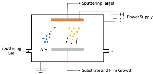
For the gold (Au/Si) or iridium (Ir/Si) substrates, we used native oxidized Si wafers (SiO2/Si) coated with gold (Au) or iridium (Ir) at a thickness of about 10 nm deposited by DC magnetron sputtering.
Figure 3.3 shows the schematic of the sputtering coating. DC magnetron sputtering coat was conducted in a vacuum chamber with an argon (Ar) gas (99.999%) pressure of 6 Pa at a discharge current of 15 mA with a DC power supply.
30 Figure 3.3: Schematic of the DC magnetron stuttering.
3.3 Results and Discussion
Figure 3.4 shows some optical microscopy images of mica nanosheets transferred onto two Si substrates with a 300 nm and a 10 nm SiO2 thickness. The mica nanosheets on the Si substrate with the 300 nm SiO2 thickness were more enhanced in contrast, as shown in Fig. 3.4(a,b), compared with those on the Si substrate with the thinner oxide. We were able to clearly observe down to one-layer mica nanosheets on the Si substrate, whereas on the 10 nm SiO2/Si substrate, down to five-layer mica nanosheets were recognized, as shown in Fig. 3.4(c,d) . The sizes of nanosheets in Figs. 3.4(b) and (d) were about 850 µm × 350 μm with 6 layers and about 1200 µm × 800 μm with 10 layers, respectively. Our modified approach can make it easier to obtain large-area mica nanosheets.
31 Figure 3.4: Optical microscopy images of mica nanosheets deposited on SiO2/Si substrates. The color and contrast difference over the nanosheets correspond to different thicknesses of the mica nanosheets.
(a) Mica nanosheets with thicknesses ranging from 1 to 20 nm on the 300 nm SiO2 /Si substrate. (b) Larger area 6 layers (6 nm) mica nanosheets on the 300 nm SiO2/Si substrate. (c) Four to several layers and (d) 10 layers extended area of mica nanosheets on a 10 nm SiO2/Si substrate.
AFM imaging would provide an independent measurement of the thickness and morphology of 2D materials. The typical contact-mode topographic AFM images of mica nanosheets on the SiO2/Si substrates are shown in Figs. 3.5 (a) and (b), and those on the Au-coated Si (Au/Si) and the Ir-coated Si (Ir/Si) substrates are shown in Figs. 3.5 (c) and (d), respectively. To evaluate their thicknesses, we examined the cross-sectional profiles through the boundary between the SiO2 surface and the mica nanosheets in the respective images, as shown below the AFM images. The minimum height
32 differences between the substrate and the mica nanosheets in Figs. 3.5 (a) and (b) were 1 and 5 nm, corresponding to one- and five-layer mica, respectively. Although the dimensions of single layer mica nanosheets fabricated by mechanical exfoliation processes, such as with Scotch tape, are usually not much larger than 1 µm × 1 µm, we were able to prepare single layer mica nanosheets with dimensions of ~10 µm ×10 µm using the polyurethane hand roller (Fig. 3.5 (a)). The dimensions of the five-layer thick mica nanosheets reached to several hundredth µm in width (Fig. 3.5 (b)). We also observed few layers mica nanosheets with larger area on the Au/Si and Ir/Si substrate (Figs. 3.5 (c) and (d).
Figure 3.5: AFM images of mica nanosheets mechanically exfoliated to (a) 1 nm and (b) 5 nm thickness, affixed on the SiO2/Si substrates. AFM images of several layer mica nanosheets on (c)
33 Au/Si and (d) Ir/Si substrates. The typical cross-sectional line profiles along the lines in the images are shown below the images in (a) and (b). The numerals with the character “L” indicate the thickness of the mica nanosheets in the unit of one mica layer (1 nm) measured from the cross-sectional line profiles. [39]
It should be noted that the mica nanosheets often showed ripples and wrinkles, probably because of formation of water bubbles between the nanosheet and substrate. In our experiment, we found that monolayer or bilayers mica showed ripple because of existing water molecules between the thin mica and the substrate. Thus, we heated the substrates before transferring the mica nanosheets, resulting in smooth mica nanosheets without ripples and wrinkles, as shown in Fig. 3.6.
Figure 3.6: Bilayer mica nanosheets transfer on SiO2/Si substrate (a) with and (b) without performing heating treatment at 2500C for few minutes of the substrate before transferring mica on it. [39]
To examine the cleanliness of mica nanosheets exfoliated with our modified process, we performed the AES analysis of mica nanosheet surfaces (the details of the AES analysis are explained in the next chapter). From the AES spectra, we observed all the mica elements with detecting CKLL Auger peaks at 272 eV close to the KLMM peaks at 252 eV, as shown in Fig. 3.7 (a). The degree of carbon contamination depends on the preparation method [40-44]. The AES spectra around the CKLL peaks
34 of 10-layer-thick mica nanosheets on the Au/Si substrate prepared using the polyurethane hand roller and a stamp of a thin PDMS sheet are shown in Fig. 3.7 (b). The carbon peak intensities were higher for the mica nanosheets exfoliated with the PDMS stamp. This tendency of the difference in the C peaks using the two different tools was confirmed for other mica nanosheet samples. This suggests that the higher carbon amount originated from the surface of the PDMS stamp. PDMS contains uncross-linked dimethylsiloxane oligomers, which are known to be present on its surface [40,42].
Although the polyurethane hand roller did not contain these undesirable species, the carbon peak did not disappear, which was possibly attributed to contamination from the laboratory environment during the process as we performed the exfoliation process in air.
35 Figure 3.7: (a) AES spectra of 10-layer-thick mica nanosheets on the SiO2/Si substrate. The peaks denoted by the element symbols are the mica elements except C peaks at 272 eV. The C peaks were subjected to hydrocarbonous contaminations on the sample surface. (b) AES spectra to compare the difference in the contamination on the nanosheets prepared with the polyurethane hand roller (red) and the PDMS stamp (black). [39]
36 It is widely known that mica has a layered structure with the potassium (K) ion layers sandwiched between aluminosilicate layers. The aluminosilicate layer, which is a negatively charged oxide layer because of the substitution of a quarter of the Si4+ ions by Al3+ ions, is bounded together electrostatically with a layer of K+ atoms, as shown in the model of Fig. 3.2. Since the attractive force between the K+ layers and the aluminosilicate layers are weak, cleavage occurs easily along their interface. On the other hand, the interactions between the mica surface and the Si substrate during exfoliation are van der Waals forces. Exfoliation of mica sheets on the Si substrate represents a competition between the weak electrostatic force at the K+ layer and the van der Waals forces between the bottom surface of mica sheet and the surface of the Si substrate, which are facing each other.
When the adhesive force between the bottom of the mica sheet and the substrate exceeds the force between the mica layers, the mica sheet can be separated from the layered mica, leaving the thin mica nanosheet on the substrate surface. Figure 3.8 gives a schematic diagram of the key steps of modified mica exfoliation process, and illustrates how the solid curve surface of the poly-urethane hand roller can increase the interaction at the mica/substrate interface and thus enhance the exfoliation process.
When the roller together with few layers mica on its surface is pressed over the substrate, more uniform contact is established between the outermost mica layer and the support substrate which increased van der Waals force driven by an increase in pressure at the interface. The roller increases the force between mica and substrate surface by establishing pressure difference, increased contact area, and decreased overall contact distance. As a result, when the roller is rolled, separations occurred between the mica layers and monolayers or few layers of mica is transferred from the roller surface onto substrate surface. Similar mechanism happened when the roller is rolled over the bulk mica to transfer mica sheets onto the roller surface. Sometimes monolayer or few layers mica flakes that attached on the roller surfaces from the bulk mica are transferred onto the substrate surface directly. Upon cleavage of mica surface exhibits a hexagonal arrangement of Si (1/4 Al substitution) and O atoms partly covered by potassium ions over the exposing surface [45].
37 Figure 3.8: Key steps of the modified exfoliation process for 2D materials. (a) Increased pressure by the roller causes a small and uniform spacing between mica and substrate which in turn enhances the van der Waals interaction at the interface. (b) Separation between the mica layers occurred as the roller is started to rolling over the substrate.
3.4 Conclusion
We have successfully deposited atomically thin nanosheets of phlogopite mica with thickness down to a single layer (1 nm) and few layers with an area of several hundredth square micrometers on SiO2/Si, Au/Si, and Ir/Si substrates. Mechanical exfoliation of mica nanosheets with a clean polyurethane roller can easily provide large area mica nanosheets. The AES analysis demonstrated that our modified exfoliations mica had a low level of hydrocarbon contamination compared with the commonly used PDMS exfoliations process. We suggest that the exfoliation approach demonstrated here is applicable to a wide range of 2D materials. Hence, our conventional method possibly accelerates the exploration of new 2D materials by providing an efficient pathway to large nanosheets derived from layered crystals via exfoliation.
38
References
1. Bhaviripudi, Sreekar, et al. "Role of kinetic factors in chemical vapor deposition synthesis of uniform large area graphene using copper catalyst." Nano letters 10.10 (2010): 4128-4133.
2. Sutter, E., P. Albrecht, and P. J. A. P. L. Sutter. "Graphene growth on polycrystalline Ru thin films." Applied Physics Letters 95.13 (2009): 133109.
3. Sutter, P. W., P. M. Albrecht, and E. A. Sutter. "Graphene growth on epitaxial Ru thin films on sapphire." Applied Physics Letters 97.21 (2010): 213101-213103.
4. Virojanadara, Chariya, et al. "Homogeneous large-area graphene layer growth on 6 H-SiC (0001)." Physical Review B 78.24 (2008): 245403-245408.
5. Ge, Wanyin, et al. "Large-scale synthesis of NbS2 nanosheets with controlled orientation on graphene by ambient pressure CVD." Nanoscale 5.13 (2013): 5773-5778.
6. Wang, Shanshan, et al. "Shape evolution of monolayer MoS2 crystals grown by chemical vapor deposition." Chemistry of Materials 26.22 (2014): 6371-6379.
7. Wang, Xinsheng, et al. "Controlled synthesis of highly crystalline MoS2 flakes by chemical vapor deposition." Journal of the American Chemical Society 135.14 (2013): 5304-5307.
8. Zhang, Yu, et al. "Controlled growth of high-quality monolayer WS2 layers on sapphire and imaging its grain boundary." ACS nano 7.10 (2013): 8963-8971.
9. Huang, Jing-Kai, et al. "Large-area synthesis of highly crystalline WSe2 monolayers and device applications." ACS nano 8.1 (2014): 923-930.
10. Lu, Xin, et al. "Large-area synthesis of monolayer and few-layer MoSe2 films on SiO2 substrates." Nano letters 14.5 (2014): 2419-2425.
11. Brent, Jack R., Nicky Savjani, and Paul O'Brien. "Synthetic approaches to two-dimensional transition metal dichalcogenide nanosheets." Progress in Materials Science 89 (2017): 411-478.
12. Colombo, Luigi, et al. "Growth kinetics and defects of CVD graphene on Cu." EC Transactions 28.5 (2010): 109-114.
39 13. Huang, Pinshane Y., et al. "Grains and grain boundaries in single-layer graphene atomic
patchwork quilts." Nature 469.7330 (2011): 389-392.
14. Novoselov, Kostya S., et al. "Electric field effect in atomically thin carbon films." science 306.5696 (2004): 666-669.
15. Levendorf, Mark P., et al. "Graphene and boron nitride lateral heterostructures for atomically thin circuitry." Nature 488.7413 (2012): 627-632.
16. Radisavljevic, Branimir, et al. "Single-layer MoS2 transistors." Nature nanotechnology 6.3 (2011):
147-150.
17. Novoselov, Kostya S., et al. "Two-dimensional gas of massless Dirac fermions in graphene." nature 438.7065 (2005): 197-200.
18. Wei, Xiaoding, et al. "Recoverable slippage mechanism in multilayer graphene leads to repeatable energy dissipation." ACS nano 10.2 (2016): 1820-1828.
19. Nair, Rahul Raveendran, et al. "Fine structure constant defines visual transparency of graphene." Science 320.5881 (2008): 1308-1308.
20. Schedin, Fredrik, et al. "Detection of individual gas molecules adsorbed on graphene." Nature materials 6.9 (2007): 652-655.
21. Withers, Freddie, et al. "Electron transport of WS2 transistors in a hexagonal boron nitride dielectric environment." Scientific reports 4 (2014): 4967-4971.
22. Zhang, Yuanbo, et al. "Experimental observation of the quantum Hall effect and Berry's phase in graphene." nature 438.7065 (2005): 201-204.
23. Masubuchi, S., et al. "Observation of quantum Hall effect in mono-and bi-layer graphene using pulse magnet." Journal of Physics: Conference Series. Vol. 334. No. 1. IOP Publishing, 2011.
24. Ferrari, Andrea C., et al. "Raman spectrum of graphene and graphene layers." Physical review letters 97.18 (2006): 187401-187403.
25. Lee, Gwan-Hyoung, et al. "Flexible and transparent MoS2 field-effect transistors on hexagonal boron nitride-graphene heterostructures." ACS nano 7.9 (2013): 7931-7936.
40 26. Mak, Kin Fai, et al. "Atomically thin MoS2: a new direct-gap semiconductor." Physical review
letters 105.13 (2010): 136805-136809.
27. Strait, Jared H., Parinita Nene, and Farhan Rana. "High intrinsic mobility and ultrafast carrier dynamics in multilayer metal-dichalcogenide MoS2." Physical Review B 90.24 (2014): 245402- 245411.
28. Lui, Chun Hung, et al. "Ultraflat graphene." Nature 462.7271 (2009): 339-341.
29. Geringer, V., et al. "Intrinsic and extrinsic corrugation of monolayer graphene deposited on SiO2." Physical review letters 102.7 (2009): 076102-076106.
30. Meyer, Jannik C., et al. "The structure of suspended graphene sheets." Nature 446.7131 (2007):
60-63.
31. Teague, M. L., et al. "Evidence for strain-induced local conductance modulations in single-layer graphene on SiO2." Nano letters 9.7 (2009): 2542-2546.
32. Castellanos-Gomez, Andres, Nicolas Agraït, and Gabino Rubio-Bollinger. "Dynamics of quartz tuning fork force sensors used in scanning probe microscopy." Nanotechnology 20.21 (2009):
215502-215566.
33. Ponomarenko, L. A., et al. "Effect of a high-κ environment on charge carrier mobility in graphene." Physical review letters 102.20 (2009): 206603-206607.
34. Castellanos‐Gomez, Andres, et al. "Atomically thin mica flakes and their application as ultrathin insulating substrates for graphene." Small 7.17 (2011): 2491-2497.
35. Low, Chong Guan, et al. "Graphene field effect transistors with mica as gate dielectric layers." Small 10.20 (2014): 4213-4218.
36. Bitla, Yugandhar, and Ying-Hao Chu. "MICAtronics: A new platform for flexible X- tronics." FlatChem 3 (2017): 26-42.
37. Rudenko, A. N., et al. "Graphene adhesion on mica: Role of surface morphology." Physical Review B 83.4 (2011): 045409-045415.
![Figure 1.2: Crystal structure. (a) Structural unit of mica. Surface structure of phlogopite mica: (b) [001] projection and (c) [100] projection](https://thumb-ap.123doks.com/thumbv2/123deta/6150290.1081711/12.892.128.768.375.789/crystal-structure-structural-surface-structure-phlogopite-projection-projection.webp)
![Figure 2.1: AFM setup. [https://images.app.goo.gl/4zWEVPADUmmcTEv1A]](https://thumb-ap.123doks.com/thumbv2/123deta/6150290.1081711/18.892.119.768.628.829/figure-afm-setup-https-images-app-goo-zwevpadummctev.webp)

![Figure 2.8: Universal curve for the electron inelastic mean free path in elements in [17]](https://thumb-ap.123doks.com/thumbv2/123deta/6150290.1081711/26.892.227.658.607.858/figure-universal-curve-electron-inelastic-mean-free-elements.webp)