INVITED PAPER
Joint Special Section on Opto-electronics and Communications for Future Optical NetworkDevelopment of Low Loss Ultra-High ∆ ZrO 2 -SiO 2 PLC for Next Generation Compact and High-Density Integrated Devices
Masanori TAKAHASHI†,Nonmember, Yasuyoshi UCHIDA†,Member, Shintaro YAMASAKI†,Nonmember, Junichi HASEGAWA†,andTakeshi YAGI†,Members
SUMMARY For next generation planar lightwave circuit (PLC) de- vices, high function and high-density integration are required as well as downsizing and cost reduction. To realize these needs, high refractive in- dex difference between a core and a clad (∆) is required. To use PLC for practical applications, silica-based PLC is one of the most attractive candi- date. However, degradation of the optical properties and productivity occur when∆of the core becomes high. Thus,∆of most of the conventional PLC with GeO2-SiO2core is designed less than 2.5%. In this paper, we report a silica-based ultra-high∆PLC with ZrO2-SiO2core. 5.5%-∆ZrO2-SiO2
PLC has been realized with low propagation loss and basic characteristics has been confirmed. Potential of chip size reduction of the ZrO2-SiO2PLC is shown.
key words:integrated optics, MMI coupler, optical communication, optical device, planar lightwave circuit
1. Introduction
For next generation planar lightwave circuit (PLC) devices, high function and high-density integration are required as well as downsizing and cost reduction. To realize these fea- tures, in general, high refractive index difference between a core and a clad (∆) is required. Various devices employing core design with high∆have already been reported, such as silica glass PLC, SiON, InP, and Si based waveguides [1]–
[5]. However, high ∆waveguides generally cause degra- dation both optical performance and productivity. Espe- cially, low propagation loss and low coupling loss to single mode fibers (SMF) are necessary for practical applications, and productivity is also important. All these technologies have advantages and disadvantages. The InP waveguide is smaller than the silica PLC, and the Si wire waveguide is the smallest platform among these materials, and these materi- als are advantageous for high-density integration. However, high propagation loss and connection loss to SMF become problem. On the other hand, the silica PLC has various ad- vantages such as extremely low propagation loss, low con- nection loss to SMF, and established productivity. To take these advantages into account, the silica PLC is the most promising material if downsizing of the chip is realized.
In this paper, we report development of the silica-based high∆PLC to realize downsizing of the chip. Ultra-high
∆PLC is realized by employing ZrO2 as a dopant of the core, and the chip size is reduced drastically. We discuss
Manuscript received November 14, 2013.
Manuscript revised February 7, 2014.
†The authors are with Furukawa Electric Co., Ltd., Ichihara, 290-8555 Japan.
DOI: 10.1587/transele.E97.C.725
feasibility of the ZrO2-SiO2PLC to use next generation PLC devices though fine characteristics of the PLC.
2. Design of Ultra-High∆PLC
A PLC has the structure where light transmits the core em- bedded to the inside of the clad deposited on a Si substrate.
To confine the light in the core, refractive index of the core (ncore) needs to be designed higher than that of the clad (nclad), and the light is confined in the core by reflection at the boundary between the core and the clad. Since a chip size of the PLC is mainly determined by a minimum bend- ing radius (rmin) of the waveguide, it is effective to reduce rmin. In order to make rmin small, it is necessary to confine the light strongly in the core by raising∆. Therefore, it is necessary to raise∆to reduce chip size.
In the conventional PLC, GeO2is doped to the core to raise the ncore higher than nclad. In order to realize higher ncore, it is necessary to increase concentration of GeO2. However, if the concentration of GeO2 is increased, degra- dation of the optical performance and productivity of the PLC occur [1]. Thus, ∆of the most of the conventional PLC is designed less than 2.5%.
2.1 Required∆for next generation PLC
Target∆of the next generation PLC to realize downsizing of the chip and high-density integration is investigated. Re- lationships between rmin of the waveguide and ∆are cal- culated by beam propagation method (BPM). In this sim- ulation, propagation loss of the waveguide with 90-degree bending is calculated. A bending radius (r) and ∆of the waveguide are given as variable numbers. When r is larger than the critical value, propagation loss is not increased by changing r. On the contrary, when the r becomes smaller than the critical value, propagation loss is increased as r be- comes small. We defined rmin as r where propagation loss is increased by 0.01 dB. Figure 1 shows calculated rminfor each∆. In general,∆of the conventional PLC is designed about 1.5% or less to use practically. In this case, rmin be- comes about 1500 µm to 2000µm. When ∆is designed 2.5%, chip size is reduced to one-quarter of the conven- tional PLC. On the other hand, to satisfy the demands for the next generation high performance PLC devices, the tar- get rmin needs to be set to 500 µm or less comparable as semiconductor waveguides [6] such as the InP waveguide.
Copyright c⃝2014 The Institute of Electronics, Information and Communication Engineers
0 1000 2000 3000
0 2 4 6 8 10
Minimum radius [µm]
∆[%]
Fig. 1 Calculated minimum bending radius for various∆.
However, since 5% or more∆which exceeds maximum∆ of the GeO2-SiO2 PLC is necessary to realize rmin of 500 µm, changing dopant is necessary.
2.2 Material of dopant for ultra-high∆PLC
A new dopant of SiO2glass to realize an ultra-high∆PLC is investigated. At first, materials which have n higher than that of GeO2 and lower thermal expansion coefficient are listed as candidates. Table 1 shows the characteristics of materials for the dopant [7], [8]. Since these materials are used as a dopant for SiO2glass, it is important for the dopant to have high affinity to SiO2.
Among these materials, ZrO2 and HfO2 have high affinity to SiO2. In comparison of ZrO2 and HfO2, ZrO2
has higher n, and raw material of Zr has advantages in terms of the low cost, large amount of deposits, and availability [9]. Then ZrO2is selected as the dopant for the ultra-high
∆PLC. In the case of the ZrO2doped glass,αglassbecomes equal toαSiwhen∆is about 15%. Thus, high∆ZrO2doped glass is theoretically possible.
3. Fabrication Process of ZrO2-SiO2PLC
ZrO2 doped ultra-high ∆ PLC was actually designed and fabricated. Fabrication process of the ZrO2-SiO2 PLC is following. ZrO2doped glass was formed by sputtering tech- nique on an under clad deposited on a Si substrate. After the glass deposition, ZrO2doped glass was annealed over 1000 degree Celsius to remove defects generated in the deposi- tion process. Next, waveguide pattern was formed by pho- tolithography and dry etching. Finally the waveguide was embedded in an over clad. In the fabrication process of the ZrO2-SiO2PLC, we optimized annealing condition and dry etching process to reduce propagation loss of the ZrO2-SiO2 PLC.
3.1 Annealing process
During the core deposition process, oxygen defects were generated in the glass, and the propagation loss became high due to its absorption. The oxygen defects were removed by
Table 1 Characteristics of Metallic Oxide Listed as Dopant for Ultra- High∆PLC.
Reflective
α×10−6 Affinity to
index SiO2
TiO2 2.45 9.0 Poor
Ta2O5 2.20 5.0 Poor
Nb2O5 2.31 2.0 Poor
ZrO2 2.17 8.0 Good
HfO2 2.02 6.5 Good
GeO2 1.70 12.0 Good
SiO2 1.45 — —
1.68 1.70 1.72 1.74
as- depo
800 900 1000 1100 1200 1300
Refractive index
Annealing temperature [oC]
Fig. 2 Reflective index of ZrO2-SiO2glass for annealing temperature.
annealing treatment in oxygen ambient. Refractive index (n) of the glass depends on the interaction of light and the elec- tron which constitutes glass. When the glass is considered to be an aggregate of ions, n is given by following equation based on Lorentz-Lorenz equation:
n2−1 n2+2 =4π
3
∑
jNjaj (1)
Where ajis polarizability of ions, Njis number of molecules.
From equation (1), n becomes high when the glass consists of ions with high polarizability. Since the polarizability of O2−is large among ions which constitute the glass, n of the glass with oxygen defects becomes high.
Figure 2 shows the relationships between annealing temperature and n of the ZrO2-SiO2 glass measured by prism coupling method. n becomes low when annealing temperature becomes high, and n is stabilized by anneal- ing at the temperature of 1000 degree Celsius or more. This result indicates that oxygen defects were removed by an- nealing with sufficiently high temperature. It is confirmed that oxygen defects are removable by annealing treatment with annealing temperature of over 1000 degree Celsius.
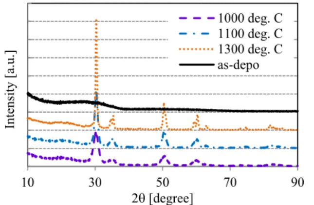
However, crystallization of Zr is expected by exposing to the high temperature, and propagation loss will be increased by this effect. To clarify the effect of crystallization, An X- ray diffraction (XRD) spectrum of the ZrO2-SiO2glass was measured. Figure 3 shows the measured XRD spectra. From this result, crystallized material was deposited when the an- nealing temperature became high. The deposited grain was found to be ZrO2by spectrum identification. The mean size of the grain was calculated by Scherrer equation written as
10 30 50 70 90
Intensity [a.u.]
2θ[degree]
1000 deg. C 1100 deg. C 1300 deg. C as-depo
Fig. 3 X-ray diffraction spectrum of ZrO2-SiO2glass related to anneal- ing temperature.
(a) Conventional process (b) Optimized process Core Side wall
Fig. 4 Picture of the core of ZrO2-SiO2PLC formed by dry etching.
equation (2):
τ= Kλ
βcosθ (2)
Whereτis the mean value of the grain size, K is a dimen- sionless shape factor,λis the X-ray wavelength,βis the line broadening at half the maximum intensity (FWHM),θis the Bragg angle. Calculated grain sizes at the annealing tem- perature of 1000, 1100, 1300 degree Celsius were 1.2, 2.0, 4.4 nm, respectively. The Grain size became larger as the annealing temperature became high. However, these grain sizes were far smaller than wavelength of the light used for optical communication.
3.2 Dry etching
Surface roughness of the core will cause scattering of the light and an increase of propagation loss. Figure 4 shows pictures of the core of the ZrO2-SiO2PLC after dry etching process. In the fabrication process of the PLC, waveguide patterns are formed by photolithography and dry etching af- ter glass deposition of an under clad and a core. As com- pared with GeO2which is used as a dopant of the conven- tional PLC, ZrO2has high steam pressure of reaction prod- ucts generated in the plasma etching process using halogen system gas as reactive gas [10]. Furthermore, for strong Zr- O coupling [10], ZrO2 is etching material with difficulty.
For these reasons, roughness of the sidewall of the ZrO2
doped core was generated during the dry etching process with the same process conditions as the conventional PLC.
Figure 4 (a) shows the core of the ZrO2-SiO2 PLC formed by dry etching with conventional process. The fabrication
Fig. 5 Spiral circuit for propagation loss measurement.
-2 0 2 4 6 8 10
0 10 20 30
Normalized insertion loss of test circuit [dB]
Length of the test circuit [cm]
Optimized process Conventional process
Fig. 6 Normalized insertion loss of the test circuit with various circuit length. Rate of increase of the insertion loss to circuit length is calculated as propagation loss.
process of the ZrO2-SiO2PLC was optimized to reduce the roughness of the sidewall of the core. Figure 4 (b) shows the core of the ZrO2-SiO2 PLC formed by optimized pro- cess. From this result, roughness of the sidewall was re- duced drastically, and scattering of the light was expected to be suppressed.
3.3 Propagation loss measurement
The propagation loss of the fabricated ZrO2-SiO2PLC was measured. A spiral circuit shown in Fig. 5 was used for the measurement. Insertion loss of the spiral circuit with differ- ent circuit length was measured, and the rate of increase of the insertion loss to circuit length was calculated as a prop- agation loss of the PLC. Fig 6 shows the calculated prop- agation loss of the ZrO2-SiO2 PLC. First, ZrO2-SiO2 glass of 5.5%-∆was deposited on the under clad, and annealing treatment was performed at the temperature of over 1000 de- gree Celsius. The size of the circuits using 5.5%-∆core was set to 3×3µm. When the spiral circuits were formed by the same process as the conventional PLC, measured propaga- tion loss was 0.2 dB/cm. The propagation loss of the ZrO2- SiO2 PLC is about one-tenth of that of the InP waveguide [4], and low propagation loss was achieved among waveg- uides consisting of high ∆material by the effective glass deposition and the annealing process. However, the prop- agation loss was still higher than that of the conventional PLC. Then, the propagation loss of the circuit formed by the optimized fabrication process was measured. As a re- sult, the propagation loss was successfully decreased to 0.02 dB/cm. Influence of the roughness of the sidewall of the core was clarified, and effect of the optimized fabrication
-0.1 0 0.1 0.2 0.3 0.4 0.5 0.6
0 200 400 600 800 1000
90-degree bending loss [dB]
Bending radius [µm]
Simulation Measurement
Fig. 7 Bending loss of the test circuit with various bending radius.
PLC
Pol.
TE
Pol.
TE/TM
Dep. OPM
TLS
Fig. 8 Setup for PER measurement.
24 µm 8µm
MMI length
Fig. 9 Schematic diagram of fabricated MMI coupler.
process was confirmed. The low propagation loss compa- rable as the conventional PLC was successfully achieved in the 5.5%-∆ZrO2-SiO2PLC.
4. Basic Optical Characteristics of ZrO2-SiO2PLC The Low loss 5.5%-∆ZrO2-SiO2PLC was realized by de- sign and investigation of the dopant for high∆silica glass shown in the Section II and the optimized fabrication pro- cess shown in the Section III. Basic optical characteristics of the ZrO2-SiO2PLC required for various optical devices are evaluated.
4.1 Minimum bending radius
A rminof the fabricated ZrO2-SiO2PLC was measured. Test circuits which comprised straight waveguide and bending waveguide with different bending radii were used for the measurement. Figure 7 shows 90-degree bending loss with different bending radii. This result indicated that rminof the ZrO2-SiO2PLC was 300µm. This result shows that rminof the ZrO2-SiO2 PLC was one-fifth or less as compared with that of the conventional PLC, and reduction of the chip size of the ZrO2-SiO2PLC was expected. This result agrees well with the result of the simulation shown as the solid line in
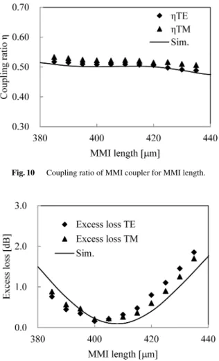
Fig. 10 Coupling ratio of MMI coupler for MMI length.
Fig. 11 Excess loss of MMI coupler for MMI length.
Fig. 7. From these results, we confirmed that the ZrO2-SiO2 PLC was fabricated properly as designed.
4.2 Polarization extinction ratio
Polarization extinction ratio (PER) of the ZrO2-SiO2 PLC was measured. Figure 8 shows a setup for the PER mea- surement. A tunable laser source (TLS) was used for the light source, and wavelength was set to 1550 nm. After pass through a depolarizer (Dep.), the light was launched into the PLC sandwiched between two polarizers. Intensity of the output light from the PLC was observed by an optical power meter (OPM). The polarizer (Pol.) which allowed to transmit transverse-electric (TE) wave was set to the input side of the PLC, and TE and transverse-magnetic (TM) Pol.
were used for the output side. The PLC with the wavy cir- cuit same as the one used in the rminmeasurement was used for the measurement. In the PLC, the TE Pol. launched a TE polarized light into the test circuit. If the light remains TE polarized, the light is shut offby the TM polarizer placed on the output side of the circuit, and then the high PER will be observed. The measured PER was 29 dB, and fine polar- ization maintaining characteristics was confirmed.
4.3 MMI coupler
In order to evaluate basic performance of the ZrO2-SiO2 PLC, we designed and fabricated a MMI coupler. The schematic diagram of the designed MMI coupler was shown in Fig. 9. Pitch of input and output waveguide and width of the MMI were set to 8µm and 24µm, respectively. Fig- ure 10 shows relationships between MMI length and cou- pling ratio of the fabricated MMI coupler, and excess loss for the MMI length was shown in Fig. 11. In Fig. 10 and Fig. 11, plots show measured values for the input light with TE and TM polarization, and solid lines show calculated values. The measured values agreed well with the simu- lation. Low excess loss of 0.2 dB and coupling ratio of 0.5 were achieved as designed. Coupling loss between the fab- ricated ZrO2-SiO2 PLC and SMF was about 2.7 dB/facet with simple horizontal taper. Reduction of the coupling loss is expected by optimized interface such as a spot-size con- verter.
5. Conclusion
For the downsizing of the chip and high density integra- tion required for the next generation PLC devices, compact silica-based PLC has been realized. The silica glass based 5.5%-∆PLC is realized by employing ZrO2which has high refractive index and low thermal expansion coefficient as a dopant. The chip size of the fabricated 5.5%-∆ZrO2-SiO2 PLC is reduced drastically to one twenty-fifth as compared with the conventional PLC due to its rminof 300µm.
The fabricated 5.5%-∆ZrO2-SiO2PLC has low propa- gation loss of 0.02 dB/cm, and PER of 29 dB. Fine charac- teristics of the MMI coupler are confirmed.
From these results, we confirmed that he ZrO2-SiO2
PLC is one of the most promising candidates for the next generation PLC devices.
References
[1] Y. Nasu, K. Watanabe, M. Itoh, H. Yamazaki, S. Kamei, R. Kasa- hara, I. Ogawa, A. Kaneko, and Y. Inoue, “Ultrasmall 100 GHz 40-channel VMUX/DEMUX based on single-chip 2.5%-∆PLC,” J.
Lightw. Technol., vol. 27, no. 12, pp. 2087–2094, June 2009.
[2] T. Inoue, H. Kawashima, and K. Nara, “Ultrasmall PBS-integrated coherent mixer using 1.8%-delta silica-based planar lightwave cir- cuit,” in Proc. ECOC2010, paper Mo.2.F.4, Sept. 2010.
[3] G. Bourdon, G. Alibert, A. Beguin, B. Bellman, and E. Guiot, “Ul- tralow loss ring resonators using 3.5% index-contrast Ge-doped sil- ica waveguides,” Photon. Technol. Lett., vol. 15, no. 5, pp. 709–711, May 2003.
[4] H. Yagi, N. Inoue, Y. Onishi, R. Masuyama, T. Katsuyama, T.
Kikuchi, Y. Yoneda, and H. Shoji, “High-efficient InP-based bal- anced photodiodes integrated with 90◦ hybrid MMI for compact 100 Gb/s coherent receiver,” in Proc. OFC2013, paper OW3J.5, Mar.
2013.
[5] U. Fischer, T. Zinke, J. R. Kropp, F. Arndt, and K. Petermann, “0.1 dB/cm waveguide losses in single-mode SOI rib waveguides,” Pho- ton. Technol. Lett., vol. 8, no. 5, pp. 647–648, May 1996.
[6] J.-J. He, B. Lamontagne, A. Delage, L. Erickson, M. Davies, and
E. S. Koteles, “Monolithic integrated wavelength demultiplexer based on a waveguide Rowland circle grating in InGaAsP/lnP,” J.
Lightw. Technol., vol. 16, no. 4, pp. 631–638, Apr. 1998.
[7] S. M. Edlou, A. Smajkiewicz, and G. A. Al-Jumaily, “Optical prop- erties and environmental stability of oxide coatings deposited by re- active sputtering,” Appl. Opt., vol. 32, no. 28, pp. 5601–5605, Oct.
1993.
[8] F. Lai, M. Li, K. Chen, H. Wang, Y. Song, and Y. Jiang, “Substrate temperature effect on the refractive index and a two-step film method to detect small inhomogeneities in optical films,” Appl. Opt., vol. 44, no. 29, pp. 6181–6185, Oct. 2005.
[9] “Zirconium and Hafnium” Mineral Commodity Summaries (US Ge- ological Survey), pp. 192–193. Jan. 2008.
[10] D. R. Lide, CRC Handbook of Chemistry and Physics 79th Edition, CRC Press, 1998.
Masanori Takahashi received the B.S. de- gree in electrical engineering from Waseda Uni- versity, Tokyo, Japan, in 2001. In 2001, he joined Furukawa Electric Co., Ltd., Ichihara, Chiba, where he has been engaged in research and development of silica-based planar light- wave circuits (PLCs) for optical communica- tions systems.
Yasuyoshi Uchida received the B.E. and M.S. degrees from Tokyo Institute of Technol- ogy, Tokyo, Japan, in 2004 and 2006, respec- tively. In 2006, he joined Furukawa Electric Co., Ltd., Ichihara, Chiba, where he has been engaged in research and development of planar lightwave circuit technologies and devices. Mr.
Uchida is a member of the Institute of Elec- tronics, Information and Communication Engi- neers of Japan and the Japan Society of Applied Physics.
Shintaro Yamasaki received the B.E. and M.S. degrees from Sophia University, Tokyo, Japan, in 2009 and 2011, respectively. In 2011, he joined Furukawa Electric Co., Ltd., Ichihara, Chiba, where he has been engaged in research and development of the process of Si-based pla- nar lightwave circuits (PLCs).
Junichi Hasegawa received the B.E. de- grees in Engineering from Utsunomiya Univer- sity and M.S. degrees in Engineering from To- hoku University in 1998, and 2000, respectively.
In 2000, he joined Furukawa Electric Co., Ltd., Ichihara, Chiba, where he has been engaged in research and development of optical communi- cation systems and devices.
Mr. Hasegawa is a member of the Institute of Electronics, Information and Communication Engineers.
Takeshi Yagi received the B. E., M. S. and Dr. Eng. degrees all from Tokyo Institute of Technology, Tokyo, Japan, in 1985, 1987 and 1990, respectively. In 1990, he joined The Fu- rukawa Electric Co., Ltd., where he has been engaged in research and development of opti- cal fibers. He is now a general manager of FI- TEL Photonics laboratory. Dr. Yagi is a member of the Institute of Electronics, Information and Communication Engineers.