Japan Advanced Institute of Science and Technology
JAIST Repository
https://dspace.jaist.ac.jp/Title
First principles study of the electronic and optical properties of crystalline and liquid Sb_2Te_3: Phase-transition-induced changes in optical properties
Author(s) Sano, Haruyuki; Kuwahara, Masashi; Mizutani, Goro Citation Japanese Journal of Applied Physics, 57(9S1):
09SD01-1-09SD01-6 Issue Date 2018-07-27
Type Journal Article
Text version author
URL http://hdl.handle.net/10119/16075
Rights
This is the author's version of the work. It is posted here by permission of The Japan Society of Applied Physics. Copyright (C) 2018 The Japan Society of Applied Physics. Haruyuki Sano, Masashi Kuwahara, and Goro Mizutani, Japanese Journal of Applied Physics, 57(9S1), 2018, 09SD01-1-09SD01-6.
http://dx.doi.org/10.7567/JJAP.57.09SD01 Description
1
First principles study of the electronic and optical properties of
crystalline and liquid Sb
2Te
3: phase-transition-induced changes in
optical properties
Haruyuki Sano1*, Masashi Kuwahara2, and Goro Mizutani3
1 National Institute of Technology, Ishikawa College, Tsubata, Ishikawa 929-0392
Japan
2 Electronics and Photonics Research Institute, National Institute of Advanced
Industrial Science and Technology, Tsukuba, Ibaraki 305-8565 Japan
3 School of Materials Science, Japan Advanced Institute of Science and Technology,
Nomi, Ishikawa 923-1292 Japan
*E-mail: [email protected]
To clarify the mechanism by which the optical properties of Sb2Te3 change because of its
solid–liquid phase transition, we carried out ab initio calculations of the electronic and optical properties of Sb2Te3 in both the crystalline and liquid states. The calculated results
indicate that the density of states around the Fermi level increases because of melting and that the energy bandgap observed in the crystalline state consequently disappears. The imaginary part of optical dielectric functions of crystalline Sb2Te3 has a large peak at a
photon energy of ω = 1.5 eV. When Sb2Te3 melts, it exhibits somewhat metallic optical
properties and its optical absorption at ω = 3.06 eV, which is used in Blu-ray Disc systems, decreases. This decrease in optical absorption is proposed to result from a large reduction of the optical transition strength at ω ≈ 1.5 eV.
2
1. Introduction
Super-resolution readout (SRR) technology1-8) is one of the most promising technologies to
realize high-density optical disks. An active layer with optical nonlinearity is the key to this technology. The heat produced by laser-light irradiation causes melting within a small region of an active layer. The small molten region, whose optical properties change because of the phase transition, behaves like a small aperture9) or small mask10-12) for the
light exposure. This effect is essential for the super-resolution mechanism. Therefore, fully understanding the mechanism of the melting-induced change in optical properties of the active-layer material is necessary for the development of SRR technology.
Antimonides such as Sb2Te3 and InSb are the best candidate materials for the active
layer in a super-resolution optical disk.8, 13) These two materials, which are
narrow-bandgap semiconductors in their crystalline state, exhibit phase-transition-induced changes in their optical properties. Specifically, the optical absorption of Sb2Te3 at a
photon energy ( ω) of 3.06 eV, which is used in Blu-ray Disc systems, decreases because of the melting, whereas that of InSb increases. Kuwahara et al. experimentally investigated the details of the changes in the optical properties of Sb2Te314, 15) and InSb.16) Their
spectroscopic ellipsometry measurements showed that the optical dielectric functions in the solid state included several peaks corresponding to interband transitions and that, after the samples melted, the functions became Drude-like. The experimental data do not provide sufficient information about the mechanism of the changes in the optical properties of Sb2Te3 and InSb due to melting. Thus, clarifying this mechanism and understanding the
origin of the difference in the optical-absorption changes between Sb2Te3 and InSb require
a comprehensive analysis using ab initio calculations of their electronic and optical properties.
We have already reported ab initio calculations of the electronic and optical properties of InSb for both the crystalline and liquid states,17) and we proposed that the
melting-induced increase in the optical absorption at ω = 3.06 eV originates from the increased optical transitions below 2 eV. The literature18-25) contains numerous ab initio
studies on the electronic states of Sb2Te3 in its crystalline state because this material has
recently attracted attention as a topological insulator. Several calculations of the optical properties of crystalline and amorphous Sb2Te3 have also been reported.26-31) However, ab
initio calculations of the optical properties of liquid Sb2Te3 have not yet been reported.
Therefore, in the present study, we have carried out ab initio calculations of the electronic states and optical dielectric functions of both crystalline and liquid Sb2Te3. Because the
3
same calculation code and similar approximation parameters were used for a series of our theoretical studies, the calculated results can be used to quantitatively compare the two phases and, in particular, to investigate the difference between Sb2Te3 and InSb. These
quantitative comparisons are important for clarifying the general mechanism of the melting-induced changes in optical properties.
Some of the results of our current calculation—specifically, the total electronic density of states (DOS) and the imaginary part of the refractive indices—have been reported elsewhere.32) In the present paper, we present new data related to our calculation
results for the electronic band structures, partial DOS, optical dielectric functions, and complex refractive indices, which are substantiated by a more detailed analysis and discussion.
2. Methods
This study was performed using the projector augmented-wave method33, 34) including
spin–orbit coupling (SOC) effects, as implemented in the Vienna Ab initio Simulation Package (VASP).35, 36) When the generalized gradient approximation (GGA) or the
local-density approximation (LDA) is used in standard density functional theory, the band-gap energy of semiconductors is underestimated. In particular, no gap is observed in band structures calculated for narrow-band-gap semiconductors such as InSb. To overcome this problem without additional large computational cost, the modified Becke–Johnson exchange potential combined with the local-density approximation (MBJLDA) method37)
was used in the present study. As already reported, the MBJLDA method provides accurate gap-energy values for InSb.17, 38) The Brillouin-zone (BZ) integration was performed on
-centered k-point meshes using the Gaussian smearing method with a width of 0.1 eV. For the crystalline and liquid states of Sb2Te3, (20 × 20 × 20) and (3 × 3 × 3) k points were
used, respectively. Optical dielectric functions () were obtained by calculating the electronic transitions within the electric dipole approximation.39) Intraband transitions
expressed by the Drude-like term in the dielectric function were not considered in this calculation. The complex refractive indices ( ) were obtained using the relation
√ .
For the calculation of crystalline Sb2Te3, a rhombohedral unit-cell structure with space
group ( 3 ) was used. As shown in Fig. 1(a), the unit cell has three inequivalent atoms: Sb, Te1, and Te2. The experimentally measured lattice parameters,40) i.e., a = 0.425
4
nm, c = 3.04 nm, Sb position u = 0.400, and Te position v = 0.211, were adopted in the calculation for the crystalline state. Model atomic structures for liquid Sb2Te3 at a
temperature of 1200 K were constructed using ab initio molecular dynamics (MD) simulations17) as follows. A cubic supercell with a lattice parameter of 2.044 nm included
94 Sb atoms and 141 Te atoms. This model size was determined according to the previous MD simulations for liquid and amorphous Sb2Te3, reported by Caravati et al.13) Their
calculations enabled the employment of their results to be used for sufficient discussions on liquid and amorphous structures. We also confirmed that this size was sufficient for the optical properties, by performing calculations on models with different sizes. The density of the liquid model at 1200 K was set to be 5.72 × 10³ kg/m3, which was estimated from
experimental data of the density of liquid Sb2Te3.41) The MD calculations were performed
within the GGA with no consideration of SOC effects and using only the -point in the BZ integration. A canonical ensemble with a Nosé thermostat42) was used for temperature
control, and the time step was set to be 3 fs. The temperature was changed as shown in Fig. 2(a). After reaching thermodynamic equilibrium at 1200 K, we obtained two model atomic structures for liquid Sb2Te3 as snapshots at two different time points (LA and LB). For
these two model structures, which are shown in Fig. 2(b) and 2(c), the electronic states and optical properties were calculated. The calculated results (DOS and ) for these two model structures were very similar and only had small differences. Therefore, they displayed no prominent features resulting from structural peculiarities. An averaging operation for the two sets of calculated results was performed to eliminate the remaining effects of small structural peculiarities.17)
In this study, the optical properties of crystalline Sb2Te3 were measured for
comparison with the calculated results. The sample was a polished bulk crystal. A spectroscopic ellipsometer (J. A. Woollam, M-2000) was used to obtain refractive-index spectra in the wavelength range from 300 to 1000 nm.
3. Results and discussion
The calculated electronic energy band structures of crystalline Sb2Te3 are shown in Fig. 3.
The symbols U, a, , Z, F, and L denote high-symmetry k points defined in the BZ of Fig. 1(b). The band opening observed along the high-symmetry line indicates that crystalline Sb2Te3 has a semiconductor-like electronic structure. The band topology near the Fermi
5
31) Figure 4 shows the DOS of crystalline Sb
2Te3 calculated using a Gaussian smearing of
0.1 eV. The band-gap energy was estimated to be 0.15 eV from the DOS calculation using a very small smearing (0.001 eV). The optical gap, which represents an absorption edge, was also calculated to be 0.20 eV. These values are consistent with the experimental value of 0.21 eV determined as indirect transitions43) and the previously reported values 0.15–
0.22 eV.44) The partial DOSs in Fig. 4(b)–(d) suggest that the bands in crystalline Sb 2Te3
originate as follows. Relatively narrow bands around the energies −11.5 eV and −9.5 eV are attributed to the s-orbitals of Te and Sb, respectively. A band just below the Fermi level, i.e., in the range from −2 to 0 eV, is attributed to the mixing of the p-orbital of Te and the
s-orbital of Sb.
The DOS of liquid Sb2Te3 is shown in Fig. 5. The total DOS in Fig. 5(a) agrees well
with that reported by Caravati et al.13) The partial DOSs in Fig. 5(b) and 5(c) are the
average of 141 Te atoms and 94 Sb atoms, respectively. The phase transition from the crystalline to the liquid state causes a drastic change in the DOS compared with that in Fig. 4. Specifically, the DOS near the Fermi level increases and the energy gap disappears. A similar change is observed for InSb.17) Thus, from the viewpoint of the DOS, the melting
appears to induce metallic electronic states in both Sb2Te3 and InSb.
The mechanism of melting-induced metallization of the electronic states of covalent semiconductors is explained as follows. Consider the example of InSb, in which atoms in the crystalline phase are four-coordinate and the valence band, which is formed from the bonding state between In and Sb atoms below the Fermi level, is completely filled with electrons. Actually, ab initio calculations45) indicate that valence electrons are localized
between the In and Sb atoms to form the bonding state. However, the conduction band formed from the antibonding state is empty. When InSb melts and its structural order is lost, the variations in nearest-neighbor distances and coordination numbers increase. According to Gu et al.,46) both the average nearest-neighbor distance and the average coordination
number become greater than those in the crystalline phase and the compositional disorder number is 0.66, meaning that a substantial number of homogeneous bonds (In–In and Sb– Sb) exist in the liquid phase. Because of these geometrical changes, various electronic states with less bonding character than in crystalline InSb are formed around the Fermi level and electrons in these states are more delocalized than in the crystal. Consequently, the molten InSb exhibits metallic properties.
Figures 6 and 7 show the optical dielectric functions and refractive indices of Sb2Te3
6
calculated results for crystalline and liquid Sb2Te3, respectively. The thick solid line and
thick dashed line are the experimental data for the polished crystalline Sb2Te3 and liquid
Sb2Te3,14) respectively. Because a Sb2Te3 crystal has anisotropy, the optical response differs
in the parallel (z) and perpendicular (x and y) directions relative to the c-axis. Here, the calculated results (thin solid lines) in Figs. 6 and 7 are averaged over the x, y, and z directions. In the optical calculations, the Fermi–Dirac function at zero temperature was used as the electron occupancy distribution. Note that even when using the Fermi–Dirac function at 1200 K, the calculated results of liquid Sb2Te3 did not change in the energy
range above 0.5 eV.
The calculated imaginary part of the dielectric function (Im[ε]) of crystalline Sb2Te3
includes a large peak at ω = 1.5 eV, as shown by the thin solid line in Fig. 6(a). This calculated result well reproduces the experimental data with a peak at ω = 1.63 eV (thick solid line). Our calculated complex dielectric functions are also consistent with other theoretical studies26, 27, 31) from the viewpoint of shape, peak position, and absolute value.
The Im[ε] represents the strength of the optical transitions from occupied states to empty states. Therefore, the partial DOSs in Fig. 4(b)–(d) suggest that the peak at ω = 1.5 eV originates in the optical transitions from the s-band of Sb at approximately −0.9 eV to the
p-band of Sb or Te2 at approximately 1 eV.
As shown in Figs. 6 and 7, with the phase transition of the Sb2Te3 to liquid, its optical
responses change greatly. The calculated results for liquid Sb2Te3 (dotted line)
approximately reproduce the experimental features (thick dashed line) in that both the real (Re[ε]) and imaginary (Im[ε]) parts of the dielectric function increase as ω decreases. As previously described, liquid Sb2Te3 shows a typical metallic DOS. Generally, a metal has a
large negative value of Re[ε] in the visible-light region, e.g., Re[ε] = −15 at ω = 2 eV for silver,47) and as ω decreases, the Re[ε] of the metal decreases divergently, whereas the
Im[ε] of the metal increases divergently. The calculated Im[ε] of liquid Sb2Te3 (dotted line
in Fig. 6(a)) shows such typical metallic behavior. However, the calculated Re[ε] of liquid Sb2Te3 (dotted line in Fig. 6(b)) has a small negative value in the visible-light region, e.g.,
−1.2 at ω = 2 eV, and the experimental Re[ε] values (thick dashed line) are even positive. These results indicate that the optical properties of liquid Sb2Te3 differ from those typically
observed for a metal. According to the electrical resistivity48) and NMR49) measurements,
the electrical resistivity of liquid Sb2Te3 has a value near the boundary between the value
for a metal and the value for a semiconductor and exhibits a negative temperature dependence, typical of a semiconductor; however, the conduction electrons of liquid
7
Sb2Te3 also exhibit metallic character in that they are not localized on a particular atomic
site. Thus, these unique electronic states of liquid Sb2Te3 are considered as the origin of the
optical response in which both metallic and nonmetallic properties are mixed.
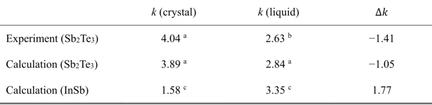
Next, we consider the optical absorption at a photon energy of ω = 3.06 eV, which is important for active-layer materials in super-resolution optical disks. The values of the imaginary part of the refractive index (k) representing the optical absorption are shown in Table I. The experimental values of k for Sb2Te3 clearly decrease because of the melting,
and this result is roughly reproduced by the calculation. We shall discuss the mechanism of the decrease in k due to the melting. As shown in Fig. 6(a), the value of Im[ε] of liquid Sb2Te3 at ω = 3.06 eV (dotted line) is quite similar to that of crystalline Sb2Te3 (thin solid
line); that is, the strength of the optical transitions at ω = 3.06 eV does not change as a result of the melting. Therefore, the optical transitions at ω = 3.06 eV do not affect the decrease in k. In the case where Im[ε] does not change, the decrease in k should result from the change in Re[ε] from a large negative value to a small negative or positive value, as derived from the following equation with the complex square root: √ . Actually, as shown in Fig. 6(b), Re[ε] at ω = 3.06 eV greatly increases from −13 to −4.5 (+5.2 for the experiment) because of the melting. According to the Drude–Lorentz model, the increase in Re[ε] at ω = 3.06 eV should be caused by a reduction of the optical transitions below 3.06 eV, which is actually observed as the disappearance of the large peak of Im[ε] at ω = 1.5 eV because of the melting. In conclusion, the results suggest that the large optical transition peak of crystalline Sb2Te3 at ω ≈ 1.5 eV disappear because of
the melting, and this reduction of the optical transitions at ω ≈ 1.5 eV causes the decrease in optical absorption at ω = 3.06 eV.
Finally, we discuss the difference in the changes in the optical properties between Sb2Te3 and InSb. For this comparison, the calculated results for k and Im[ε] for both Sb2Te3
(this work) and InSb17) are shown in Fig. 8, and the value of k at ω = 3.06 eV for InSb17)
is also shown in Table I. As indicated by the upward arrow in Fig. 8(a), k or the optical absorption at ω = 3.06 eV for InSb increases because of the melting. This change is opposite to that encountered for Sb2Te3. We reported the detailed mechanism of the change
in optical absorption of InSb in a previous paper.17) Briefly, the optical transition strength
of InSb at ω < 2 eV, which is very small in the crystalline state, greatly increases when the electronic state of InSb is metallized because of the melting (as indicated by the upward arrow in Fig. 8(b)). This change in the optical transition strength causes an increase
8
of the optical absorption at ω = 3.06 eV. As shown in Fig. 8, liquid Sb2Te3 (dotted line)
and liquid InSb (thick dashed line) have similar values for both k and Im[ε] over a wide photon energy range. Thus, the difference in the optical absorption change at ω = 3.06 eV between Sb2Te3 and InSb must result from the difference in electronic states between the
two materials in their crystalline state. In Fig. 8(b), although the values of Im[ε] at ω = 3.06 eV are the same for Sb2Te3 and InSb, a large difference is observed at ω < 2 eV.
Specifically, the Im[ε] of crystalline Sb2Te3 is very large and the Im[ε] of crystalline InSb is
very small. This difference in Im[ε] at ω < 2 eV represents the difference in electronic states near the Fermi level between crystalline Sb2Te3 and InSb. As indicated by the DOSs
in the inset of Fig. 8(b), the energy separation between the valence band and the conduction band is small (~1.5 eV) for crystalline Sb2Te3, which contributes to the large
optical transition peak at approximately 1.5 eV. However, the energy separation for crystalline InSb is relatively large (~4 eV); thus, the Im[ε] associated with optical transitions and having an energy distance of less than 2 eV is observed to be small. In conclusion, we propose that the difference in the electronic states near the Fermi level between crystalline Sb2Te3 and InSb results in the difference in the melting-induced optical
absorption change at 3.06 eV.
4. Conclusions
We performed ab initio calculations of the electronic and optical properties for both crystalline and liquid Sb2Te3. The calculated DOSs show that the energy bandgap in the
crystalline state disappears because of the melting and that the optical properties of Sb2Te3
become somewhat metallic. We propose that the melting-induced decrease in optical absorption at ω = 3.06 eV is caused by the decreased optical transitions at ω = 1.5 eV and that the difference in the melting-induced change in the optical properties between Sb2Te3 and InSb results from the difference in their electronic states near the Fermi level in
their crystalline states.
Acknowledgment
9
References
1) M. Kaneko, K. Aratani, and M. Ohta, Jpn. J. Appl. Phys. 31, 568 (1992).
2) K. Yasuda, M. Ono, K. Aratani, A. Fukumoto, and M. Kaneko, Jpn. J. Appl. Phys. 32, 5210 (1993).
3) J. Tominaga, T. Nakano, and N. Atoda, Appl. Phys. Lett. 73, 2078 (1998).
4) T. Kikukawa, N. Fukuzawa, and T. Kobayashi, Jpn. J. Appl. Phys. 44, 3596 (2005). 5) J. Kim, I. Hwang, J. Bae, J. Lee, H. Park, I. Park, T. Kikukawa, N. Fukuzawa, T. Kobayashi,
and J. Tominaga, Jpn. J. Appl. Phys. 45, 1370 (2006).
6) M. Kuwahara, T. Shima, P. Fons, T. Fukaya, and J. Tominaga, J. Appl. Phys. 100, 043106 (2006).
7) K. Nakai, M. Ohmaki, N. Takeshita, B. Hyot, B. André, and L. Poupinet, Jpn. J. Appl. Phys. 49, 08KE01 (2010).
8) B. Hyot, Phys. Status Solidi B 249, 1992 (2012).
9) J. S. Kim, K. Kwak, and C. Y. You, Jpn. J. Appl. Phys. 47, 5845 (2008).
10) A. C. Assafrao, A. J. H. Wachters, S. F. Pereira, and H. P. Urbach, Jpn. J. Appl. Phys. 51, 112501 (2012).
11) H. Sano, T. Shima, M. Kuwahara, Y. Fujita, M. Uchiyama, and Y. Aono, J. Appl. Phys. 115, 153104 (2014).
12) H. Sano, T. Shima, M. Kuwahara, Y. Fujita, M. Uchiyama, and Y. Aono, Jpn. J. Appl. Phys. 55, 09SB02 (2016).
13) S. Caravati, M. Bernasconi, and M. Parrinello, Phys. Rev. B 81, 014201 (2010).
14) M. Kuwahara, R. Endo, K. Tsutsumi, F. Morikasa, T. Tsuruoka, T. Fukaya, M. Suzuki, M. Susa, T. Endo, and T. Tadokoro, Appl. Phys. Lett. 100, 101910 (1012).
15) M. Kuwahara, R. Endo, K. Tsutsumi, F. Morikasa, T. Tsuruoka, T. Fukaya, M. Suzuki, M. Susa, T. Endo, and T. Tadokoro, Jpn. J. Appl. Phys. 52, 118001 (1013).
16) M. Kuwahara, R. Endo, K. Tsutsumi, F. Morikasa, M. Suzuki, T. Shima, M. Susa, T. Endo, T. Tadokoro, and S. Hosaka, Appl. Phys. Express 6, 082501 (2013).
17) H. Sano and G. Mizutani, AIP Adv. 5, 117110 (2015).
18) T. Thonhauser, T. J. Scheidemantel, J. O. Sofo, J. V. Badding, and G. D. Mahan, Phys. Rev. B 68, 085201 (2003).
19) P. Larson, Phys. Rev. B 74, 205113 (2006).
20) G. Wang and T. Cagin, Phys. Rev. B 76, 075201 (2007).
21) M. S. Park, J. H. Song, J. E. Medvedeva, M. Kim, I. G. Kim, and A. J. Freeman, Phys. Rev. B 81, 155211 (2010).
22) L. Xuelai, S. Zhimei, S. Zhitang, R. Feng, W. Liangcai, and L. Weili, Solid State Sci. 13, 131 (2011).
23) J. M. Zhang, W. Ming, Z. Huang, G. B. Liu, X. Kou, Y. Fan, K. L. Wang, and Y. Yao, Phys. Rev B 88, 235131 (2013).
24) K. Zhao, Y. Wang, Y. Sui, C. Xin, X. Wang, Y. Wang, Z. Liu, and B. Li, Phys. Status Solidi RRL 9, 379 (2015).
25) K. H. Jin, H. W. Yeom, and S. H. Jhi, Phys. Rev. B 93, 075308 (2016).
26) J. W. Park, S. H. Eom, H. Lee, J. L. F. Da Silva, Y. S. Kang, T. Y. Lee, and Y. H. Khang, Phys. Rev. B 80, 115209 (2009).
27) S. Caravati, M. Mernasconi, and M. Parrinello, J. Phys.: Condens. Matter 22, 315801 (2010).
28) S. Liu, J. Wei, and F. Gan, Appl. Phys. Lett. 100, 111903 (2012). 29) H. Koc, A. M. Mamedov, and E. Ozbay, Ferroelectrics 448, 29 (2013).
30) J. J. Carey, J. P. Allen, D. O. Scanlon, and G. W. Watson, J. Solid State Chem. 213, 116 (2014).
31) I. A. Nechaev, I. Aguilera, V. De Renzi, A. di Bona, A. Lodi Rizzini, A. M. Mio, G. Nicotra, A. Politano, S. Scalese, Z. S. Aliev, M. B. Babanly, C. Friedrich, S. Blügel, and E. V. Chulkov, Phys. Rev. B 91, 245123 (2015).
32) H. Sano, M. Kuwahara, and G. Mizutani, Tech. Dig. Int. Symp. Imaging, Sensing, Optical Memory, 2017, pp. 55-56.
33) G. Kresse and D. Joubert, Phys. Rev. B 59, 1758 (1999). 34) P. E. Blöchl, Phys. Rev. B 50, 17953 (1994).
10
36) G. Kresse and J. Furthmüller, Phys. Rev. B 54, 11169 (1996). 37) F. Tran and P. Blaha, Phys. Rev. Lett. 102, 226401 (2009).
38) Y-S. Kim, M. Marsman, G. Kresse, F. Tran, and P. Blaha, Phys. Rev. B 82, 205212 (2010). 39) M. Gajdoš, K. Hummer, G. Kresse, J. Furthmüller, and F. Bechstedt, Phys. Rev. B 73,
045112 (2006).
40) R. W. G. Wyckoff, Crystal Structures (Wiley, New York, 1964), Vol. 2, p. 30. 41) K. J. Singh, R Satoh, and Y. Tsuchiya, J. Phys. Soc. Jpn. 72, 2546 (2003). 42) S. Nosé, J. Chem. Phys. 81, 511 (1984).
43) R. Sehr and L. R. Testardi, J. Phys. Chem. Solids 23, 1219 (1962).
44) J. K. Olson, H. Li, T. Ju, J. M. Viner, and P. C. Taylor, J. Appl. Phys. 99, 103508 (2006), and references therein.
45) J. R. Chelikowsky and M. L. Cohen, Phys. Rev. B 14, 556 (1976). 46) T. Gu, X. Bian, J. Qin, and C. Xu, Phys. Rev. B 71, 104206 (2005).
47) D. W. Lynch and W. R. Hunter, in Handbook of Optical Constants of Solids, ed. E. D. Palik (Academic Press, New York, 1985) pp. 350-357.
48) R. Endo, S. Maeda, Y. Jinnai, R. Lan, M. Kuwahara, Y. Kobayashi, and M Susa, Jpn. J. Appl. Phys. 49, 065802 (2010).
11
Figure captions
Fig. 1. (Color online) (a) Crystal structure and (b) Brillouin zone (BZ) of Sb2Te3.
Fig. 2. (Color online) (a) Temperature control of the MD calculation and (b) (c) model atomic structures of liquid Sb2Te3. The dashed horizontal line in panel (a) denotes the
melting point of Sb2Te3. (b) LA and (c) LB denote snapshots at different time points in the
MD calculation at 1200 K.
Fig. 3. (Color online) (a) Electronic energy band structures of crystalline Sb2Te3 in the
wide energy range from −15 eV to 15 eV. In panel (b), the vertical axis is magnified around the Fermi level. The symbols U, a, Γ, Z, F, and L denote high-symmetry k points defined in the BZ of Fig. 1(b).
Fig. 4. (Color online) Electronic density of states (DOS) of crystalline Sb2Te3: (a) total
DOS; partial DOS projected onto the molecular orbitals of (b) Te1, (c) Te2, and (d) Sb. Fig. 5. (Color online) Electronic density of states (DOS) of liquid Sb2Te3: (a) total DOS;
partial DOS projected onto the molecular orbitals of (b) Te and (c) Sb.
Fig. 6. (Color online) (a) Imaginary and (b) real parts of the optical dielectric functions. The thin solid line and dotted line show the calculated dielectric functions of crystalline and liquid Sb2Te3, respectively. The thick solid line and thick dashed line are experimental
data for the polished crystal Sb2Te3 and liquid Sb2Te3,14) respectively.
Fig. 7. (Color online) (a) Imaginary and (b) real parts of the refractive indices. The thin solid line and dotted line show the calculated refractive indices of crystalline and liquid Sb2Te3, respectively. The thick solid line and thick dashed line are experimental data for
polished crystalline Sb2Te3 and liquid Sb2Te3,14) respectively.
Fig. 8. (Color online) Imaginary parts of (a) the refractive indices and (b) dielectric functions. The thin solid line and dotted line show the calculated results (this work) for crystalline and liquid Sb2Te3, respectively. The thick solid line and thick dashed line show
the calculated results17) for crystalline and liquid InSb, respectively. The inset of (b) is the
12
Table I. Imaginary part of the refractive index (k) at a photon energy of ω = 3.06 eV.
k (crystal) k (liquid) ∆ Experiment (Sb2Te3) 4.04 a 2.63 b −1.41 Calculation (Sb2Te3) 3.89 a 2.84 a −1.05 Calculation (InSb) 1.58 c 3.35 c 1.77 a This study. b Ref. 14. c Ref. 17.
13 Fig. 1. (Color online)
14 Fig. 3. (Color online)
15 Fig. 4. (Color online)
16 Fig. 6. (Color online)
17 Fig. 8. (Color online)