https://dspace.jaist.ac.jp/
Title
Behavior of the potential-induced degradation of photovoltaic modules fabricated using flat mono-crystalline silicon cells with different surface orientations
Author(s) Yamaguchi, Seira; Masuda, Atsushi; Ohdaira, Keisuke
Citation Japanese Journal of Applied Physics, 55(4S): 04ES14-1-04ES14-5
Issue Date 2016-03-24
Type Journal Article
Text version author
URL http://hdl.handle.net/10119/16135
Rights
This is the author's version of the work. It is posted here by permission of The Japan Society of Applied Physics. Copyright (C) 2016 The Japan Society of Applied Physics. Seira Yamaguchi, Atsushi Masuda and Keisuke Ohdaira, Japanese Journal of Applied Physics, 55(4S), 2016, 04ES14. http://dx.doi.org/10.7567/JJAP.55.04ES14
Seira Yamaguchi , Atsushi Masuda , and Keisuke Ohdaira
1School of Materials Science, Japan Advanced Institute of Science and Technology (JAIST), Nomi, Ishikawa 923-1292, Japan
2Research Center for Photovoltaics, National Institute of Advanced Industrial Science and Technology (AIST), Tsukuba, Ibaraki 305-8568, Japan
3Green Device Research Center, Japan Advanced Institute of Science and Technology (JAIST), Nomi, Ishikawa 923-1292, Japan
This paper deals with the dependence of the potential-induced degradation (PID) of flat, p-type mono-crystalline silicon solar cell modules on the surface orientation of solar cells. The investigated modules were fabricated from p-type mono-crystalline silicon cells with a (100) or (111) surface orientation using a module laminator. PID tests were performed by applying a voltage of −1000 V to shorted module in-terconnector ribbons with respect to an Al plate placed on the cover glass of the modules at 85 ◦C. A decrease in the parallel resistance of the (100)-oriented cell modules is more significant than that of the (111)-oriented cell modules. Hence, the performance of the (100)-oriented-cell modules drastically deteri-orates, compared with that of the (111)-oriented-cell modules. This implies that (111)-oriented cells offer a higher PID resistance.
1. Introduction
The potential-induced degradation (PID) of Si-wafer-based photovoltaic (PV) modules has been identified as one of the most important reliability issues. Very large scale PV systems, which can generate a high electric power, have been installed worldwide over the last decade. PV modules in such systems can be exposed to high electrical potential differences from their grounded frames. These may trigger PID, which can cause significant performance losses in the modules.1–3)
The PID of p-type crystalline Si (c-Si) PV modules is characterized by a reduction in the shunt resistance Rp1) and the enhancement of depletion region recombination.4, 5) The PID
of p-type c-Si PV modules can be attributed to alkali metal ions, e.g., Na+, migrating from a
module cover glass owing to high voltages.3)Naumann et al.6)have revealed that Na
accumu-lates in the silicon nitride (SiNx)/Si interface of c-Si solar cells in PID-affected regions. It has
also been reported that both PID shunts and Na accumulation occur locally.7, 8)Moreover, they
have found that stacking faults existing in c-Si contaminated by Na play an important role in PID.9) Some research groups have proposed physical models that can explain the shunting based on Na-decorated intrinsic stacking faults.9–11)Recently, Ziebarth et al.12)have provided further detailed discussion about the diffusion of Na in intrinsic stacking faults and the short-circuiting of p–n junctions by theoretical calculations based on the density functional theory. Very recently, Wilson et al.13)have investigated in detail the drift characteristics of Na ions in
SiNx films where an electric field exists.
The PID of c-Si PV modules is influenced by module components, such as a cover glass, encapsulant, and cells. It has been demonstrated that no significant PID occurs in c-Si PV modules with a quartz cover glass,4) aluminosilicate chemically strengthened glass,14) or an acrylic thin film15) instead of conventional tempered glass. PID can be prevented by the use of a high-electric-resistance encapsulant,4, 16) by inserting a polyethylene17)or an ionomer18) thin film between an ethylene-vinyl acetate copolymer (EVA) encapsulant and a front cover glass or cells, or by increasing the cross-linkage level or the thickness of the encapsulant.19)
PID resistance is also affected by the refractive index2, 20, 21)or thickness2) of an SiN
x
antire-flective coating (ARC) layer on the emitter layer of a c-Si PV cell. PID can therefore be also suppressed by the composition control of the ARC layers. However, it is not very desirable to change the refractive index from conventional and optimized values because of the enhance-ment of parasitic absorption. Mishina et al.22, 23)have shown that a high PID resistance can be realized by using PV cells with ARC layers having a conventional refractive index prepared by plasma-enhanced chemical vapor deposition (PECVD) using a hollow cathode. Hara et
al.24) have reported that TiO2 thin films deposited on the inner surfaces of a cover glass can
prevent PID for c-Si modules. Du et al.25) have shown that the PID of c-Si solar cells can be
effectively reduced without influencing their efficiency by inserting phosphorus silicate glass (PSG) layers between the front n+emitters and the SiNx ARC layers. PID-affected modules
can recover from the degradation by applying a positive bias.2, 3) The recovery is explained
by a diffusion-driven process.9, 10, 26)
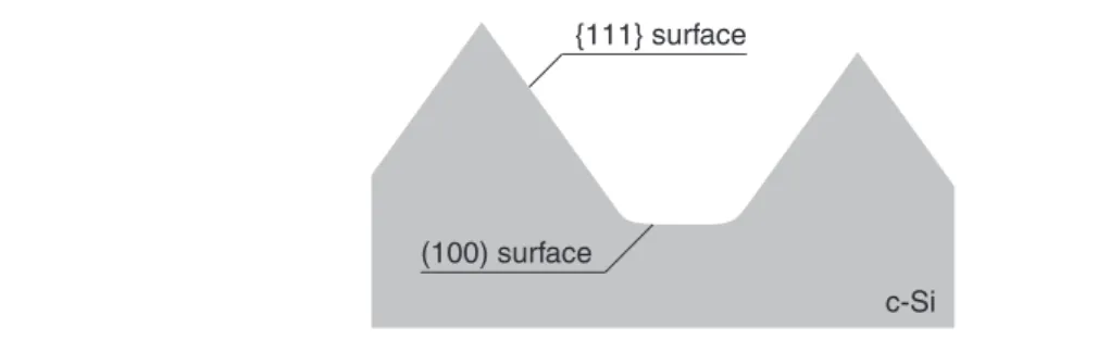
Recently, Chen et al.27) have reported that the shape of the textured surface of c-Si can influence its PID resistance. They have demonstrated that cells having groove-rounded tex-ture exhibit a higher PID resistance.27)Detailed discussion has, however, not been made thus far. Groove-rounded cells generally have partially residual (100)-oriented surfaces as well
Fig. 1. Schematic diagram of a rounded groove between micrometer-sized pyramids. The rounded groove is characterized by a residual (100) surface.
as{111}-oriented ones belonging to micrometer-sized pyramids, as illustrated in Fig. 1. The higher PID resistance of groove-rounded textured cells may be affected by the surface orien-tation of c-Si cells.
In the present work, we investigate the effect of the surface orientation of c-Si cells on PID resistance, by comparing the results of PID tests on modules fabricated using p-type flat (100)- and (111)-oriented cells. On the basis of the obtained results, we also discuss the higher PID resistance of groove-rounded textured cells demonstrated by Chen et al. Our findings may provide an improved explanation of the effect of the surface morphology of cells on PID resistance.
2. Experimental procedure
(100)- or (111)-oriented, one-side polished p-type c-Si wafers were cut to 20× 20 mm2-sized
substrates. The front surface of the substrates was coated with a liquid PSG source (Tokyo Ohka Kogyo, SC-913) by spin coating, and the substrates were subsequently annealed at 850
◦C for 25 min in N
2 atmosphere in order to form n+ emitters. The emitters on the flat c-Si
surfaces had a sheet resistance of∼30 Ω/sq. After the removal of the phosphorus silicate glass remaining on the c-Si surfaces, SiNx ARC films with a thickness of∼70 nm were deposited
onto the n+ emitter surfaces by catalytic CVD (Cat-CVD),28) which is also referred to as
hot-wire CVD. The thickness and refractive indices of the SiNx ARC films on the (100) and
(111) substrates were almost the same, and we considered that the films deposited on both substrates had the same properties. Ag paste was printed onto the front surfaces of the c-Si substrates by screen printing, followed by the screen printing of Al and Ag pastes on their rear sides. The samples were then fired at a peak temperature of 800◦C in air atmosphere in a tube furnace to form electrical contact. After the metalization, edge isolation was carried out by shaving the edges of the cells with sandpaper.29)
pre-Fig. 2. (Color online) Appearance of a fabricated module. The cell has a size of 20× 20 mm2, and the module has a size of 45× 45 mm2.
pared stacks composed of cover glass/EVA encapsulant/c-Si cell/EVA encapsulant/typical backsheet [poly(vinyl fluoride) (PVF)/poly(ethylene terephthalate) (PET)/PVF]. The cover glass has a size of 45× 45 mm2and contains alkali metals such as Na. The modules were fab-ricated from the stacks in a module laminator. Our lamination process consisted of two steps: a degassing step for 5 min and an adhesion step for 15 min. The stacks were placed with the cover glass side down on a stage heated at 135 ◦C during lamination. The flat-cell modules generally show an energy conversion efficiency of approximately 13%. The appearance of a typical module is shown in Fig. 2.
The PID tests were performed by applying a voltage of −1000 V to shorted module in-terconnector ribbons with respect to an Al plate placed on the cover glass of the modules in a chamber maintained at 85 ◦C using a power supply (Kikusui Electronics, TOS7200). We carried out a PID test on three identical modules under different preparation conditions. This test method and similar ones have been widely used and established as the ways that can eas-ily produce PID-affected modules in a short time by many researchers.5, 8, 14–17, 19, 21–24, 30–32)
We use the term “PID stress” here to refer to such voltage and temperature stress. In this ex-periment, humidity in the heating chamber was not controlled during stressing; however, the relative humidity in a similar setup30)is small (∼2%RH). We therefore neglected its effect on
the performance degradation of the modules, such as moisture ingress into the modules and the corrosion of metal parts. Note that, at the present stage, it is not known how long the PID test stress corresponds to the duration that generates PID in outdoor large-scale PV systems. We used this PID test just for intercomparison between the test samples.
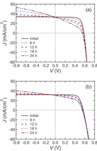
Fig. 3. (Color online) Representative 1-sun-illuminated J–V curves of the modules with (a) (100)- and (b) (111)-oriented p-type c-Si cells before and after the PID tests.
conducted under dark and 1-sun-illuminated conditions for the modules before and after the PID tests. The saturation current density J0, the parallel resistance Rp, and the ideality factor
n were determined by fitting the dark J–V data to the following single-diode equation: J(V)= J0 { exp [ q(V − JRs) nkT ] − 1 } + V− JRs Rp , (1)
where q is the elementary charge, Rs the series resistance, k the Boltzmann constant, and
T the absolute temperature. Here, we did not restrict n to ≤ 2, since n > 2 has often been
observed in PID-affected p-type c-Si PV modules.5, 11) J0, Rp, and Rswere restricted only to
>0. Single-diode fitting was performed with the statistical software Igor Pro 6 (WaveMetrics, Inc.).
3. Results and discussion
Figure 3 shows the representative 1-sun-illuminated J–V curves for the modules with (100)-and (111)-oriented cells before (100)-and after the PID tests. The J–V characteristics shown in Fig. 3 were obtained from the modules with median Pmax/Pmax,0 values after the PID test
per-Fig. 4. (Color Online) Dependences of the normalized maximum powers Pmax/Pmax,0of the modules with (100)- and (111)-oriented cells on PID stress duration. Each data point shows the mean for three modules, and each error bar corresponds to the standard error of the mean.
formed for 24 h, where Pmaxis the maximum power and Pmax,0is the initial maximum power.
Both modules with (100)- and (111)-oriented cells show the typical degradation behavior of the J–V curves characterized by shunting with sublinear characteristics under reverse bias after the PID tests.
Figure 4 shows the dependences of the normalized maximum powers Pmax/Pmax,0 of the
modules fabricated using the (100)- and (111)-oriented cells on PID stress duration. As can be seen in Fig. 4, the Pmax/Pmax,0 values of both (100) and (111) modules decrease with
PID stress duration, demonstrating that PID occurs regardless of surface orientation. The decrease in the Pmax/Pmax,0 of the modules with the (100)-oriented cells is, however, more
significant than that of the modules with the (111)-oriented cells. The Pmax/Pmax,0 values of
the (100)- and (111)-oriented cell modules decreased to about 0.44 and 0.70 after the PID test, respectively. This implies that the PID behavior of p-type c-Si PV modules depends on the surface orientation of the cells, and cells with the (111) surface orientation have higher PID resistance than those with the (100) surface orientation.
Figure 5 shows the dependences of the J0, n, and 1000/Rpof the modules with the (100)
and (111) cells on PID stress duration. The J0, n, and 1000/Rp of the (100) modules are
increased by PID stress more significantly, compared with those of the (111) modules. In particular, inverse Rp has a clear dependence on the surface orientation of the cells. This
indicates that the cells with a (111)-oriented surface tend to be less influenced by shunts caused by PID stress than those with the (100)-oriented surface. PID-affected modules show significantly high n values exceeding 2, as shown in Fig. 5. These high n values have been
Fig. 5. (Color Online) Dependences of J0, n, and 1000/Rpvalues of the modules with (100)- and
(111)-oriented cells on PID stress duration. Each data point shows the mean for three modules, and each error bar corresponds to the standard error of the mean. Note that we do not restrict n values to≤2. Note that the 1000/Rpvalues for (111)-oriented cell modules were almost the same and their error bars were negligible.
observed in the PID of c-Si PV modules5, 11) and originate from a significantly high defect
density in the depletion region introduced by PID stress.10) We can observe that n > 2 in
the unaffected (111)-oriented cell modules. Note that regions damaged by laser cutting or diamond scratching produce n values higher than 2.33) Our solar cells have edge regions damaged during edge isolation using sandpaper. From this, the high n values of the unaffected modules may be attributed to recombination in damaged edge regions.
Fig. 6. Sheet resistances of n+emitters formed on c-Si substrates with different surface orientations. These n+–p junctions were fabricated under the conditions same as those under which the solar cells were fabricated. Sheet resistance was measured by the four point-probe method at room temperature. Each data point shows the mean for three samples, and each error bar corresponds to the standard error of the mean.
Fig. 7. (Color online) D-SIMS profiles of P atoms in the (100) and (111) substrates with a median of sheet resistance. The profiles were obtained using a Cs+primary ion beam with an acceleration voltage of 15 kV.
penetrating the n+emitter of solar cells.10)These Na-decorated stacking faults behave as elec-trically conductive two-dimensional layers that can cause the short-circuiting of the p–n junc-tion.12)On the basis of these facts, PID behavior can be related to the number of such
stack-ing faults penetratstack-ing the n+emitter of the solar cells. First, we should therefore consider the depth of the p–n junction formed by phosphorus diffusion, since an increased junction depth lowers the number of intrinsic stacking faults that can penetrate the n+ emitter of cells. Ac-tually, Berghold et al.2)have reported that the PID of c-Si PV modules depends on the sheet resistance of n+emitters. As shown in Fig. 6, we were not able to observe a clear difference between the sheet resistances of the n+ emitters on the (100) and (111) substrates; however, the sheet resistance of the (111)-oriented substrates was slightly lower than that of the
(100)-with the median sheet resistance is slightly deeper. This slightly deeper junction of the (111)-oriented substrates might cause a higher PID resistance. However, the findings of Berghold
et al.2) imply that the PID resistance does not strongly depend on the sheet resistance of n+
emitters below 55 Ω/sq. Thus, we can probably neglect the effects of the differences in sheet resistance and junction depth on the PID resistance of the modules. Moreover, according to a previous study,34) the diffusion coefficients of P in Si(100) and Si(111) are almost the same,
and the difference in junction depth obtained may not be significant. We therefore have to discuss the effects of other factors on PID behavior.
We consider the number of intrinsic stacking faults in unaffected cells as the second can-didate. One lattice point is included in four {111}-related planes. In (100) substrates, these four types of planes can penetrate the p–n junction. On the other hand, in (111) substrates, one of the four planes does not penetrate the p–n junction, since it is parallel to the p–n junction interface. Assuming that intrinsic stacking faults are generated with the same prob-ability per {111}-related plane, fewer PID-related stacking faults exist in (111) cells than in (100) cells. This can be one reason for the higher PID resistance of the c-Si PV modules with the (111)-oriented cells. Much additional work is, however, required to elucidate this phenomenon.
In a previous study,27)it has been shown that groove-rounded textured cells have a higher PID resistance. This cannot be explained by our experimental results, since the results show that the modules with (111)-oriented flat cells offer a higher PID resistance and, on the basis of the results, we predict that the PID resistance of groove-rounded textured cells will be rather low. Hence, we have to consider other factors for the higher PID resistance of groove-rounded textured cell modules.
We show three possible reasons for the change in the PID resistance of groove-rounded cells as follows: One may be thicker ARC layers covering their grooves. Figure 8 shows schematic diagrams of the ARC films on sharp and rounded grooves. Generally, ARC lay-ers are formed by CVD through the decomposition of source gases and the reaction of the generated radicals. Given that the numbers of radicals supplied to the groove regions are equivalent, the effective thickness of the ARC layer on the rounded grooves becomes larger
Fig. 8. (Color Online) Schematic diagrams of ARC films on (a) the sharp-shaped and (b) the rounded grooves.
than that on the sharp grooves, as illustrated in Fig. 8. The thicker the ARC layer, the weaker the electric field in the layer, and the longer the distance to the emitter surface from the ARC surface. The relatively thicker ARC layers on the rounded grooves might therefore provide higher PID resistance. The second reason may be a smaller surface area. The above results of the dependence on surface orientation were obtained for the substrates with the same surface area. However, the surface area of the groove-rounded cells is slightly smaller than that of the conventional textured cells. Hence, the number of PID-related stacking faults that termi-nate at the Si surface may decrease with decreasing surface area of the grooves. This might result in a slightly higher PID resistance of groove-rounded cells. The last reason may be the change in an electric field around the surface. Smoother and slightly shallower textured surfaces cause change in the electric field distribution around surfaces during PID stressing. This might affect the PID resistance of the cells; however, the effect of the electric field dis-tribution on PID resistance has not yet been investigated in detail. At the present stage, we cannot quantitatively discuss these effects.
4. Conclusions
In this work, by the PID acceleration test, we have investigated the dependence of the surface orientations of flat c-Si cells on PID behavior. The results have demonstrated that the Rp of
the rounded grooves and/or the smaller surface area at the front of the cells.
Acknowledgments
This work was partially supported by New Energy and Industrial Technology Development Organization (NEDO). We would like to thank Dr. Kohjiro Hara and Sachiko Jonai of AIST for their helpful advice on the module lamination. We would also like to thank Dr. Shuhei Yoshiba of Japan Science and Technology Agency (JST) for his helpful advice on the co-firing process. We would also like to thank Chie Yamamoto of JAIST for her assistance.
References
1) S. Pingel, O. Frank, M. Winkler, S. Daryan, T. Geipel, H, Hoehne, and J. Berghold, Proc. 35th IEEE Photovoltaic Specialists Conf., 2010, p. 2817.
2) J. Berghold, O. Frank, H. Hoehne, S. Pingel, B. Richardson, and M. Winkler, Proc. 25th European Photovoltaic Solar Energy Conf. Exhib./5th World Conf. Photovoltaic Energy Conversion, 2010, p. 3753.
3) P. Hacke, M. Kempe, K. Terwilliger, S. Glick, N. Call, S. Johnston, S. Kurtz, I. Bennett, and M. Kloos, Proc. 25th European Photovoltaic Solar Energy Conf. Exhib./ 5th World Conf. Photovoltaic Energy Conversion, 2010, p. 3760.
4) P. Hacke, K. Terwilliger, R. Smith, S. Glick, J. Pankow, M. Kempe, S. Kurtz, I. Bennett, and M. Kloos, Proc. 37th IEEE Photovoltaic Specialists Conf., 2011, p. 814. 5) C. Taubitz, M. Sch¨utze, and M. B. Koentopp, Proc. 27th European Photovoltaic Solar
Energy Conf. Exhib., 2012, p. 3172.
6) V. Naumann, C. Hagendorf, S. Grosser, M. Werner, and J. Bagdahn, Energy Procedia 27, 1 (2012).
7) J. Bauer, V. Naumann, S. Großer, C. Hagendorf, M. Sch¨utze, and O. Breitenstein, Phys. Status Solidi: Rapid Res. Lett. 6, 331 (2012).
8) V. Naumann, D. Lausch, S. Großer, M. Werner, S. Swatek, C. Hagendorf, and J. Bagdahn, Energy Procedia 33, 76 (2013).
9) V. Naumann, D. Lausch, A. Graff, M. Werner, S. Swatek, J. Bauer, A. H¨ahnel, O. Breitenstein, S. Großer, J. Bagdahn, and C. Hagendorf, Phys. Status Solidi: Rapid Res. Lett. 7, 315 (2013).
10) V. Naumann, D. Lausch, A. H¨ahnel, J. Bauer, O. Breitenstein, A. Graff, M. Werner, S. Swatek, S. Großer, J. Bagdahn, and C. Hagendorf, Sol. Energy Mater. Sol. Cells 120, 383 (2014).
11) D. Lausch, V. Naumann, O. Breitenstein, J. Bauer, A. Graff, J. Bagdahn, and C. Hagendorf, IEEE J. Photovoltaics 4, 834 (2014).
12) B. Ziebarth, M. Mrovec, C. Els¨asser, and P. Gumbsch, J. Appl. Phys. 116, 093510 (2014).
13) M. Wilson, A. Savtchouk, P. Edelman, D. Marinskiy, and J. Lagowski, Sol. Energy Mater. Sol. Cells 142, 102 (2015).
14) M. Kambe, K. Hara, K. Mitarai, S. Takeda, M. Fukawa, N. Ishimaru, and M. Kondo, Proc. 28th European Photovoltaic Solar Energy Conf. Exhib., 2013 p. 2861,
18) J. Kapur, K. M. Stika, C. S. Westphal, J. L. Norwood, and B. Hamzavytehrany, IEEE J. Photovoltaics 5, 219 (2015).
19) S. Jonai, K. Hara, Y. Tsutsui, H. Nakahama, and A. Masuda, Jpn. J. Appl. Phys. 54, 08KG01 (2015).
20) H. Nagel, A. Metz, and K. Wangemann, Proc. 26th European Photovoltaic Solar Energy Conf. Exhib., 2011, p. 3107.
21) S. Koch, D. Nieschalk, J. Berghold, S. Wendlandt, S. Krauter, and P. Grunow, Proc. 27th European Photovoltaic Solar Energy Conf. Exhib., 2012, p. 1985.
22) K. Mishina, A. Ogishi, K. Ueno, T. Doi, K. Hara, N. Ikeno, D. Imai,T. Saruwatari, M. Shinohara, T. Yamazaki. A. Ogura, Y. Ohshita, and A. Masuda, Jpn. J. Appl. Phys. 53, 03CE01 (2014).
23) K. Mishina, A. Ogishi, K. Ueno, S. Jonai, N. Ikeno, T. Saruwatari, K. Hara, A. Ogura, T. Yamazaki, T. Doi, M. Shinohara, and A. Masuda, Jpn. J. Appl. Phys. 54, 08KD12 (2015).
24) K. Hara, H. Ichinose, T. Murakami, and A. Masuda, RSC Adv. 4, 44291 (2014).
25) C.-H. Du, C.-H. Chen, C.-H. Lung, S.-Y. Chen, L.-Y. Li, Y.-H. Lin, and J. A. Yeh, ECS J. Solid State Sci. Technol. 4, 97 (2015).
26) D. Lausch, V. Naumann, A. Graff, A. H¨ahnel, O. Breitenstein, C. Hagendorf, and J. Bagdahn, Energy Procedia 55, 486 (2014).
27) Y.-C. Chen C.-C. Wang, S.-H. Yang, Y.-H. Wang, C.-T. Tsai, K.-C. Lin, G.-F. Chen, and W. K. W. Huang, presented at 2014 NREL Photovoltaic Module Reliability Workshop, 2014.
28) A. Masuda, H. Umemoto, and H. Matsumura, Thin Solid Films 501, 149 (2006). 29) A. Hauser, G. Hahn, M. Spiegel, H. Feist, O. Breitenstein, J. P. Rakotoniaina, P. Fath,
and E. Bucher, Proc. 17th European Photovoltaic Solar Energy Conf. Exhib., 2001, p. 1739.
30) S. Yamaguchi, S. Jonai, K. Hara, H. Komaki, Y. Shimizu-Kamikawa, H. Shibata, S. Niki, Y. Kawakami, and A. Masuda, Jpn. J. Appl. Phys. 54, 08KC13 (2015). 31) S. Hoffmann and M. Koehl, Prog. Photovoltaics 22, 173 (2014).
32) K. Hara, S. Jonai, and A. Masuda, Sol. Energy Mater. Sol. Cells 140, 361 (2015). 33) S. Steingrube, O. Breitenstein, K. Ramspeck, S. Glunz, A. Schenk, and P. P. Altermatt,
J. Appl. Phys. 110, 014515 (2011).