はじめに
• 講義資料:大槻東巳のホームページ,講義資料からダウ
ンロードする
• 今日の授業と資料を基に1月29日までにA4用紙1枚でレ
ポートを作成。課題は
トポロジカル絶縁体とは何か?
• 提出先:4-389A
トポロジカル絶縁体入門
物理学序論
上智大学物理領域
大槻東巳
2016年のノーベル物理学賞
サウレス
ハルデイン
コスタリッツ
½ ¼ ¼
トポロジー
https://www.nobelprize.org/nobel_prizes/physics/laureates/2016/fig_fy_en_
16_topology.pdf
アウトライン
• トポロジカル絶縁体(topological insulator, TI)とは何か?
• 昔から知られていたトポロジカル絶縁体 : 量子ホール効果
(QHE)における量子ホール絶縁体quantum Hall insulator (QHI)
• 量子ホール絶縁体以外のトポロジカル絶縁体の予言と発見 à
2次元量子スピンホール系 (quantum spin Hall systems
(QSHE)(HgTe))と3次元 TI (Bi
2
Se
3
)
• CdTe/HgTe/CdTe量子井戸における量子スピンホール効果
• GaN/InN/GaN量子井戸の可能性
References :
1) 東北大学金属材料研 野村健太郎准教授による講義ノート
http://www-lab.imr.tohoku.ac.jp/~nomura/note.html
2) Review: M. Hasan, C. Kane: Rev. Mod. Phys. 82 (2010) 3045
3) Review: X.-L. Qi, S.-C. Zhang: Rev. Mod. Phys. 83 (2011) 1057
4) Miao et al., Topological Insulator Transition in a GaN/InN/GaN Quantum Well,
PRL 109, 186803 (2012)
5) Photonic topological insulator 1: Haldane, Raghu: PRL 100, 013904 (2008)
6) Photonic topological insulator 2: Khanikaev et al.: Nature materials, 12
1. トポロジカル絶縁体とは ?
•
バンドギャップ絶縁体でギャップ内に端
/
表
面状態をもつもの。
•
ただの表面状態でなく,トポロジカルな要因
で保護されているため,ランダムネス,電子
間相互作用,電子格子相互作用の影響を受け
ない。
•
電流やスピンの方向が特徴的
2. 昔から知られていたトポロジカル絶
縁体,
QHI in QHE
@>)#$>= A)** %--%($
4*"$'"#+B C,12) )#2 D%??%1 EFGHI
2
1
1, 2,3,
j
h
R
j
j e
@>)#$>= A)** %--%($
4*"$'"#+B C,12) )#2 D%??%1 EFGHI
2
1
1, 2,3,
j
h
R
j
j e
σ
yx
=
e
2
h
j ,
σ
xx
= 0
絶縁体
異なるタイプの絶縁相
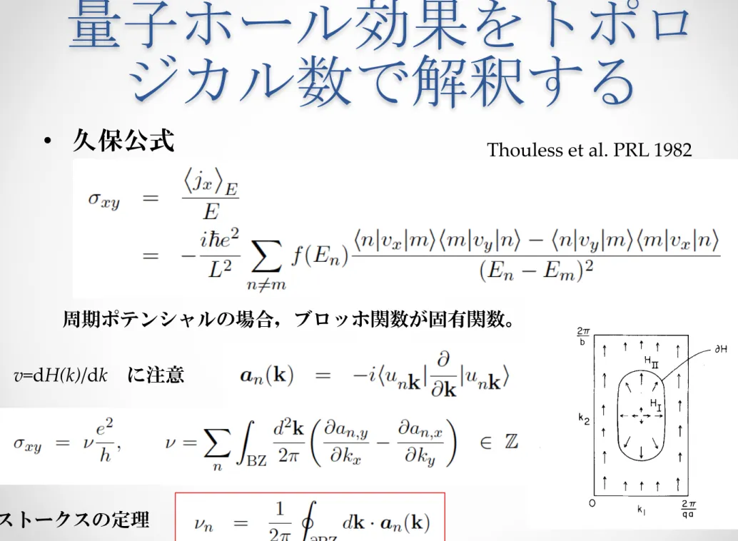
量子ホール効果をトポロ
ジカル数で解釈する
• 久保公式
周期ポテンシャルの場合,ブロッホ関数が固有関数。
ストークスの定理
TOPOLOGY OF HALL CONDUCTANCE
349
tity remains invariant under this transformation.
From Eq. (3.8) the corresponding
transformation of ji(k,, k2) is given by
A’@, , kd = &k,, kz) + zV,f(k,, k,).
(3.11)
It is easy to see from Eqs. (3.9) and (3.11) that og is invariant under the transfor-
mation (3.10).
The non-trivial topology arises when the phase of the wavefunction cannot be
determined uniquely and smoothly in the entire magnetic Brillouin zone. The
transformation
(3.10) implies that the overall phase factor for each state vector
1 uklk2) can be chosen arbitrary. This phase can be determined, for example, by
demanding that a component of the state vector u~,,Jx(~), y”‘) = (x(O), ~“‘1 uklk2) is
real. However, this convention is not enough to fix the phase on the entire magnetic
Brillouin zone, since z.Q&x’~), y(O)) vanishes for some (k,, k2). The existence of
zeros of z+,,Jx, y) has been shown in Section II. For the sake of simplicity, consider
the case where u,,,,(x(~), y(O)) vanishes only at one point (k\“, kh”) in the magnetic
Brillouin zone. See Fig. 1. Divide T2 into two pieces HI and H,, such that H, con-
tains (k!O), k$O)). We adopt a different convention in H, so that another component
of the state vector z.++(x’~), y”)) = (x’~‘, y”‘] u~,~,) is real, where (x(l), y(l)) and H,
are chosen such that LQ,,~~(x(‘), y’“) does not vanish in H,. Thus the overall phase
is uniquely determined on the entrie T*. In Fig. 1, a phase of one component of the
state vector u~,~~(x”‘, y(O)) = (.~~O’y(‘)l uklk2) is schematically drawn.
IT rtt
T
0
kl - 27T qa
FIG. 1. Schematic diagram of a phase of a wavefunction in the magnetic Brillouin zone. The Brillouin zone is actually a torus, so the edges (k,, kZ) = (0, k2) and (2z/qa, k,); and also the edges (k, . 0) and (k, , 2x/b) must be identified.
Thouless et al. PRL 1982
量子ホール効果から得ら
れた教訓
• バルクの波動関数が非自明な位相構造を持つ à この位相構
造をトポロジカル数で定義
à 量子ホールコンダクタンスは
e
2
/h x トポロジカル数となり厳密に量子化
• トポロジカル数は整数のみを取るので,ある程度の摂動を受
けてもコンダクタンスは変化しない
à
10
-9
の精度で量子化
• この議論の弱点:トポロジカル数はブロッホ関数で定義され
ているが,量子ホール効果は乱れた
2次元電子系で観測され
ている
バルク
vs. エッジ描像
• バルクのトポロジカル数が
nの場合,
n本のエッジ状態
がサンプルの端に現れる。
• àバルクの波動関数のトポロジーをトポロジカル数
(Chern number)で定義する代わりに,実験的には試料
のエッジ状態を調べればよい
http://physics.aps.org/articles/v2/15
エッジ描像の利点
• エッジ電流は電流測定に直接きいてくる
• ランダムネスがあっても定義できる
• エッジ状態がランダムネス・相互作用に対して安定かど
うかはある程度直感的に分かる
3. 量子ホール絶縁体以外の
トポロジカル絶縁体に向けて
• 量子ホール効果の発見1980年,分数量子ホール効果が
1982年,それぞれにノーベル賞が授与され済み
•
2000年代前半 à スピントロニクスの研究の発展
o 電流ではなく,スピンを流したい。しかも磁石や磁場を使わず
•
2次元系でスピンを流す:時間反転対称性のある量子
ホール効果
à 量子
スピン
ホール効果(
QSHE)
•
2010年前後:3次元のトポロジカル絶縁体
• いずれもスピン軌道相互作用がキー
実際の物質
o 2D HgTe QSHE 後で詳しく述べる
o 3D
•
Bi
2
Se
3
(2009, Yu-Qi Xia, Zahid Hasan),
•
Bi
0.9
Sb
0.1
(2008, David Hsieh, Zahid Hasan)
•
Bi
2
Te
3
•
TlBiSe
2
H Zhang et al., Nature Physics, 2009
With randomness
ARPES
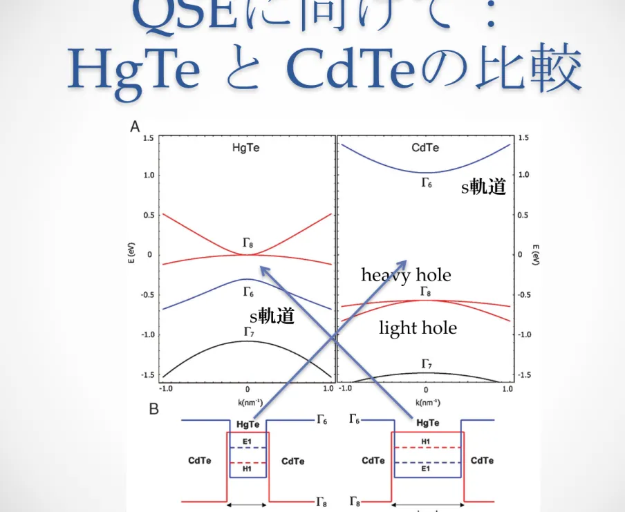
QSEに向けて:
HgTe と CdTeの比較
1D gapless edge states that lie inside the bulk insulating gap.
The edge states have a distinct helical property: Two states
with opposite spin polarization counterpropagate at a given
edge (
Kane and Mele, 2005a
;
Wu
et al., 2006
;
Xu and
Moore, 2006
). For this reason they are also called helical
edge states, i.e., the spin is correlated with the direction of
motion (
Wu et al., 2006
). The edge states come in Kramers
doublets, and TR symmetry ensures the crossing of their
energy levels at special points in the Brillouin zone (BZ).
Because of this level crossing, the spectrum of a QSH
insu-lator cannot be adiabatically deformed into that of a
topo-logically trivial insulator without helical edge states.
Therefore, in this sense, the QSH insulator represents a new
topologically distinct state of matter. In the special case that
SOC preserves a U
ð1Þ
s
subgroup of the full SU(2) spin
rotation group, the topological properties of the QSH state
can be characterized by the spin Chern number (
Sheng et al.,
2006
). More generally, the topological properties of the QSH
state are mathematically characterized by a
Z
2
topological
invariant (
Kane and Mele, 2005b
). States with an even
num-ber of Kramers pairs of edge states at a given edge are
topologically trivial, while those with an odd number are
topologically nontrivial. The
Z
2
topological quantum number
can also be defined for generally interacting systems and
experimentally measured in terms of the fractional charge
and quantized current on the edge (
Qi, Hughes, and Zhang,
2008a
), and spin-charge separation in the bulk (
Qi and Zhang,
2008
;
Ran et al., 2008
).
In this section, we focus on the basic theory of the QSH
state in the HgTe/CdTe system because of its simplicity and
experimental relevance and provide an explicit and
pedagog-ical discussion of the helpedagog-ical edge states and their transport
properties. There are several other theoretical proposals for
the QSH state, including bilayer bismuth (
Murakami, 2006
),
and the ‘‘broken-gap’’ type-II AlSb/InAs/GaSb quantum
wells (
Liu, Hughes et al., 2008
). Initial experiments in the
AlSb/InAs/GaSb system already show encouraging
signa-tures (
Knez et al., 2010
). The QSH system has also been
proposed for the transition metal oxide Na
2
IrO
3
(
Shitade
et al., 2009
). The concept of the fractional QSH state was
proposed at the same time as the QSH state (
Bernevig and
Zhang, 2006
) and has been recently investigated theoretically
in more detail (
Young et al., 2008
;
Levin and Stern, 2009
).
A. Effective model of the two-dimensional
time-reversal-invariant topological insulator
in HgTe/CdTe quantum wells
In this section we review the basic electronic structure of
bulk HgTe and CdTe and presented a simple model first
introduced by
Bernevig, Hughes, and Zhang (2006)
(BHZ)
to describe the physics of those subbands of HgTe/CdTe
quantum wells which are relevant for the QSH effect. HgTe
and CdTe crystallize in the zinc blende lattice structure. This
structure has the same geometry as the diamond lattice, i.e.,
two interpenetrating face-centered-cubic lattices shifted
along the body diagonal, but with a different atom on each
sublattice. The presence of two different atoms per lattice site
breaks inversion symmetry and thus reduces the point group
symmetry from O
h
(cubic) to T
d
(tetrahedral). However, even
though inversion symmetry is explicitly broken, this has only
a small effect on the physics of the QSH effect. To simplify
the discussion, we first ignore this bulk inversion asymmetry
(BIA).
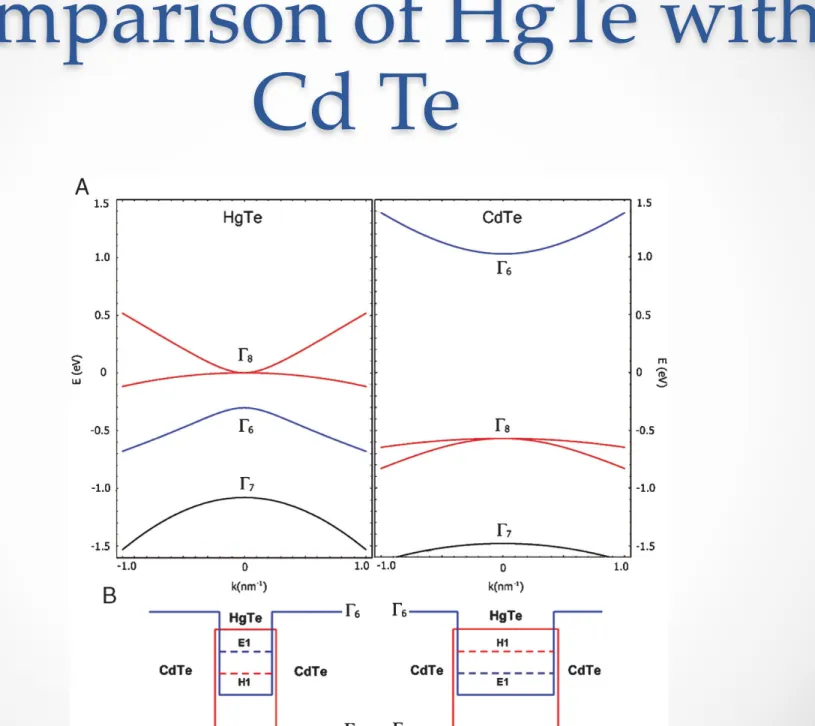
For both HgTe and CdTe, the important bands near the
Fermi level are close to the ! point in the Brillouin zone
[Fig.
2(a)
]. They are a s-type band (!
6
), and a p-type band
split by SOC into a J
¼ 3=2 band (!
8
) and a J
¼ 1=2 band
(!
7
). CdTe has a band ordering similar to GaAs with a s-type
(!
6
) conduction band, and p-type valence bands (!
8
, !
7
)
which are separated from the conduction band by a large
energy gap (
$ 1:6 eV). Because of the large SOC present in
the heavy element Hg, the usual band ordering is inverted :
The negative energy gap of
%300 meV indicates that the !
8
band, which usually forms the valence band, is above the !
6
band. The light-hole !
8
band becomes the conduction band,
the heavy-hole band becomes the first valence band, and the
s-type band (!
6
) is pushed below the Fermi level to lie
between the heavy-hole band and the spin-orbit split-off
band (!
7
) [Fig.
2(a)
]. Because of the degeneracy between
heavy-hole and light-hole bands at the ! point, HgTe is a
zero-gap semiconductor.
When HgTe-based quantum well structures are grown, the
peculiar properties of the well material can be utilized to
tune the electronic structure. For wide QW layers, quantum
confinement is weak and the band structure remains inverted.
However, the confinement energy increases when the well
width is reduced. Thus, the energy levels will be shifted and,
eventually, the energy bands will be aligned in a ‘‘normal’’
way, if the QW thickness d
QW
falls below a critical thickness
d
c
. We can understand this heuristically as follows: for thin
QWs the heterostructure should behave similarly to CdTe
and have a normal band ordering, i.e., the bands with
primarily !
6
symmetry are the conduction subbands and
FIG. 2 (color).
(a) Bulk band structure of HgTe and CdTe;
(b) schematic picture of quantum well geometry and lowest
sub-bands for two different thicknesses. From
Bernevig et al., 2006
.
Xiao-Liang Qi and Shou-Cheng Zhang: Topological insulators and superconductors
1061
Rev. Mod. Phys., Vol. 83, No. 4, October–December 2011
s軌道
heavy hole
light hole
s軌道
Hamiltonian
s-orbital: Kramers doublet |s↑> and |s ↓>
p-orbital: |p
x
+ i p
y
↑>, |-(p
x
- i p
y
) ↓>
Near the Γ point: |s+>, |p
x
+ i p
y
↑>, |s->, |-(p
x
- i p
y
) ↓>
E(k)
=
ε
(k)
± (M − Bk
2
)
2
+ A
2
k
2
(
Science ‘06)
H(k), 2x2行列
sとpの間のエネルギーM
を変えると
M>0
M=0
M<0
s
p
s
p
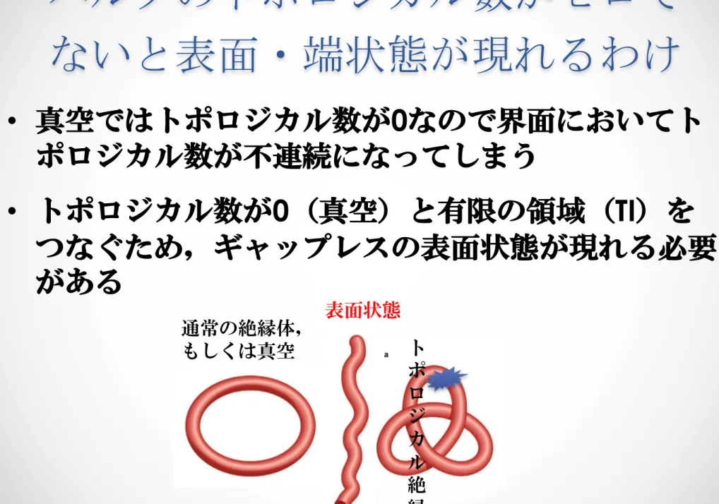
エッジ状態はなぜ安定か?
(ランダムネス,相互作用などに対して)
バルクのトポロジカル数がゼロで
ないと表面・端状態が現れるわけ
•
真空ではトポロジカル数が
0
なので界面においてト
ポロジカル数が不連続になってしまう
•
トポロジカル数が
0
(真空)と有限の領域(
TI
)を
つなぐため,ギャップレスの表面状態が現れる必要
がある
a b a bsymmetry as an applied magnetic field would), in simplified models introduced in around 2003 it can lead to a quantum spin Hall effect, in which electrons with opposite spin angular momentum (commonly called spin up and spin down) move in opposite directions around the edge of the droplet in the absence of an external magnetic field2 (Fig. 2b).
These simplified models were the first steps towards understanding topological insulators. But it was unclear how realistic the models were: in real materials, there is mixing of spin-up and spin-down electrons, and there is no conserved spin current. It was also unclear whether the edge state of the droplet in Fig. 2b would survive the addition of even a few impurities.
In 2005, a key theoretical advance was made by Kane and Mele3.
They used more realistic models, without a conserved spin current, and showed how some of the physics of the quantum spin Hall effect can survive. They found a new type of topological invariant that could be computed for any 2D material and would allow the prediction of whether the material had a stable edge state. This allowed them to show that, despite the edge not being stable in many previous models, there are realistic 2D materials that would have a stable edge state in the absence of a magnetic field; the resultant 2D state was the first topological insulator to be understood. This non-magnetic insulator has edges that act like perfectly conducting one-dimensional electronic wires at low tempera-tures, similar to those in the quantum Hall effect.
Subsequently, Bernevig, Hughes and Zhang made a theoretical prediction that a 2D topological insulator with quantized charge con-ductance along the edges would be realized in (Hg,Cd)Te quantum wells4. The quantized charge conductance was indeed observed in this
system, as a quantum-Hall-like plateau in zero magnetic field, in 2007 (ref. 5). These experiments are similar to those on the quantum Hall effect in that they require, at least so far, low temperature and artificial 2D materials (quantum wells), but they differ in that no magnetic field is needed.
Going 3D
The next important theoretical development, in 2006, was the realization6–8 that even though the quantum Hall effect does not
general-ize to a genuinely 3D state, the topological insulator does, in a subtle way. Although a 3D ‘weak’ topological insulator can be formed by layering 2D versions, similar to layered quantum Hall states, the resultant state is not stable to disorder, and its physics is generally similar to that of the 2D state. In weak topological insulators, a dislocation (a line-like defect
in the crystal) will always contain a quantum wire like that at the edge of the quantum spin Hall effect (discussed earlier), which may allow 2D topological insulator physics to be observed in a 3D material9.
There is also, however, a ‘strong’ topological insulator, which has a more subtle relationship to the 2D case; the relationship is that in two dimensions it is possible to connect ordinary insulators and topologi-cal insulators smoothly by breaking time-reversal symmetry7. Such a
continuous interpolation can be used to build a 3D band structure that respects time-reversal symmetry, is not layered and is topologically non-trivial. It is this strong topological insulator that has protected metallic surfaces and has been the focus of experimental activity.
Spin–orbit coupling is again required and must mix all components of the spin. In other words, there is no way to obtain the 3D strong topologi-cal insulator from separate spin-up and spin-down electrons, unlike in the 2D case. Although this makes it difficult to picture the bulk physics of the 3D topological insulator (only the strong topological insulator will be discussed from this point), it is simple to picture its metallic surface6.
The unusual planar metal that forms at the surface of topological insulators ‘inherits’ topological properties from the bulk insulator. The simplest manifestation of this bulk–surface connection occurs at a smooth surface, where momentum along the surface remains well defined: each momentum along the surface has only a single spin state at the Fermi level, and the spin direction rotates as the momentum moves around the Fermi surface (Fig. 3). When disorder or impurities are added at the surface, there will be scattering between these surface states but, crucially, the topological properties of the bulk insulator do not allow the metallic surface state to vanish — it cannot become local-ized or gapped. These two theoretical predictions, about the electronic structure of the surface state and the robustness to disorder of its metallic behaviour, have led to a flood of experimental work on 3D topological insulators in the past two years.
Experimental realizations
The first topological insulator to be discovered was the alloy BixSb1−x,
the unusual surface bands of which were mapped in an angle-resolved photoemission spectroscopy (ARPES) experiment10,11. In ARPES
exper-iments, a high-energy photon is used to eject an electron from a crystal, and then the surface or bulk electronic structure is determined from an analysis of the momentum of the emitted electron. Although the surface structure of this alloy was found to be complex, this work launched a search for other topological insulators.
Figure 1 | Metallic states are born when a surface unties ‘knotted’ electron wavefunctions. a, An illustration of topological change and the resultant surface state. The trefoil knot (left) and the simple loop (right) represent different insulating materials: the knot is a topological insulator, and the loop is an ordinary insulator. Because there is no continuous deformation by which one can be converted into the other, there must be a surface where the string is cut, shown as a string with open ends (centre), to pass between the two knots; more formally, the topological invariants cannot remain
defined. If the topological invariants are always defined for an insulator, then the surface must be metallic. b, The simplest example of a knotted 3D electronic band structure (with two bands)35, known to mathematicians as the Hopf map. The full topological structure would also have linked fibres on each ring, in addition to the linking of rings shown here. The knotting in real topological insulators is more complex as these require a minimum of four electronic bands, but the surface structure that appears is relatively simple (Fig. 3).
195
NATURE|Vol 464|11 March 2010
PERSPECTIVE
INSIGHT
194-198 Insight Moore NS.indd 195
194-198 Insight Moore NS.indd 195 3/3/10 11:30:563/3/10 11:30:56
© 20 Macmillan Pu blishers Limited. All rights reserved10
a b
a b
symmetry as an applied magnetic field would), in simplified models introduced in around 2003 it can lead to a quantum spin Hall effect, in which electrons with opposite spin angular momentum (commonly called spin up and spin down) move in opposite directions around the edge of the droplet in the absence of an external magnetic field2 (Fig. 2b).
These simplified models were the first steps towards understanding topological insulators. But it was unclear how realistic the models were: in real materials, there is mixing of spin-up and spin-down electrons, and there is no conserved spin current. It was also unclear whether the edge state of the droplet in Fig. 2b would survive the addition of even a few impurities.
In 2005, a key theoretical advance was made by Kane and Mele3.
They used more realistic models, without a conserved spin current, and showed how some of the physics of the quantum spin Hall effect can survive. They found a new type of topological invariant that could be computed for any 2D material and would allow the prediction of whether the material had a stable edge state. This allowed them to show that, despite the edge not being stable in many previous models, there are realistic 2D materials that would have a stable edge state in the absence of a magnetic field; the resultant 2D state was the first topological insulator to be understood. This non-magnetic insulator has edges that act like perfectly conducting one-dimensional electronic wires at low tempera-tures, similar to those in the quantum Hall effect.
Subsequently, Bernevig, Hughes and Zhang made a theoretical prediction that a 2D topological insulator with quantized charge con-ductance along the edges would be realized in (Hg,Cd)Te quantum wells4. The quantized charge conductance was indeed observed in this
system, as a quantum-Hall-like plateau in zero magnetic field, in 2007 (ref. 5). These experiments are similar to those on the quantum Hall effect in that they require, at least so far, low temperature and artificial 2D materials (quantum wells), but they differ in that no magnetic field is needed.
Going 3D
The next important theoretical development, in 2006, was the realization6–8 that even though the quantum Hall effect does not
general-ize to a genuinely 3D state, the topological insulator does, in a subtle way. Although a 3D ‘weak’ topological insulator can be formed by layering 2D versions, similar to layered quantum Hall states, the resultant state is not stable to disorder, and its physics is generally similar to that of the 2D state. In weak topological insulators, a dislocation (a line-like defect
in the crystal) will always contain a quantum wire like that at the edge of the quantum spin Hall effect (discussed earlier), which may allow 2D topological insulator physics to be observed in a 3D material9.
There is also, however, a ‘strong’ topological insulator, which has a more subtle relationship to the 2D case; the relationship is that in two dimensions it is possible to connect ordinary insulators and topologi-cal insulators smoothly by breaking time-reversal symmetry7. Such a
continuous interpolation can be used to build a 3D band structure that respects time-reversal symmetry, is not layered and is topologically non-trivial. It is this strong topological insulator that has protected metallic surfaces and has been the focus of experimental activity.
Spin–orbit coupling is again required and must mix all components of the spin. In other words, there is no way to obtain the 3D strong topologi-cal insulator from separate spin-up and spin-down electrons, unlike in the 2D case. Although this makes it difficult to picture the bulk physics of the 3D topological insulator (only the strong topological insulator will be discussed from this point), it is simple to picture its metallic surface6.
The unusual planar metal that forms at the surface of topological insulators ‘inherits’ topological properties from the bulk insulator. The simplest manifestation of this bulk–surface connection occurs at a smooth surface, where momentum along the surface remains well defined: each momentum along the surface has only a single spin state at the Fermi level, and the spin direction rotates as the momentum moves around the Fermi surface (Fig. 3). When disorder or impurities are added at the surface, there will be scattering between these surface states but, crucially, the topological properties of the bulk insulator do not allow the metallic surface state to vanish — it cannot become local-ized or gapped. These two theoretical predictions, about the electronic structure of the surface state and the robustness to disorder of its metallic behaviour, have led to a flood of experimental work on 3D topological insulators in the past two years.
Experimental realizations
The first topological insulator to be discovered was the alloy BixSb1−x,
the unusual surface bands of which were mapped in an angle-resolved photoemission spectroscopy (ARPES) experiment10,11. In ARPES
exper-iments, a high-energy photon is used to eject an electron from a crystal, and then the surface or bulk electronic structure is determined from an analysis of the momentum of the emitted electron. Although the surface structure of this alloy was found to be complex, this work launched a search for other topological insulators.
Figure 1 | Metallic states are born when a surface unties ‘knotted’ electron wavefunctions. a, An illustration of topological change and the resultant surface state. The trefoil knot (left) and the simple loop (right) represent different insulating materials: the knot is a topological insulator, and the loop is an ordinary insulator. Because there is no continuous deformation by which one can be converted into the other, there must be a surface where the string is cut, shown as a string with open ends (centre), to pass between the two knots; more formally, the topological invariants cannot remain
defined. If the topological invariants are always defined for an insulator, then the surface must be metallic. b, The simplest example of a knotted 3D electronic band structure (with two bands)35, known to mathematicians as the Hopf map. The full topological structure would also have linked fibres on each ring, in addition to the linking of rings shown here. The knotting in real topological insulators is more complex as these require a minimum of four electronic bands, but the surface structure that appears is relatively simple (Fig. 3).
195
NATURE|Vol 464|11 March 2010
PERSPECTIVE
INSIGHT
194-198 Insight Moore NS.indd 195
194-198 Insight Moore NS.indd 195 3/3/10 11:30:563/3/10 11:30:56
© 20 Macmillan Pu blishers Limited. All rights reserved10
ト
ポ
ロ
ジ
カ
ル
絶
縁
体
通常の絶縁体,
もしくは真空
aa bbsymmetry as an applied magnetic field would), in simplified models introduced in around 2003 it can lead to a quantum spin Hall effect, in which electrons with opposite spin angular momentum (commonly called spin up and spin down) move in opposite directions around the edge of the droplet in the absence of an external magnetic field2 (Fig. 2b).
These simplified models were the first steps towards understanding topological insulators. But it was unclear how realistic the models were: in real materials, there is mixing of spin-up and spin-down electrons, and there is no conserved spin current. It was also unclear whether the edge state of the droplet in Fig. 2b would survive the addition of even a few impurities.
In 2005, a key theoretical advance was made by Kane and Mele3.
They used more realistic models, without a conserved spin current, and showed how some of the physics of the quantum spin Hall effect can survive. They found a new type of topological invariant that could be computed for any 2D material and would allow the prediction of whether the material had a stable edge state. This allowed them to show that, despite the edge not being stable in many previous models, there are realistic 2D materials that would have a stable edge state in the absence of a magnetic field; the resultant 2D state was the first topological insulator to be understood. This non-magnetic insulator has edges that act like perfectly conducting one-dimensional electronic wires at low tempera-tures, similar to those in the quantum Hall effect.
Subsequently, Bernevig, Hughes and Zhang made a theoretical prediction that a 2D topological insulator with quantized charge con-ductance along the edges would be realized in (Hg,Cd)Te quantum wells4. The quantized charge conductance was indeed observed in this
system, as a quantum-Hall-like plateau in zero magnetic field, in 2007 (ref. 5). These experiments are similar to those on the quantum Hall effect in that they require, at least so far, low temperature and artificial 2D materials (quantum wells), but they differ in that no magnetic field is needed.
Going 3D
The next important theoretical development, in 2006, was the realization6–8 that even though the quantum Hall effect does not
general-ize to a genuinely 3D state, the topological insulator does, in a subtle way. Although a 3D ‘weak’ topological insulator can be formed by layering 2D versions, similar to layered quantum Hall states, the resultant state is not stable to disorder, and its physics is generally similar to that of the 2D state. In weak topological insulators, a dislocation (a line-like defect
in the crystal) will always contain a quantum wire like that at the edge of the quantum spin Hall effect (discussed earlier), which may allow 2D topological insulator physics to be observed in a 3D material9.
There is also, however, a ‘strong’ topological insulator, which has a more subtle relationship to the 2D case; the relationship is that in two dimensions it is possible to connect ordinary insulators and topologi-cal insulators smoothly by breaking time-reversal symmetry7. Such a
continuous interpolation can be used to build a 3D band structure that respects time-reversal symmetry, is not layered and is topologically non-trivial. It is this strong topological insulator that has protected metallic surfaces and has been the focus of experimental activity.
Spin–orbit coupling is again required and must mix all components of the spin. In other words, there is no way to obtain the 3D strong topologi-cal insulator from separate spin-up and spin-down electrons, unlike in the 2D case. Although this makes it difficult to picture the bulk physics of the 3D topological insulator (only the strong topological insulator will be discussed from this point), it is simple to picture its metallic surface6.
The unusual planar metal that forms at the surface of topological insulators ‘inherits’ topological properties from the bulk insulator. The simplest manifestation of this bulk–surface connection occurs at a smooth surface, where momentum along the surface remains well defined: each momentum along the surface has only a single spin state at the Fermi level, and the spin direction rotates as the momentum moves around the Fermi surface (Fig. 3). When disorder or impurities are added at the surface, there will be scattering between these surface states but, crucially, the topological properties of the bulk insulator do not allow the metallic surface state to vanish — it cannot become local-ized or gapped. These two theoretical predictions, about the electronic structure of the surface state and the robustness to disorder of its metallic behaviour, have led to a flood of experimental work on 3D topological insulators in the past two years.
Experimental realizations
The first topological insulator to be discovered was the alloy BixSb1−x,
the unusual surface bands of which were mapped in an angle-resolved photoemission spectroscopy (ARPES) experiment10,11. In ARPES
exper-iments, a high-energy photon is used to eject an electron from a crystal, and then the surface or bulk electronic structure is determined from an analysis of the momentum of the emitted electron. Although the surface structure of this alloy was found to be complex, this work launched a search for other topological insulators.
Figure 1 | Metallic states are born when a surface unties ‘knotted’ electron wavefunctions. a, An illustration of topological change and the resultant surface state. The trefoil knot (left) and the simple loop (right) represent different insulating materials: the knot is a topological insulator, and the loop is an ordinary insulator. Because there is no continuous deformation by which one can be converted into the other, there must be a surface where the string is cut, shown as a string with open ends (centre), to pass between the two knots; more formally, the topological invariants cannot remain
defined. If the topological invariants are always defined for an insulator, then the surface must be metallic. b, The simplest example of a knotted 3D electronic band structure (with two bands)35, known to mathematicians as the Hopf map. The full topological structure would also have linked fibres on each ring, in addition to the linking of rings shown here. The knotting in real topological insulators is more complex as these require a minimum of four electronic bands, but the surface structure that appears is relatively simple (Fig. 3).
195
NATURE|Vol 464|11 March 2010 PERSPECTIVE INSIGHT
194-198 Insight Moore NS.indd 195
194-198 Insight Moore NS.indd 195 3/3/10 11:30:563/3/10 11:30:56
© 20 Macmillan Pu blishers Limited. All rights reserved10