集積回路システム工学 第 9 回講義
アナログ集積回路 調査研究事例 ビジョンチップ、抵抗ネットワーク
小林春夫
群馬大学大学院理工学府 電子情報部門 [email protected]
下記から講義使用 pdfファイルをダウンロードしてください。
出席・講義感想もここから入力してください。
https://kobaweb.ei.st.gunma-u.ac.jp/lecture/lecture.html
2021 年 6 月 15 日 ( 火 )
ロサンゼルス地区
738 IEEE JOURNAL OF SOLID-STATE CIRCUITS, VOL. 26, NO. 5, MAY 1991
An Active Resistor Network for Gaussian Filtering of Images
Haruo Kobayashi, Joseph L. White, Student Member, IEEE, and Asad A. Abidi, Member, IEEE
Abstract—The architecture of an active resistive mesh con- taining both positive and negative resistors to implement a Gaussian convolution in two dimensions is described. With an embedded array of photoreceptors, this may be used for image detection and smoothing. The convolution width is continuously variable by 2:1 under riser control. Analog circuits implement a 45X 40 mesh on a 2-pm CMOS IC, and perform an entire convolution in 20 ps on applied images.
I. INTRODUCTION
H
ARDWAREdimensions andcapableprocessingof sensingit in parallelan inputto obtainin two results in real time is of great interest in applications such as low-power compact image recognition systems. In digi- tal signal processors today, a 2D input from a sensor is first scanned and quantized, and subsequently processed using pipelined parallel algorithms to obtain a fast throughput rate [1]. The data at each grid point in the 2D input, corresponding to one pixel in the case of a sampled image, serially enter this signal processor and flow through it at some usually fast clock rate. A substantial increase in throughput may be obtained over this signal flow rate by using simultaneous processing per pixel, particularly if the signal fan-out is eliminated by not digitizing the input but retaining it as an analog quantity. This is how signal processing takes place in natural biological systems [2]-[4].Much of signal processing consists of data reduction and the extraction of high-level content for purposes such as identification, classification, or storage. The hardware to accomplish this will very often implement an algorithm derived from a study of physical or biological systems, which naturally perform a similar task. In a pro- grammable digital signal processor, an explicit algorithm is entered as a sequence of instructions, or as their hardwired equivalent in a dedicated processor. Analog hardware, on the other hand, cannot be programmed as
Manuscript received September 27, 1990; revised January 25, 1991.
This work was supported by the Office of Naval Research under Contract NOO014-89-J-1282, Rockwell International, TRW, and the State of California MICRO Program. This paper was first presented at the
1990 International Solid-State Circuits Conference (ISSCC).
H. Kobayashi was with the Integrated Circuits and Systems Labora- tory, Electrical Engineering Department, University of California, Los Angeles, CA 90024-1594 on leave from Yokogawa Electric Corporation, Tokyo, Japan.
J. L. White and A. A. Abidi are with the Integrated Circuits and Systems Laboratory, Electrical Engineering Department, University of California, Los Angeles, CA 90024-1594.
IEEE Log Number 9143314.
digital operations may be, and is almost always hardwired:
a circuit must be constructed in which Kirchhoff’s laws and the terminal characteristics of the components to- gether embody the desired algorithm. Insofar as this synthesis is guided by experience, ingenuity, and taste, the approach is ad hoc and limited in its generali~, but when successfully executed, it may offer a savings in power and enhancement in speed by orders of magnitude over the digital approach [5]. The input to an analog signal proces- sor is some current or voltage, the output some other voltage or current determined by the laws of physics governing the circuit. The early analog computers were built on this principle, but being composed of building blocks with quite general functions, they were not very efficient in hardware for massively parallel tasks.
Translinear integrated circuits are one well-known exam- ple of an efficient use of hardware to embody complex nonlinear algorithms, although usually for scalar or one- dimensional array inputs. They achieve hardware effi- ciency by exploiting transistor device physics rather than from complex building blocks such as operational ampli- fiers; they are also hardwired to accomplish a specific task [6], [7]. Our work deals with a class of circuits suited to simultaneous signal processing in two dimensions also using processing at the transistor level.
II. IMAGE SMOOTHING USING SIMULTANEOUS 2D SIGNAL PROCESSING
This section will discuss the algorithm and architecture of a particular image processing function we have imple- mented for potential use in compact machine vision sys- tems [8].
A. Smoothing Images by a Gaussian Operation
Many electronic image recognition systems tend to replicate the hierarchy from low- to high-level processing found in biological organisms. A raw image is usually smoothed to suppress noisy features; its outline is then obtained with some form of edge-enhancement operation, and the outline after normalization and rotation is com- pared with stored templates. While the quantity of data might reduce along this chain, the complexity of the operations increases significantly. Our work relates to the lowest level of image processing, the smoothing of raw
0018 -9200 /91/0500-0738$01 .00 @1991 IEEE
KOBAYASHI et al.: ACTIVE RESISTOR NETWORK FOR GAUSSIAN FILTERING OF IMAGES 739
image data with a Gaussian convolution function of vari- able width.
There is broad evidence suggesting that a noisy image is best smoothed by a Gaussian convolution kernel prior to edge enhancement. This corresponds to the defocusing action of a lens, and is inherent in many biological sys- tems. The defocusing blurs the small sharp features char- acteristic of visual noise, which are extraneous to impor- tant objects in the field of view. Unless the image is properly smoothed beforehand, differentiating the inten- sity map of the image to enhance the edges will also accentuate the sharp noisy features. Theoretical work has proven that a noisy image is best smoothed by a Gaussian convolution kernel to obtain the largest signal-to-noise ratio after differentiation [91,[101.
The optimal width, or extent, of the convolution used to smooth a particular image depends on the spatial standard deviation of the noise, and also on the scale of the objects which is usually not known in advance. The width of the Gaussian smoothing must therefore be vari- able under the control of the user. Adaptive methods such as scale space filtering [11] rely on this capability.
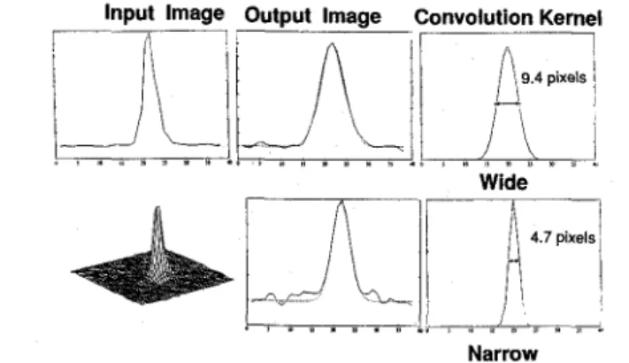
Our experiments suggest that a Gaussian with a width variable by a factor of 2 is adequate to smooth the noise in many simple images sampled at a resolution of 50 by 50 pixels.
We set about after these considerations to implement one analog integrated circuit capable of sampling an image at a resolution of 50 pixels on a side, smoothing it by a Gaussian in about 5 ps, and giving the user the flexibility of continuously varying the Gaussian width by a factor of 2:1. This speed of operation is orders of magni- tude faster than digital implementations of this convolu- tion function, which in addition to the requirements of image buffering also require the image to be circulated several times through a filter to obtain the property of variable width.
B. Computation in 2D Using Resistive Meshes
Resistor networks were used as analog computers in the past to solve complex boundary value problems in electromagnetic [12]–[15]. These were later replaced by numerical simulation on digital computers, primarily be- cause of the ease of programmability. Digital computa- tion, however, could neither surpass the low power dissi- pation nor the speed of analog computers, because when the latter solve complex 2D problems, the currents and voltages could attain their final values within a very short RC relaxation time. This high speed is the main attraction
of analog computation for 2D real-time signal processing, in that the number of calculations unlike digital computa- tion does not grow proportionally to the resolution, but more as the square root. The use of this concept for similar applications has also been noted elsewhere [16].
Unlike a resistive sheet subject to a potential difference between two edges, where the resulting lateral equipoten- tial contours solve electrostatic or magnetostatic field
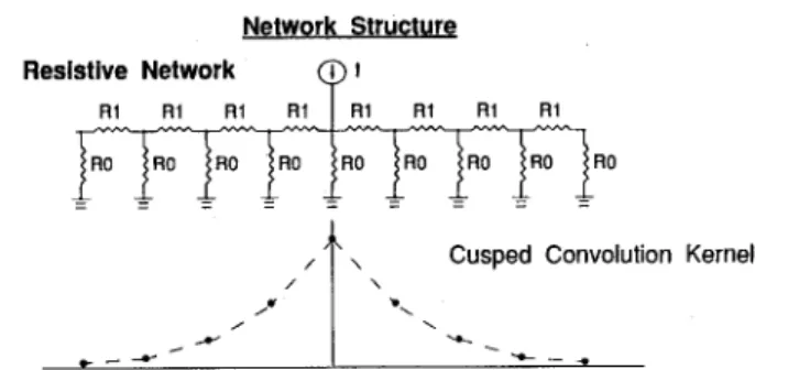
Network Structure Resistive Network
RI R1 R1 Ri
Cusped Convolution Kernel
Fig. 1. lD mesh with leakage resistors to ground, and its convolution kernel.
problems, the contours in a sheet which also has a contin- uous leakage to ground will decay in a characteristic fashion in response to a voltage applied at a single point.
The spatial rate of decay depends on the leakage conduc- tivity to ground relative to the lateral conductivity. This decay function may be thought of as the spatial impulse response of the leaky resistive sheet, or, equivalently, its convolution kernel; the potential contours in response to multiple-point stimuli will then be determined by linear superposition. Consider, for example, a one-dimensional discrete version of the leaky resistive sheet composed of a uniform linear mesh of resistors R 1 with resistors RO from every node to ground (Fig. 1). In response to a current excitation at one node, the resulting voltage dis-.
tribution on the mesh decays n nodes away from the excitation according to an exponential function exp(– nR ~/Ro) [16]. This convolution kernel differs from a Gaussian in two important ways: it has a slower decay at its tails, and the exponential on either side of the excita- tion meet at the center to produce a CUSP (Fig. 1). The discontinuity in derivative at this point would produce undesirable results when this function is applied to a noisy image and then followed by edge enhancement. The mesh must therefore be modified to produce a character- istic function which better resembles the flat-topped Gaussian at the point of excitation. Obtaining a practical realization of this mesh was one of the key contributions of our work.
C. An Active Resistive Mesh Implementing Gaussian Convolution
We first qualitatively examine why the resistive mesh in the previous example produces a cusped convolution ker- nel, and how it must be modified. An indirect procedure for synthesizing the desired network is then described, followed by methods to extend it to two dimensions.
The spatial derivative of voltage at a point in a resistive sheet or discrete mesh specifies the potential gradient or the electric field there. According to the point form of Ohm’s law, J = uE, a current injected at a point (assum- ing the point has nonzero extent, so that the current density there is not infinite) on a resistive sheet with leakage to ground will produce some nonzero electric field (E) there, and therefore a nonzero potential gradi- ent. A nonzero J may produce a zero E only if o –+%
740 IEEE JOURNAL OF SOLID-STATE CIRCUITS, VOL. 26,NO. 5, MAY 1991
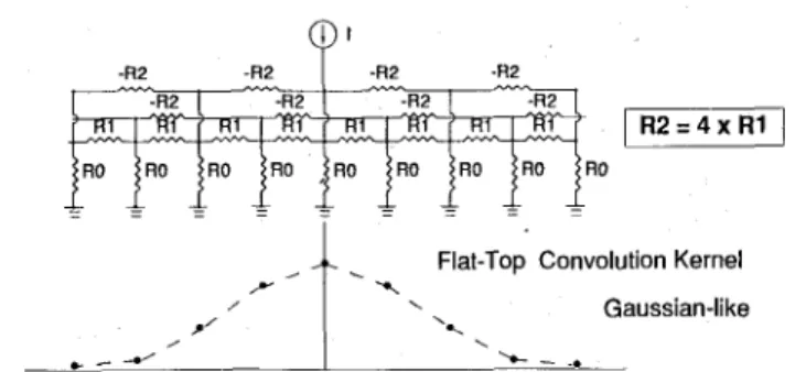
which implies that the sheet must appear perfectly con- ductive at the point of injection. If a negative resistance is introduced to locally neutralize the dissipation in the sheet, while maintaining the dissipation across the large scale, a convolution function may be obtained with a flat top and decaying tails. It is plausible to achieve this in a discrete resistive mesh by introducing negative resistors not between every node, because that would simply mod- ify the value of I?l, but between every other node, or perhaps even straddling several nodes. Investigating this numerically, we found that a mesh implementing a convo- lution of the desired shape could be obtained using nega- tive resistors of a certain value connecting nodes with their second nearest neighbors. We also came upon an alternative procedure to synthesizing the same mesh, based on the theoretical work relating to the optimal smoothing of images. This is now described.
Poggio et al. [9] have analyzed how to smooth samples
~, –@< j < ~, of a noisy function to best estimate the derivative if the noise were not present. They seek a fitting function U(x) with continuous first derivative which interpolates the sample points ~ with a least-mean-square difference, but with the constraint that the derivatives of U(x) are not allowed to fluctuate excessively to obtain the least noisy estimate of the actual derivatives of the sam- pled function. This is expressed as the problem of mini- mizing an energy functional E, defined as the mean square difference between the interpolating function and the samples, subject to a penalty on excessively large second derivatives. The strength of the penalty is con- trolled by a parameter A, called the regularization param- eter:
It is shown that the U(x) minimizing E in (1) is obtained by convolving ~. with an almost exactly Gaussian kernel, and the width of this kernel increases with A. We may use this result by exploiting a fundamental connection be- tween the minimum of an energy functional and the operating point of a circuit. It is known from circuit theory that Kirchhoff’s laws and the constituent relations of the components drive a network to a state of minimum energy dissipation, so it is reasonable to construct a network whose energy dissipation is described by (l). The network equations may be obtained directly by setting the derivative of the right-hand side of (1) to zero.
Using a discrete estimate of the second derivative in (l), we get
j j
where ~. = U(x = j). This is a quadratic form, and there- fore has a unique minimum where dE/dLJ = O for all j, so
o=2(~-~)+A;~(U+l+q.1-2q)2for all j.
11
(3)
-R2 -R2 -R2 .R2
Fig. 2. ID mesh with negative resistors between second nearest neigh- bors produces a cmvolution with a flat top.
Differentiating the terms in the sum and noting that d~./dL$ = O if i #j,
o=(q–y)+A(6q -4(q.l+q+l) +(q-2+q+2)).
(4)
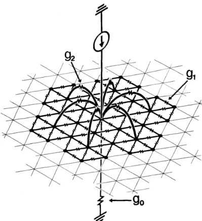
This describes the node equations of a one-dimensional mesh [17] consisting of positive resistors (1? ~) connecting nearest-neighbor nodes (i.e., j – 1, j and j, j + 1), negative
resistors ( – R2 = – 4R1) connecting second nearest
neighbors, and resistors R. = AR ~ to ground from every node, which are the leakage resistors described previously in the qualitative model (Fig. 2). The ~. correspond to voltage excitations in series with the leakage resistors.
The network will produce as an array of node voltages (1+) the convolution of the array of excitation voltages (~) with a Gaussian kernel whose width is controlled by A. If {~} were a set of photovoltages consisting of samples along a scan line through an image, the output set of voltages produced by the network would be the smoothed scan line.
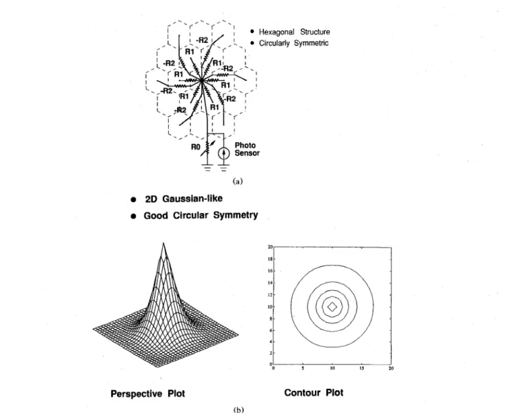
The desired smoothing in an image, however, must take place across two dimensions. To obtain this, samples of a 2D image as a matrix of photovoltages should drive a two-dimensional mesh to obtain the desired result. The one-dimensional prototype of a Gaussian convolution mesh must then be extended to implement the kernel with circular symmetry in two dimensions. Noting, for instance, that a two-dimensional Gaussian function G(x, y) is separable, that is, G(x, y) = G(x). G(y), the desired 2D convolution may be obtained by driving an array of lD meshes parallel to the y axis with the matrix of sampled photovoltages, and an identical array of lD meshes along the x axis with the matrix of buffered outputs from the first array. This is not very efficient in hardware, because each mesh must have independent active circuits to produce the negative resistances, and an intermesh buffer must be used at every node.
Another possible implementation on a 2D rectangular grid is to connect every node to its four nearest neighbors oriented 9(P apart with resistors RI, and the four second nearest neighbors at the same orientations with resistors – R2. The simulated spatial impulse response of this network decayed more rapidly along the diagonals than axially, producing an unacceptably large deviation from
KOBAYASHI et al.: ACTIVE RESISTOR NETWORK FOR GAUSSIAN FILTERING OF IMAGES 741
,., ., .
r ‘r’ ‘r’ ‘1
@ i.,.,: / ‘\, !
Ro d Photo
+ Sensor
— =
(a)
● 2D Gaussian-like
● Good Ch’cular Symmetry
● Hexagonal Structure
● Circularly Symmetric
‘1
20 18 16 14 12 10
Q
o
0
8 6 4 2 00
5 10 M 20
Perspective Plot Contour Plot
(b)
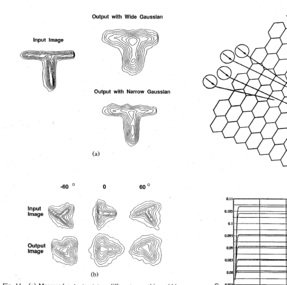
Fig. 3. (a) Extension of the mesh to 2D on a hexagonal grid produces (b) the best circular symmetry in the convolution kernel.
circular symmetry. A better circular symmetry was ob- tained by adding similar positive and negative resistive connections along the four diagonal directions, but weighted four times larger in magnitude. It became evi- dent that a large number of components would be re- quired to contrive circular symmetry on a rectangular grid, but not so on a hexagonal grid which inherently possesses a circular symmetry. The image must also be sampled on a hexagonal grid for compatibility with the mesh, “which now consists of equal resistive connections 6@ apart in orientation to nearest and second nearest neighbors. A hexagonal grid affords the greatest spatial sampling efficiency in the sense that the least photorecep- tor sites will attain a desired coverage of the image [181, and the fewest network elements will yield the desired circular symmetry (Fig. 3(a)). The latter was verified in the simulated convolution kernel of this 2D network (Fig.
3(b)).
We required the kernel width to be variable by a factor of 2 under user control. That the convolution width depends on the ratio RO /R1 was known from the synthe- sis procedure, but the strength of this dependence was
not, Simulations of the network showed a weak depen- dence (Fig. 4)
()
1/4Convolution width a ~ .
1
(5)
It was simplest in terms of implementation to keep RI and Rz fixed to preserve the Gaussian shape, and make RO alone variable by 16:1 to obtain the desired 2:1 variation in smoothing width.
Several aspects of this design procedure and simulated results invite analysis. Is there a systematic way to gener- alize a lD mesh prototype with circular symmetry to 2D?
Is the characteristic function of this combination of posi- tive and negative resistors stable in space (i.e., does it decay rather than oscillate indefinitely)? Stable in time?
Can the network be generalized to other convolution functions? What is the analytical relation between the width of the convolution function and the network ele- ments? We have answered some of these questions else- where [19].
742 IEEE JOURNAL OF SOLID-STATE CIRCUITS, VOL. 26, NO. 5> MAY 1991
Lambda
Fig. 4. The width of the convolution kernel increases as the l/4th power of the grounded resistor.
III. CIRCUIT DESIGN
The practicality of implementing this signal processing technique depends greatly on whether it is realizable on a standard (digital) CMOS IC process. We discuss now the circuit design of the required components, including the photosensors, and the special considerations for layout of this highly interconnected 2D network as a monolithic integrated circuit.
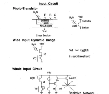
Inuut Circuit Photo-Transistor
Light
Light Vdd
( 3, collector N Substrate
~ Emitter
Vck Cross Section
Wide Input Dynamic Range
Light Vdd x
$
Vd M Iog(ld) Id
Vd in subthreshold
Whole Input Circuit
Vdd
Fig. 5. The vertical bipolar transistor in a CMOS well produces loga- rithmic compression at the gate voltage by a MOSFET in subthreshold.
A transconductance buffer drives the network.
Vin Vin Vin
!
Vc, /RO
——
ki+
t Ic — IIcA. Logarithmic Photoreceptor
An image focused on the chip surface maybe sampled by a matrix of photoreceptors, one at every node of the network. The intensity across a simple image may vary by two to three orders of magnitude in a Iaboratoty environ- ment, more in natural backgrounds, so a linear photore- ceptor, which converts the intensity to a proportional voltage or current, would drive the active circuits in the network into saturation. A logarithmic photoreceptor is
II = K[(VC -Vt) Vin -~Vin2]
(in triode region) 12= K[(Vc+Vin -Vt)Virr-~Vin2]
1=11+12= 2K[Vc-Vt]Vin
Fig. 6. The linearized variable resistor, with implementation of gate bias.
therefore required, and as studies on image Processing level-shift PMOS driving a resistively degenerated have shown, perfectly adequate for the task on hand [3]. NMOSFET, which appears to the photoreceptor as a photosensing is most economically obtained using the voltage-controlled current source (Fig. 5).
parasitic vertical bipolar in a CMOS well as a phototran- sistor, whose collector current becomes proportional to the light intensity incident on the collector junction along the well bounda~. This may be compressed into a loga- rithmic voltage by a diode-connected MOSFET biased in the subthreshold region by the small photocurrent density produced under room lighting conditions. A compact logarithmic photoreceptor is in this way obtained with a two-transistor circuit [20], [21] (Fig. 5).
Although the stimulus to the prototype network in the discussion above was a voltage source in series with the variable resistor RO, the circuits for the photosensor out- put and RO (described below) are naturally grounded on one end, so the Norton transformation must be invoked to convert the stimulus into a parallel combination of a grounded current source and a shunt resistor. A transcon- ductance photoreceptor buffer was used, consisting a
B. Variable Resistor
The width of the convolution kernel is set by a resistor RO, whose value should ideally be continuously variable under user control. A single MOSFET operating in triode region used as a variable resistor would introduce an undesirable parabolic nonlinearity in the 1 – V character- istics. Two MOSFET’S in parallel obeying the simplified square law equations, however, can exactly cancel each other’s parabolic nonlinearity in the triode region of oper- ation if their gate biases are applied in a particular way, and the resulting linearized resistance is controlled by the bias. We used this as the variable resistor (Fig. 6). The floating-gate bias voltages were obtained as the V& of source-follower FET’s carrying a control current.
KOBAYASHI et al.: ACTIVE RESISTOR NETWORK FOR GAUSSIAN FILTERING OF IMAGES 743
Vaa baa
J
(nodeV.avA)5’ I’L
(node B)l=av/R2 ‘2 (node C) t (nose D]J ‘i’”’”” +!? ) r
Vss Vss
(node A) - R2 (node D]
V.clv v
l=OV/R2 (a)
Vda
(b)
Fig. 7. (a) An NIC inverts the polarity of a resistor. (b) One NIC serves all resistors converging on a node.
The mean network voltage at a given level of ,photosen- sor illumination will change with the convolution width:
for example, when the convolution width is decreased by making all RO large, the mean voltage will also increase because the buffered photocurrents will flow into larger resistors. This will impose the unnecessary demand of a large common-mode range of operation in active circuits such as RO. We used a scheme to normalize the network inputs by slaving the buffer transconductance of the loga- rithmic photoreceptor proportionally to RO, so as to maintain a constant mean network voltage at all illumina- tions.
C. Network Resistors
The 5-kfl resistors for the nearest-neighbor internode connections in the network were implemented using p-well diffusions. A Gaussian convolution kernel would be ob- tained in spite of tolerances in the p-well resistivity as long as the relative magnitude of the positive and nega- tive resistors remains 1:4. To make this ratio on the chip depend only on geometry, both RI and Rz were imple- mented in the same material, p-well diffusion, and a negative impedance converter (NIC) was attached to R2 to invert its polarity.
Our NIC implementation (Fig. 7) consists of the combi- nation of a voltage follower and current inverter. The op-amp-based followers at each end of Rz impose across it the potential difference at their inputs, and the result- ing current flow, forced through the Class-B type output
stages, is sourced from or sunk into the positive or nega- tive power supply. Current mirrors in series then apply the same current at the input leads of the followers, inverting the sense of current flow as perceived at the network nodes. A negative resistance – R2 is presented to the network.
Six negative resistors converge on every node in this hexagonal mesh. Six different NIC’S are, however, not required at each node; instead, a single NIC placed at the node after the confluence of the resistors will simultane- ously make them all negative (Fig. 7(b)). The dc gain in a simple five-FET op amp was large enough to obtain accurate inversion of the resistor 1– V characteristics and eliminate the crossover nonlinearity in the Class-B stage.
The NIC at every node thus contained only 11 FET’s.
D. Layout Considerations
A key concern in the implementation of this network as an IC is whether the usual two layers of metal and one of polysilicon can implement the starlike fan-out of intercon- nections emanating from every node. We proved to our- selves at the outset of this work that this was possible. A hexagonal grid was obtained by horizontally staggering successive rows of cells, and their interconnections imple- mented on a Manhattan geometry (Fig. 8(a)). All three available layers of interconnect were used to create abut- table cells. The power, ground, control, and output rails ran parallel to these rows from edge to edge of the chip.
A unit celI, including its portion of interconnect, mea- sured 170 X 200 ~m in 2-pm CMOS (Fig. 8(b)). The area of the photoreceptor collector–base junction, the blank rectangle in the cell layout at the lower left, measured 56X 24 pm. No wires were allowed to traverse the photo- sensor because metal would absorb the incident light.
Parasitic photocurrents generated in the source/drain junctions of other active circuits would have negligible
effect on the voltages at the low-impedance nodes there.
We observe finally that the active circuits occupied only 57% of the cell area, a measure of the toll exacted by the richness of interconnect in this circuit.
E. Output Means
This convolution network accepts a 2D input in the form of an incident image, does 2D signal processing across the resistive mesh, but on a standard IC is re- stricted to ID output at the pins along the periphe~. The output therefore must be read at the pins (Fig. 9) by accessing one row of nodes at a time, and, at least in this implementation, becomes the bottleneck to the through- put rate. Addressable MOS switches were used to con- nect every node to output lines, and on-chip vertical bipolar transistors connected as emitter followers served as analog buffers at the pads. The speed of signal process- ing was determined by the relaxation time of this un- clocked network, but a clock was introduced at the output to scan out the rows. To relieve this bottleneck, one can

![Fig. 3. Spatial impulse responses with n = 61, rn = 2 , ]/go = 200 kR, l / g i = 5 kR, U 3 1 = 10 PA, u k = 0 for IC # 31](https://thumb-ap.123doks.com/thumbv2/123deta/7124948.2346491/33.928.474.818.88.851/fig-spatial-impulse-responses-rn-kr-pa-ic.webp)
