SUMMARY We have developed the world’s largest 16.7-inch hybrid in-cell touch panel. To realize the large sized in-cell touch panel, we ap- plied a vertical Vcom system and low resistance sensor, which are JDI’s original technologies. For glove touch function, we applied mutual bun- dled driving, which increases the signal intensity higher. The panel also has a low surface reflection, curved-shaped, and non-rectangular charac- teristics, which are particular requirements in the automotive market. The over 15-inch hybrid in-cell touch panel adheres to automotive quality re- quirements. We have also developed a force touch panel, which is a new human machine interface (HMI) based on a hybrid in-cell touch panel in automotive display. This study reports on the effect of the improvements on the in-plane variation of force touch and the value change of the force signal under different environment conditions. We also a introduce force touch implemented prototype.
key words: in-cell touch panel, low-temperature polysilicon TFT
1. Introduction
The increasing demand of autonomous driving in recent au- tomotive markets has led to the improvement in car inte- rior design. The importance of the touch panel as a hu- man machine interface (HMI) is increasing; in particular, the demand for large size, curved-shaped, and non-rectangular shaped displays is increasing.
This study proposes to replace amorphous silicon (a- Si) TFT panels with low-temperature polysilicon (LTPS) TFT panels that offer high functionality. LTPS TFT has a high mobility, resulting in high resolution owing to the re- duced TFT size and a built-in circuit in a panel that can re- duce the number of gate driver and source driver ICs[1].
2. In-Cell Capacitive Touch Panel Method
LTPS TFT must have an in-built circuit for integrating touch functions in the panel. The development of touch panel in-cell technology has been accelerated with the increas- ing use of LTPS TFT. In-cell capacitive touch panels are roughly classified into hybrid in-cell and full in-cell touch panels[2]–[4].
Figure 1 shows a comparison of hybrid in-cell touch panels and full in-cell touch panels. Hybrid in-cell touch panels use a mutual sensing method. This panel comprises a receiver sensor (Rx) on the back side of the color filter
Manuscript received March 18, 2019.
Manuscript revised June 5, 2019.
†The authors are with Japan Display Inc., Ebina-shi, 243–0432 Japan.
a) E-mail: [email protected] DOI: 10.1587/transele.2019DII0005
Fig. 1 Type of in-cell capacitive touch method
glass and a driving transmitter (Tx) with a Vcom (com- mon electrode for display drive) layer on the TFT glass. A self-sensing method can also be realized using Tx and Rx electrodes as sensor electrodes. Hybrid in-cell touch pan- els can detect a floating conductor via mutual sensing and self-sensing. Therefore, it is possible to track a finger on the panel surface where water is attached.
In contrast, full in-cell touch panels only use the self- sensing method. Full in-cell touch panels are cost-effective because Rx electrodes are configured in the Vcom layer, which eliminates the needs for the flexible printed circuit mounted on the back side of the color filter glass.
In full in-cell touch panels, Rx electrodes located in a panel must be directly connected to the in-cell touch dis- play drive IC. Therefore, the number of Rx electrodes con- siderably increases with increasing screen size. Therefore, hybrid in-cell touch panel is more advantageous than full in-cell touch panel when considering application to larger panels.
3. New Technologies and Results
3.1 16.7-inch Hybrid In-Cell Touch Panel Development We have promoted the development of conventional hybrid in-cell touch panels in the mobile phone market[5], [6].
In the development of the 16.7-inch hybrid in-cell touch panel, we have applied advanced hybrid in-cell technolo- gies, which involve vertical Vcom systems and low resis- tance materials on the top and bottom segments of the source line, as shown in Fig. 2.
Copyright c2019 The Institute of Electronics, Information and Communication Engineers
Fig. 2 Applied technologies to 16.7-inch hybrid in-cell touch panel
Fig. 3 Comparison of surface reflection between external TP module and hybrid in-cell
The vertical Vcom system divides the Vcom (Tx) in a parallel direction to the source line. Divided common elec- trodes function as transmitter electrodes (Tx). The parasitic capacitance between the Vcom and the source line can be reduced by modulating the source line with the Vcom volt- age. As a result, the RC constant of Tx electrodes can be reduced. The ITO (indium tin oxide) layer to protect the panel elements from being destroyed by the ESD (Electro- Static Discharge) is conventionally used as Rx electrodes.
We have replaced the ITO with a low resistance material.
Application of the low resistance material has the effect of lowering sensor resistance.
Furthermore, there is also the effect of reducing reflec- tion on the back side of the color filter glass, more so than the external touch module and conventional hybrid in-cell touch panels, as shown in Fig. 3.
In order to further shorten the driving period, we di- vided the signal lines into top and bottom segments. By us- ing this method, the upper and lower sides of the panel are simultaneously written. Therefore, it is possible to shorten the display drive time by half.
Fig. 4 Estimation of total driving period
Figure 4 shows an estimation of the total time of touch and display driving period. In prior art of our hybrid in- cell touch panel, the total period was estimated as 114 ms.
Here the touch driving period could be reduced by 9/10, by applying the low resistance material as Rx electors and the vertical Vcom system. Display driving period could be re- duced by half by applying the top and bottom segmentation of the signal line system. As a result, a total period of 16 ms was accomplished.
Mutual bundled driving, which is one of the hybrid in-cell evolution technologies previously developed[5],[6], is also applied to the 16.7-inch hybrid in-cell touch panel.
Mutual bundled driving is important to support stylus pens;
however, there is not much demand for this in the automo- tive market. Meanwhile, there is a great demand for glove support and using plastic materials for the cover lens.
In the case of glove touch, the distance between fin- gers and Rx electrodes becomes larger than in surface touch where the panel surface is touched by a finger. Plastic ma- terial typically has a lower dielectric constant compared to glass material. Therefore, in order to support glove touch with a plastic cover lens, the signal intensity needs to be strengthened. Figure 5 shows the principle of mutual bun- dled driving. Mutual bundled driving makes the Tx elec- trode width half of the conventional Tx width. Three narrow Tx electrodes are bundled and driven at the same time. The bundling of Tx electrodes is shifted by two, and Tx elec- trodes are driven in the same way. The signal intensity be- comes 1.5 times higher and the sensor pitch resolution is the same as the surface driving by using mutual bundled driving.
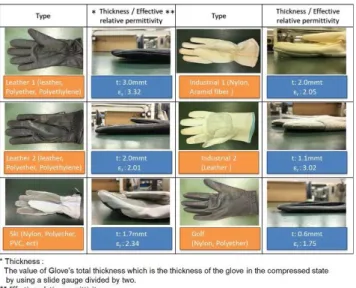
We evaluated glove touch performance by using the bundled drive described above. The glove types used for the evaluation are shown in Fig. 6. Table 1 shows the eval- uation result when the cover thickness and the cover ma- terial (glass or plastic) are changed. In the case of glass, all types of glove can be detected with 3 mm cover thick- ness. In the case of 2 mm plastic thickness, which is made of polycarbonate, all types of gloves can be detected when the Tx amplitude voltage is 5.5 V. In the case of 3 mm plas-
Fig. 5 Principle of Mutual bundled driving
Fig. 6 Glove type
tic thickness, all types of gloves can be detected when the Tx amplitude voltage is 7.5 V.
One of the negative effects of increasing glove detec- tion is the detection of non-touch finger above the panel, called hover detection. The signals of gloves and hovers correlate with the ratio of the effective relative permittivity of the glove, the thickness of the glove, and the relative per- mittivity of the airgap (εr =1). Among the gloves used for evaluation, Leather2 had the lowest signal strength. When hover’s airgap was 1.2 mm, the signal strength of the hover was equal to that of Leather2. That is, if a finger is placed above the panel and the airgap is less than 1.2 mm, there is a risk of hover detection.
Table 2 shows the specifications of the prototype. Fig- ure 7 shows a prototype of the 16.7-inch hybrid in-cell touch
Table 2 Specification of prototype
Fig. 7 A prototype of the 16.7-inch hybrid in-cell touch panel
panel. We also succeeded in realizing a curved-shaped panel with curvature of 800 mm and a hexagonal type panel. Fur- thermore, we also developed an over 15-inch hybrid in-cell touch panel and it passed the in-vehicle quality require- ments.
3.2 Force Touch Panel Development
Until now, we have been developing an improvement to the touch performance of an in-cell touch panel. In addition, in
Fig. 8 In-cell touch panel technology evolution of JDI
the future, we are going to develop a new HMI, such as force touch technology, which detects pressure and incorporates proximity technology, which detects hands approaching or gesturing in the air, and hover technology, which detects fin- ger coordinates in the air, as shown in Fig. 8. The assumed use-case situations are as follows:
• First step: the system is activated when a hand ap- proaches a few centimeters above the screen
• Second step: the system selects a rough menu and wakes up an application by gesture or finger coordi- nates above the screen
• Third step: the system selects a detailed menu by finger touch
• Final step: the system confirms the final selection by finger pressure
To realize the use-case written above, we are aiming to de- velop the total system technology by combining the tech- nologies of proximity, hover, and force touch. At this time, we will report on the development of force touch.
Figure 9 describes the operation principle of force touch. The system configuration is based on the conven- tional hybrid in-cell touch panel configuration. Rx elec- trodes for force touch are added to the bottom of the back- light materials. When a pressure is applied to the glass surface, the glass bends and the air gap changes. Force touch uses the capacitance change due to this air gap change.
Since the amount of deflection of the glass, i.e., the amount of air gap change, depends on the pressure, it is possible to calculate the pressure from the capacity change.
Both surface touch and force touch use the mutual sens- ing method. In the surface touch case, the Vcom is used as a Tx electrode and the layer on the back side of the color filter is used as Rx. On the other hand, force touch uses the same Tx electrodes and a newly added layers on the back- light materials as Rx electrodes for force touch. Our force touch driving method has two benefits. The first is that addi- tional time is not required because it is possible to detect sur- face touch and force touch at the same time. The second is
Fig. 9 Operation principle of force touch.
Fig. 10 Procedure of force value compensation
that the signals of a finger and force touch can be separated because the capacitance detection locations of surface touch and force touch are different. In the case of self-sensing, such as in full in-cell, the signals of a finger and force touch are merged. Therefore, it is necessary to separate them.
This force touch detection method has an in-plane dis- persion of force signal. The amount of deflection (σ) de- pends on the distance between fulcrums (L) of the module, the strength of the press (W), and the elastic modulus of the module. Longer “L” and larger “W” make “σ” larger.
Therefore, even if the strength of the press is constant, the amount of deflection varies depending on the location of the panel. The center of the panel is easy to deflect, and the edge of the panel is harder to deflect.
Figure 10 illustrates a procedure to compensate the in- plane variation of force signal, where the force value is com- pensated from the force signal and finger position informa- tion. The Look Up Table is preliminarily made by the fol- lowing procedure: first, known weights are put on a panel with several positions, and second, the force signal for the known weight is correlated with the surface touch position.
Since the place where the weight is put can be known by the surface touch force value, it is possible to compensate ac- cording to the position of where a finger is pressed (Fig. 11).
Since there are several variation tolerances, such as cushion pasting tolerance and backlight frame thickness tol- erance, etc., in-plane compensation for each module is nec- essary.
We evaluated the force value variation with five sam- ples before compensation and after compensation.
Fig. 12 Evaluation conditions
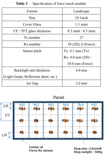
Table 3 shows specification of force touch module. We used these modules for evaluation. Evaluated positions are 18 points, as shown in Fig. 12. We used a 12 mm phi slug with 500g weight.
Figure 13 shows maximum force value variation before compensation and after compensation. The below procedure shows the calculation of maximum force value variation:
1. Calculate the standard deviation (σ) between five sam- ples at each position (18 points)
2. Calculate the average force value between five samples at each position (18 points)
3. Normalize 3σby the averaged force value at each po- sition (18points)
4. Select the maximum value from the outputs in the third procedure
Maximum in-plane variation after compensation de-
creased from 82% to 21%, which is about one–fourth of that before compensation.
We would like to add the effects of thicker cover glass and cover plastic as well. In the case of the automotive mar- ket, cover glass of 1 to 2 mm thickness and cover plastic of 2 to 3 mm thicknesses are generally used.
First, we estimated the impact of thicker glass. When the same stress is applied to the center of the panel of the force touch prototype, and the thickness of the cover glass is increased from 1.1 mmt to 2.0 mmt, the glass deflection is reduced to about 40%. The deflection of the glass correlates with the signal strength of the force touch linearly. There- fore, when the amount of deflection of the glass is reduced to about 40%, the signal strength of force touch is also re- duced to about 40%. The signal strength of force touch can be improved by applying a higher voltage or narrowing the airgap.
Second, we would like to comment on the impact of the cover plastic. The amount of deflection of the cover is determined by Young’s modulus and stress as expressed by the following equation:
ε= σ
E (1)
(ε: strainσ: stressE: Young’s modulus) The plastic cover made of polycarbonate has a sufficiently small Young’s modulus to the cover glass. Therefore, the signal strength of the plastic cover is more sensitive than the signal strength of the cover glass.
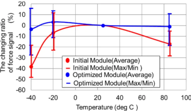
Further issues of force touch are reliability and tem- perature dependency. A module is composed of various materials such as cover glass, glue, polarizer, TFT glass, color filter glass, cushion, backlight unit, etc. The position, thickness, or elastic constant of these construction materials change due to temperature changes and aging. As a result, the force value deviates from the initial force signal. We evaluated the temperature dependence in the range of−40 deg C to 85 deg C. We have also evaluated the reliability at high temperature and high humidity (65 deg C, 93%) and high temperature (85 deg C) under the condition of operat- ing the panel.
The result of temperature dependence is shown in Fig. 14. The vertical axis shows the changing ratio of force value with respect to the force value at 25 deg C. In the ini-
Fig. 14 Temperature dependence test (−40 deg C to 85 deg C)
Fig. 15 Reliability test (after 1000hr w/operation)
tial module configuration, the force value decreases by 48%
at maximum. This behavior is observed at low temperatures.
The main factor is that the elastic constant of the construc- tion materials increases at low temperatures. By optimizing the construction materials of the module, the change ratio of force signal was improved up to 27%, at the maximum.
The reliability test result is shown in Fig. 15. The ver- tical axis shows the changing ratio of force value with re- spect to the force value before the reliability test. In the case of the initial module configuration, the force value in- creases by 64%, at the maximum, in the high temperature and high humidity condition (65 deg C, 93%) and by 102%, at the maximum, in the high temperature condition (85 deg C). In the reliability test condition, an irreversible structural change such as warpage occurs. By optimizing the construc- tion materials, the irreversible structural change hardly oc- curs and the rate of change of force value was improved up to 22%, at the maximum, in the high temperature and high humidity condition, and by 25%, at the maximum, in the high temperature condition.
4. Conclusion
We have succeeded in developing the world’s largest 16.7- inch hybrid in-cell touch panel as well as passing the au- tomotive quality requirements with the over 15-inch hybrid in-cell touch panel.
We also have developed force touch technology based on the 10.1-inch hybrid in-cell touch panel.
We have tried to improve the in-plane variation of force touch, the force value change due to temperature change, and the force value change due to the reliability test.
Maximum in-plane variation after compensation de- creased from 82% to 21%, which is about one–fourth of that before compensation.
We have also succeeded in suppressing the changing ratio of force signal in the temperature dependence and reli- ability test. The changing ratio of force signal was 27% with respect to the force signal at 25 degrees C, at the maximum, in the temperature dependence test and 25% with respect to the force signal before the reliability test, at the maximum, in the reliability test.
Acknowledgments
I would like to express my heartfelt gratitude to Mr. Kazu- taka Nagaoka and Mr. Yoshiharu Nakajima for giving accu- rate suggestions based on their expertise. I am also grateful to Mr. Toru Murakami and Mr. Satoshi Morita for their ad- vices based on their experiences. I would like to thank to Mr. Nobuo Tsubokura and Mr. Takuya Nishimoto for sup- porting sample preparation and evaluation.
References
[1] N. Takada et al., “A new low power driving method for high resolution mobile IPS LCDs,” 11.3, SID 2008.
[2] C. Kim, D.S. Lee, J.H. Kim, H.B. Kim, S.R. Shin, J.H. Jung, I.H.
Song, C.S. Jang, K.S. Kwon, S.H. Kim, G.T. Kim, J.H. Yoon, B.-Y.
Lee, B.K. Kim, and I.-B. Kang, “Advanced in-cell touch technol- ogy for large sized liquid crystal displays,” SID Symposium Digest of Technical Papers, vol.46, no.1, pp.895–898, 2015.
[3] K. Noguchi et al., “Novel in-cell capacitive touch panel technology in a wide viewing angle IPS-mode display,” 11.3, EuroDisplay 2011.
[4] K. Noguchi et al., “Newly developed in-cell capacitive touch panel technology in a wide viewing angle IPS-mode display,” INP3/AMD6- 1, IDW 2012.
[5] D. Ito et al., “Newly Developed 5.5inch WQHD Display with Hybrid In-cell Capacitive Touch Technology,” INP2-4, IDW 2015.
[6] Y. Teranishi, K. Noguchi, H. Mizuhashi, K. Ishizaki, H. Kurasawa, and Y. Nakajima, “New In-cell Capacitive Touch Panel Technology with Low Resistance Material Sensor and New Driving Method for Narrow Dead Band Display,” SID Symposium Digest of Technical Papers, vol.47, no.1, pp.502–505, 2016.
Naoki Takada received the B.S. and M.S.
degrees from Tokyo Institute of Technology in 2000 and 2002, respectively. During 2002–
2014, he stayed in Hitachi Ltd. He is now with Japan Display Inc.
the M.Eng. degrees in Tottori University in 1979 and 1981, respectively. During 1981–2003, he stayed in Tottori Sanyo Electric Co., Ltd. Dur- ing 2003–2004 in Sanyo Electric Co., Ltd. Dur- ing 2004–2006 in Sanyo Epson Imaging De- vices Corporation. During 2006–2010 in Epson Imaging Devices Corporation. During 2010–
2012 in Sony Mobile Display Corporation. He is now with Japan Display Inc.
Yuto Kakinoki received the B.Eng. and M.Eng. degrees in Doshisha University in 2015 and 2017, respectively. He is now with Japan Display Inc.
Takayuki Nakanishi received the B.E.
and M.E. degrees in Electrical Engineering from The University of Electro-Communications. He joined CASIO Computer Co., Ltd. in 1995, SONY Corp. in 2003, and Japan Display Inc.
in 2012. His research fields include display cir- cuits and system designs for TFT-LCDs.
Naoshi Goto received the B.S. and M.S.
degrees in Engineering from The University of Electro-Communications in 1991 and 1993, re- spectively. During 1993–2012, he stayed in Sony Corporation. He is now with Japan Dis- play. Inc.