SUMMARY We describe an In-Cell Projected Capacitive Touch Panel in a display using IGZO TFT technology. The prototype demonstrates high signal-to-noise ratio (SNR) and pen input operation. The possibility of en- larging the display size beyond current limits makes this a highly promising approach for In-Cell Capacitive touch panels.
key words:in-cell touch panel, pen input, high SNR, projected capacitance
1. Introduction
In recent years, the mainstream touch panel technology in the mobile device market has become projected mutual ca- pacitance technology. In the future, the touch panel market is predicted to expand for smartphones, tablet PCs, and PC monitors for Windows 8 [1]. In order to reduce cost, an out- cell type touch panel technology, known as “One Glass So- lution”, in which the touch sensor is located directly under the cover glass, is being rapidly developed.
The desire for a thinner module, lower weight, reduced overall manufacturing cost and a changing business model [1] is driving a trend towards integration of the touch panel into the LCD. This approach is known as “In-cell” type touch panels, as shown in Fig. 1. However, the In-cell type has essentially lower SNR than the out-cell type because the finger is further away from the touch sensor and the touch sensor is located nearer the LCD which is a major noise source. Therefore, there are many technical challenges for the In-cell touch panel LCD.
To overcome these challenges, we have previously demonstrated various In-cell type touch panel technologies including a liquid crystal capacitance sensor [2] and optical sensors [3]–[5].
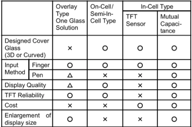
In recent years In-cell projected capacitance technolo- gies have been previously reported by TMD [6] and Sony [7]. Table 1 shows a category of capacitive touch panel technologies. First, the overlay type “One Glass Solution”
(OGS) technology cannot be applied to a designed cover glass (e.g. 3D or Curved or Rounded). Further, OGS tech- nology has higher cost than other in-cell touch panel tech- nologies because a custom-designed sensor array is needed in every product model. Next, for the On-cell type and the semi-In-cell type (i.e. with a patterned sensor on top of the counter glass underneath the polarizer) the overall manufac-
Manuscript received March 11, 2013.
Manuscript revised June 10, 2013.
†The authors are with Sharp Corporation, Tenri-shi, 632-8567 Japan.
a) E-mail: [email protected] DOI: 10.1587/transele.E96.C.1384
Fig. 1 Trend of touch panel structure.
Table 1 Comparison of capacitive touch panel technologies.
turing cost is higher than other in-cell technologies, because a patterning process on both sides of counter glass and an extra FPC is required. It is also not suitable for large size panels, because the One Drop Fill method used in conven- tional manufacturing equipment cannot be applied to this type. Finally, the In-Cell type (TFT sensor type) has low SNR, because of parasitic capacitance, and is of limited use in large size displays due to reliability issues of amorphous Si TFTs (e.g. Vt shift).
In this paper, we present an In-Cell Projected Capac- itive Touch Panel in a display using IGZO TFT technol- ogy. The prototype demonstrates high signal-to-noise ra- tio (SNR) and pen input operation. Our simple proposed structure for the In-cell touch panel can also be applied to a backplane with either LTPS TFTs or amorphous Si TFTs technology.
2. Key Issues for In-Cell Capacitive Touch Panel
2.1 RC Delay
This section shows the first key issue, RC delay. A con- ventional LCD consists of an array of some electrodes, for example, common ITO, pixel ITO, gate line, and data line.
Copyright c2013 The Institute of Electronics, Information and Communication Engineers
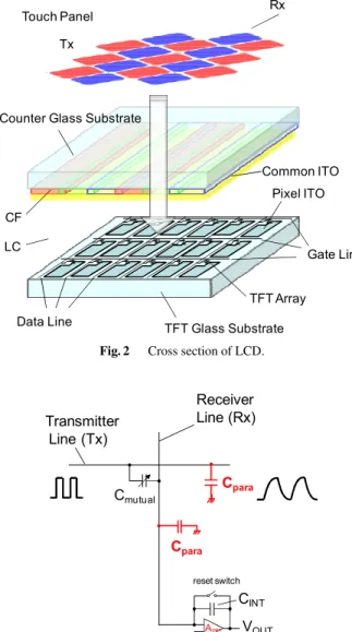
Fig. 2 Cross section of LCD.
Fig. 3 Equivalent circuit of touch panel sensor.
The sensor layer of the touch panel is inserted between the counter glass substrate and the TFT glass substrate, as shown in Fig. 2. Since the distance between sensor elec- trodes and each electrode of the LCD is reduced, the capac- itive load increases drastically. The distance is about a few micro-meter order.
Figure 3 shows the equivalent circuit of the touch panel sensor. The horizontal line is a transmitter electrode and the vertical line is a receiver electrode. The capacitance of the intersection of two lines is the mutual capacitance between sensor electrodes, and the receiver electrode is connected to an integrator. The symbol “Again” shows the open-loop gain of the integrator amplifier. In general, the driving frequency of the transmitter line is approximately 100 kHz to 200 kHz in smartphones, tablet PCs and the prototype.
In case of the in-cell touch panel, the distributed par- asitic capacitances of the transmitter and receiver lines are included in the equivalent circuit as indicated.
In the case of the transmitter line, increasing the dis- tributed capacitive load causes a slow response time due to
Fig. 4 Measurement of LCD noise.
the RC delay. The C value of the Tx electrode in the pro- totype is approximately 1000 pF. This leads to a reduction in the number of samples that made be made for each ca- pacitance measurement. The noise level is inversely propor- tional to the square root of the number of the samples as shown in the Eq. (1). As a result, the noise level increases.
Noise∝ 1 Nsample
(1) On the other hand, in the receiver line connected to an integrator, the increasing distributed capacitive load causes a reduction of signal level. The integrator increases the effect of the distributed capacitance by a factor of one over the gain A, as shown in Eq. (2). And, as the distributed capacitive load increases, the signal efficiency decreases.
Signal efficiency= CINT
CINT+CparaciticAgain (2)
In this way, the increasing capacitive load causes worse touch panel performance (SNR).
2.2 LCD Noise
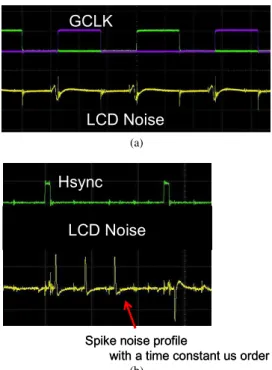
This section describes a second key issue, LCD noise. As mentioned above, the In-cell type touch panel has essentially lower SNR than the out-cell type because the touch sensor is located nearer the LCD which is a major noise source. We measured the noise waveforms from the display surface, as shown in Fig. 4.
In the case of the prototype LCD with IGZO TFTs, the noise is generated at the rising edge and the falling edge of GCLK, as shown in Fig. 5(a).
In the case of other standard LCDs with LTPS TFTs, the noise is generated when the gate of the Source Shared Driver is ON, as shown in Fig. 5(b).
The LCD noise is generated when the voltage of the GCLK or data line is changed and exhibits a spike noise profile with a time constant of theμs order. As a result, the noise radiates from the LCD. The integration of the touch panel into the LCD causes the increasing noise level in the sensor. Therefore, the LCD noise is a second critical issue.
(b)
Fig. 5 (a) LCD noise waveform of prototype LCD. (b) LCD noise waveform of standard LCD.
Fig. 6 Cross section of prototype LCD.
3. In-Cell Capacitive Touch Panel
3.1 Display Area Structure
Figure 6 shows a cross section view of the In-cell touch panel LCD. The panel is fabricated with IGZO TFT tech- nology. The sensor layer is formed between the counter substrate and common ITO layer.
3.2 Sensor Pattern
Figure 7(a) shows the sensor pattern and structure. The touch panel sensor layers are formed by ITO electrodes and a metal Black Matrix (BM). The sensor ITO and metal BM
(a)
(b)
Fig. 7 (a) Sensor electrode pattern. (b) Sensor metal black matrix layer.
are connected with via holes in every pixel. The metal BM is patterned together with the ITO by a fine pitch LCD pro- cess — as shown in Fig. 7(a) and Fig. 7(b).
As a result, the X sensor electrodes are connected by the ITO layer, and the Y sensor electrodes are connected by the metal BM. The metal BM enables drastically lower resistance than a conventional ITO sensor.
The In-cell touch panel enables simple structure only adding one sensor layer (ITO) by using Metal BM. As a result, this structure enables the sensor electrode to have a drastically lower resistance than conventional out-cell types.
The R value of the Tx electrode in the prototype is less 100Ω. Further, this effect is achieved without a visible sen- sor pattern or Moire pattern, without decreasing the LCD aperture ratio and without increasing cost.
3.3 Advantage of Proposed Structure
Figure 8 demonstrates the advantage of proposed sensor structure. First, Fig. 8(a) shows the resistance of the sen- sor electrode. The resistance of the sensor electrode of the proposed in-cell touch panel is about one hundred times smaller than the conventional ITO sensor electrode. Fig-
Fig. 8 Advantage of proposed structure.
ure 8(b) shows the RC delay of the Tx electrode. The RC delay of the proposed in-cell touch panel is the same as the conventional out-cell type sensor electrode.
In order to prevent decreasing the signal efficiency, the open-loop gain A of the integrator amplifier is fixed above 100 dB.
The advantage of proposed sensor structure is summa- rized as follows. This structure enables the sensor electrode to have a drastically lower resistance than conventional out- cell types without a visible sensor pattern or Moire pattern, without decreasing the aperture ratio and without increas- ing cost. As a result, The RC delay of the proposed in-cell touch panel is same as the conventional out-cell type sensor electrode.
By using a metal black matrix, the In-cell touch panel has a simple structure and process with only one additional ITO layer.
Therefore, first key issue can be solved by using pro- posed structure.
4. Timing Diagram for Sensing Operation
We now describe two sensing schemes of the In-cell touch panel operation.
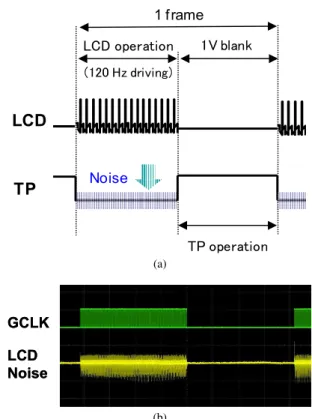
4.1 Sensing Operation in V-blank Period
Figure 9(a) shows the timing chart of the display operation and touch panel operation. As shown, the In-cell touch panel sensing operation is performed in a vertical blanking (V- blank) period of an LCD operating at a frame rate of 120 Hz (“120 Hz driving”). As shown in Fig. 9(b), the noise from the LCD is not observed in the V-blank period of the LCD.
Therefore, this touch panel operation method can eliminate the effect of the driving noise from the LCD. The common electrode functions as a noise shield from the LCD. This sensing scheme in the V-blank period can also be combined with a low frame frequency technology made possible by using IGZO TFTs [8]. This approach enables higher SNR of the touch panel, lower power consumption of the display and enlargement of the display size.
4.2 Sensing Operation in 1H Period
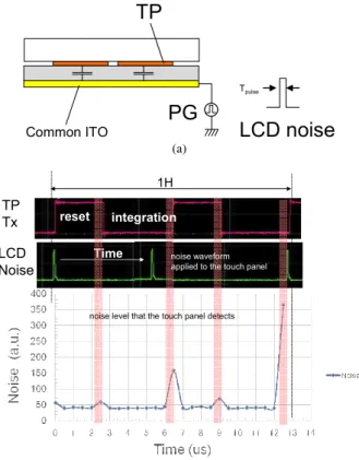
Figure 10 shows the noise effect in a touch panel. As shown
(a)
(b)
Fig. 9 (a) Timing of display and touch panel. (b) LCD noise in V-blank period.
in Fig. 10(a), in order to investigate the influence of the noise received by the touch panel, pulses of fixed voltage were applied to the touch panel. These noise pulses are used to approximate the LCD noise waveform and the time at which a noise pulse is applied is varied systematically with respect to the touch panel control signals. The upper figure of Fig. 10(b) shows the voltage waveform of the transmit electrode, Tx, of the touch panel, and the middle figure of Fig. 10(b) shows the noise waveform applied to the touch panel. The lower figure of Fig. 10(b) shows the noise level that is detected by the touch panel. The noise pulse is ap- plied at various times during the reset period and the sam- pling period.
As a result, it is seen that the noise level detected by the touch panel increases drastically when the noise pulse is applied at the end of integration. Therefore, by separating the end of the reset period and the sampling period from the spike noise, high SNR of the touch panel may be accom- plished.
We propose a novel In-cell touch panel sensing opera- tion in the 1H period. Figure 11 shows the timing chart of the display operation and touch panel operation.
As shown in Fig. 11(a), a conventional In-cell touch panel sensing operation is performed in every H-blank pe- riod of the LCD [6], [7]. The display and touch panel oper- ation are performed sequentially. Therefore, the Horizontal blanking period is very short. As a result, the sensing period for the touch panel is very short and the number of samples for in the sensor operation is limited to one per one hori- zontal period. Therefore, it is difficult to improve the touch
(b)
Fig. 10 (a) Structure for noise analysis. (b) Noise analysis in touch panel.
(a)
(b)
Fig. 11 (a) Conventional timing. (b) Proposed timing.
der. Accordingly, by closely synchronizing the display and touch panel operation, it is possible to separate the end of the reset period and the sampling period of the touch panel sensing operation from the spike noise. This approach can achieve high immunity from LCD noise even though touch panel sensing and LCD driving are performed simultane- ously. Conversely, the counter ITO (common) electrode (as used in vertically-aligned (VA) mode LCDs) acts as a shield and reduces display interference. Therefore, this sensing scheme also achieves superior display image quality.
As a result, our novel sensing scheme achieves a longer touch panel operation period, resulting in a large increase in the number of samples per measurement, and a higher SNR than a conventional in-cell touch panel using sensing in the H-blank period. This sensing scheme even enables enlargement of the display size as will be described in the next section.
5. Results and Discussions
5.1 Signal to Noise Ratio
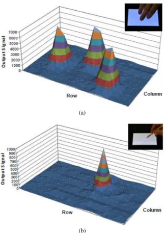
A 5inch WSVGA in-cell touch panel LCD with the structure described above has been fabricated and the performance improvements experimentally verified. We can select either sensing scheme simply by changing the driving method of the display. Figure 12 shows the measured SNR. This SNR is defined as the ratio between the touch signal and the stan- dard deviation of the background noise level (1σ). Figure 13 shows an example of the output signal profile generated by
Fig. 12 Measured SNR.
(a)
(b)
Fig. 13 (a) Signal profile of finger touch. (b) Signal profile of pen touch.
fingers with sensing in the V-blank period (Fig. 13(a)) and a stylus with sensing in the 1H period (Fig. 13(b)).
In the case of sensing in the V-blank period, the mea- sured SNR was found to be 257 using a finger (10 mmφ Slug) and 32 using a small tipped conductive stylus (2 mmφ). The report rate of touch panel was 60 Hz. In the case of sensing in the 1H period, the measured SNR was 211 using a finger (10 mmφSlug) and 28 using a small tipped conductive stylus (2 mmφ). The report rate of touch panel was 144 Hz. Accordingly, high SNR operation of the touch panel was confirmed for both finger and pen input.
In the case of sensing in the V-blank period, a driv- ing frequency of 120 Hz was achieved with the prototype LCD. However, with the development of 240 Hz LCD driv- ing technologies [9], this sensing scheme will enable an im- provement of the report rate (>120 Hz) and higher a SNR due to the subsequent increase in the number of samples per frame. The V-blank period sensing scheme can also be com- bined with a low frame rate LCD driving technology that becomes possible by using IGZO TFTs [8]. This approach enables higher SNR of touch panel, low power consumption of the display and enlargement of display size.
We have confirmed that our proposed method of sens- ing in the 1H period enables a longer sensing period, a greater increase in the number of samples per frame, and a higher SNR than the conventional technique of sensing in the 1H-blank period. We have also confirmed that the com- mon ITO of the VA-mode LCD enables a high SNR without
Fig. 14 Estimation for large display size.
display interference.
5.2 Display Size
The potential for applying our In-Cell capacitive touch panel technology to a large display size was estimated by simula- tion based on the measurement results from the 5inch pro- totype as shown in Fig. 14. The upper x-axis of the figure represents the display size using one side edge wiring and the lower x-axis of the figure represents the display size us- ing both side sensor-edges wiring. The simulation results show that our in-cell touch panel technology using the metal wiring on both side edges of the sensing electrodes and op- timization of process condition will enable stylus pen input up to 14inch display size and finger touch input up to 20inch display size. The sensor of the 5inch prototype is connected to TP controller by using metal wiring on one side edge of the sensor electrodes. By adapting metal wiring on both side edges, RC can be halved and thus the display size should be doubled. In other words, the TP of 10-inch display with metal wiring on both side edges have same RC constant as that of a 5-inch TP with one-side-edge metal wiring. Our simple proposed structure and sensing scheme will there- fore enable an enlargement of the display size beyond cur- rent limits.
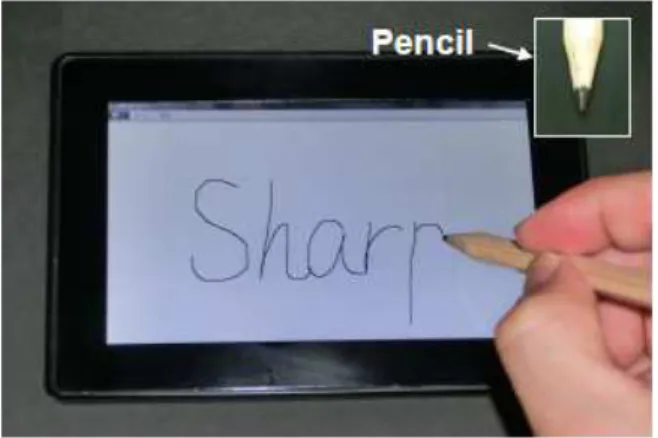
Figure 15 shows a photograph of our In-Cell touch panel with VA-Mode LCD in operation. Specifications of the prototype are shown in Table 2. The in-cell touch panel enables the use of a single FPC. This is because the seal contact allows the sensor electrodes to be connected with the electrode on the TFT substrate. Good display quality results from the reduction of reflectivity and higher trans- mittance which is a result of the reduction of the number of inter-layer interfaces.
6. Conclusion
We have described an In-Cell Projected Capacitive Touch
Fig. 15 Photograph of prototype LCD.
Table 2 Display specifications.
Panel in a display using IGZO TFT technology. The suc- cess of increasing the SNR of the In-Cell touch panel en- ables pen input operation, lower cost and an enlargement of the display size. The possibility of enlarging the display size makes this a highly promising approach for In-Cell Capaci- tive type touch panels.
7. Future Work
In future, we aim to combine our sensing scheme with the low frame rate technology made possible by using IGZO TFTs [8]. This approach enables higher SNR of touch panel and reduces the power consumption of the display.
Although we have demonstrated a 5-inch WSVGA panel, in theory the proposed in-cell touch panel display can also be applied to tablet PCs (10-inch) and PC moni- tor (about 24-inch). Therefore, we are planning to fabricate an In-cell touch panel LCD with a large display size for use as a PC monitor.
Acknowledgments
The authors thank H. Kato, H. Ogawa, C. Brown and H. Kawamori for their encouragement and invaluable tech- nical advice.
[5] C. Brown, et al., “A system LCD with integrated 3-Dimensional input device,” SID 2010, pp.453–456, 2010.
[6] S. Tomita, et al., “An in-cell capacitive touch-sensor integrated in an LTPS WSVGA TFT-LCD,” SID 2011 Digest, pp.629–632, 2011.
[7] K. Noguchi, et al., “Novel in-cell capacitive touch panel technology in a wide viewing angle IPS-mode display,” EuroDisplay 2011, S11.3, 2011.
[8] S. Amano, et al., “Low power LC display using In-Ga-Zn-Oxide TFTs based on variable frame frequency,” SID 2010, pp.626–629, 2010.
[9] Y. Yamada, et al., “Advanced technologies for 3D liquid crystal tele- vision,” SID 2011, pp.160–163, 2011.
Yasuhiro Sugita received his B.Eng. and M.Eng. degrees in electronics engineering from Hosei University, Tokyo, Japan, in 1995 and 1997, respectively. He joined Sharp Corp., Japan, in 1997, where he has been engaged in the research on devices and circuits for high- density flash memory, RRAM, and embedded non-volatile memory, and began researching in- tegrated sensors for system displays in 2008. He is now a member of the Corporate Research and Development Group, Sharp Corp., Nara, Japan, where he is developing touch-panel technologies and large-area electronics for display devices.
Kazutoshi Kida received his B.Eng. and M.eng. degrees in bioinformatic engineering from Osaka University, Osaka, Japan, in 1993 and 1995, respectively. He joined Sharp Corp., Japan, in 1995, where he has been engaged in developing LCD, and began researching inte- grated sensors for system displays in 2008. He is now a member of the Electronic Components And Devices Group, Sharp Corp., Nara, Japan, where he is developing touch-panel technolo- gies.
Shinji Yamagishi received the B.S. degree in applied chemistry engineering from Yama- nashi University in 1992. He joined Sharp Corp., Japan, in 1992, where he has been en- gaged in the research on liquid crystal material and module technology for LCD. He is now a member of the Corporate Research and Devel- opment Group, Sharp Corp., Nara, Japan, where he is developing touch-panel technologies.