INVITED PAPER
Special Section on Analog Circuits and Related SoC Integration TechnologiesExtremely Low Power Digital and Analog Circuits
Hirofumi SHINOHARA†a),Member
SUMMARY Extremely low voltage operation near or below threshold voltage is a key circuit technology to improve the energy efficiency of in- formation systems and to realize ultra-low power sensor nodes. However, it is difficult to operate conventional analog circuits based on amplifier at low voltage. Furthermore, PVT (Process, Voltage and Temperature) vari- ation and randomVth variation degrade the minimum operation voltage and the energy efficiency in both digital and analog circuits. In this paper, extremely low power analog circuits based on comparator and switched ca- pacitor as well as extremely low power digital circuits are presented. Many kinds of circuit technologies are applied to cope with the variation problem.
Finally, image processing SoC that integrates digital and analog circuits is presented, where improvement of total performance by a cooperation of analog circuits and digital circuits is demonstrated.
key words: sub-threshold, near-threshold, energy efficiency, extremely low voltage, extremely low power
1. Introduction
Energy efficiency is one of the most important features for every information equipment, and its importance is getting higher as the total bit count transferred and stored around the world increase. In order to improve the energy efficiency a lot of works have been done on sub-threshold circuits and near-threshold circuits mostly in the fields of digital logic and memory [1]–[4]. However the effects of PVT variation and randomVth variation become much severer at the ex- tremely low voltage operation. There exists a requirement of extremely low power analog circuits with extremely low voltage operation in two meanings. One is to be integrated in the same SoC and keeps the high energy efficiency. An- other is to help the digital circuits cope with the variation problems.
In this paper, after showing the ideal dependence of the energy efficiency on supply voltageVDD, misfits to the ideal curve in the real circuits are categorized in three types and discussed. Then specific extremely low power circuits both digital and analog are explained. Finally advantages of col- laborated works between digital circuits and analog circuits are presented.
2. Energy Characteristics Ideal and Real
Energy consumption of LSI for a certain task is obtained by its PD product (product of power and delay). In case of
Manuscript received February 8, 2014.
Manuscript revised March 3, 2014.
†The author is with Semiconductor Technology Academic Re- search Center (STARC), Yokohama-shi, 222-0033 Japan.
a) E-mail: [email protected] DOI: 10.1587/transele.E97.C.469
Fig. 1 Dependence of energy consumption onVDD.
CMOS logic circuits it is expressed as Eq. (1) Etotal =PD∝αCV2DD+IleakVDD
f (1)
whereαis an activation ratio
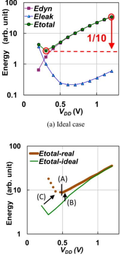
The first term and the second term of (1) represent dynamic energy Edyn due to dynamic current and static leak energy Eleak due to leakage currentIleak,respectively. Figure 1(a) shows dependences of the energy onVDDin the ideal case.
AsVDD goes down from nominal value of 1.2 V,Etotal de- creases in proportion toVDD2 , becauseEdyndominate in the highVDDregion. WhenVDDis further decreased and MOS- FET operate at near-threshold region or sub-threshold re- gion, cycle frequency f becomes so small that increase of Eleak cannot be neglected. Finally the increase ofEleak out- weighs the decrease ofEdyn. This means that there is a min- imum value inEtotallimited by the leak current. The mini- mumEtotalis reduced to around 1/10 from the nominalVDD
Copyright c2014 The Institute of Electronics, Information and Communication Engineers
(C) MinimumEtotalappears at higherVDDand is larger than ideal.
These deviations are caused by many reasons such as PVT variation, random Vth variation, circuit overhead to cope with them, no rail-to-rail swing operation, DC current, mismatch of optimum operation condition between macro blocks, etc. The deviations are discussed specifically in Sect. 3.
3. Extremely Low Voltage Building Block Circuits In this section, representative digital and analog circuits are picked up, and the deviations mentioned above are ex- plained in response to the circuit operations and resent re- search results against them are presented.
3.1 Logic
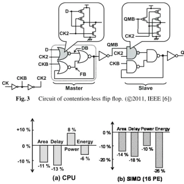
CMOS logic circuits are known to be functional at relatively low voltage. It is still not low enough for extremely low voltage operation in a large scale logic macro. It is ob- served that minimum functional voltageVDDmin of primi- tive circuit increases as number of the gate stage increases as shown in Fig. 2. In the combinational circuits malfunc- tion is caused by stochastic mismatch between output volt- age and logical input threshold voltage, and expected value ofVDDmin for CMOS inverter chain is expressed as Eq. (2) [5]. Dependences on σpn andN are explicitly expressed here. And guides for device parameters are derived from this equation; smallernand smaller|η|are better. As can be seen from Fig. 2, flip flop has the largestVDDmin, and brings the deviation (A). The stochastic error in flip flop is investi- gated and the signal contention at the data feed-back point is found to be a main factor. In order to improve theVDDmin
a contention-less flip flop (CLFF) illustrated in Fig. 3 is pro- posed [6].
Fig. 2 Dependence ofVDDminon number of gate stages.
β: Intrinsic strength
η: DIBL (Drain Induced Barrier Lowering) coefficient UT: Thermal Voltage
σpn: Within-die Vth variation
A 16 bit arithmetic unit including CLFF showed func- tionality below the energy optimum VDD, and achieved>
10x improvement of energy efficiency compared with it at the nominalVDDof 1.2 V.
Another challenge for logic circuits is a timing closure at the extremely low voltage corner in a SoC design flow.
Since the on chip timing variation increases more severely than average timing delay, a lot of delay buffers are required to insert in the logic and clock circuits. This lead to a heavy circuit overhead that causes deviation (B) and enlargement of cycle time that leads to deviation (C). In order to smooth the timing closure procedure, high voltage clock distribution (HVCD) technic is proposed [7]. Although HVCD requires two supply voltages;VCLKandVLOGIC(VCLK >VLOGIC), it decreases the number of delay buffers. As a result, improve- ments of area, delay and energy (PD product) are achieved in 32 bit CPU macro and SIMD macro as shown in Fig. 4.
3.2 Memory
SRAM is one of the most sensitive circuits to the random Vthvariation, because it degrades both bit cell stability dur-
Fig. 3 Circuit of contention-less flip flop. ( c2011, IEEE [6])
Fig. 4 Effects of HVCD. ( c2013, IEEE [7])
Fig. 5 Variation of bit line waveforms. ( c2011, IEEE [10])
Fig. 6 Hierarchical bit line circuit for charge share. ( c2011, IEEE [10])
ing a read operation and a write margin. So, many kinds of assist circuits have been proposed to improve the stability and/or the write margin so as to overcome aVDDminproblem (deviation (A)) [8], [9]. From a view point of low energy, however, problem is not justVDDmin. Charging/discharging current of bit lines do not decrease ideally owing to a ran- dom variation of bit cell read current, and deviation (B) oc- curs. As shown in Fig. 5 the bit line swing in a read op- eration, which is normally small amplitude at the nominal voltage (a), vary widely at the extremely low voltage (b).
The average swing becomes rather lager in Fig. 5(b).
In order to reduce the variation of bit line swing, an ap- proach that focuses to the bit line charge is proposed. Fig- ure 6 shows an example hierarchical bit line circuit [10].
Here, the charge of local bit line (LBL, LBLX) with small capacitance, is transferred to and shared by global bit line (GBL, GBLX) with large capacitance. Thus the variation of global bit line swing is suppressed and the operation power at 0.5 V is reduced by 60%.
The charge focused approach is further advanced to charge collector circuit shown in Fig. 7 [11]. In addition to the charge of selected bit line, that of unselected bit line is also collected to the global bit line. This highly efficient charge usage yields drastic power reduction in large scale SRAM.
3.3 Power Management
It is well known that performance of operational amplifier degrades much at low voltage, and finally it does not oper-
Fig. 7 Charge collector circuit. ( c2012, IEEE [11])
Fig. 8 Digital LDO circuit. ( c2010, IEEE [12])
ate (deviation (A)). Even if it operates, its DC current acts like the leak current Ileakin Eq. (1) and causes deviation (C). Thus analog circuits that utilize comparator instead of amplifier have been investigated.
Figure 8 shows a circuit of comparator based digital LDO (Low Drop Out) [12]. Number of turn on power tran- sistors is controlled by output of the comparator and con- trol logic. Measured VOUT-VIN characteristics at the load current of 200μA is shown in Fig. 9. The digital LDO suc- cessfully regulatesVOUTfrom 0.35 to 0.45 V atVIN=0.5 V.
At VOUT =0.45 V and VIN = 0.5 V, the line regulation is 3.1 mV/V.
3.4 PLL
In the area of PLL, all digital (AD) PLL is becoming a popu- lar circuit style. Figure 10 shows a block diagram of a 0.5 V AD-PLL [13]. Current controlled ring oscillator is applied to DCO (Digitally Controlled Oscillator) to obtain power scalability, which means variable power proportional to fre- quency. Timing edges for TDC (Time to Digital Converter) are generated by level shifters from multi-phase output of the DCO. The waveform of DCO outputs have low “H” level and low slew rate so that the accuracy to detect the phase difference would be degraded if it was directly connected to TDC. The level shifters sharpen the waveform and avoid the
Fig. 9 Output characteristic of digital LDO. ( c2010, IEEE [12])
Fig. 10 Block diagram of 0.5 V AD-PLL. ( c2012, IEEE [13])
Fig. 11 Measured power consumption of proposed AD-PLL. ( c2012, IEEE [13])
problem even at as low as 0.5 V. As illustrated in Fig. 11, the AD-PLL is power scalable from 10 MHz to 100 MHz. The power efficiency is less than 0.5μW/MHz in this frequency region.
3.5 RF Transceiver
For the application of short-range wireless, all 0.5 V, 1 Mbps, 315 MHz OOK transceiver is developed [14]. In order to reduce the RX (Receiver) power, (1) sampling cir- cuits are used and the RX input is directly sampled without LNA (Low Noise Amplifier) (high sensitivity is not required for the 1-m communication), (2) low career frequency of 315 MHz instead of 2.4 GHz is used to reduce the required bandwidth of the sampler, (3) the power supply voltage (VDD) is reduced to 0.5 V, (4) a career-frequency-free (CFF) intermittent sampling (IS) is newly proposed to reduce the number of sampling. Concepts of a conventional continu-
Fig. 12 Comparison of sampling concept. ( c2012, IEEE [14])
Fig. 13 Block diagram of career-frequency-free (CFF) IS RX. ( c2012, IEEE [14])
ous sampling and the proposed IS are compared in Fig. 12.
The proposed IS reduces the number of the sampling in 1 symbol that makes the power consumption in sampler to 1/315. Figure 13 shows a block diagram of the proposed all 0.5 V CFF IS RX. Only 1-MHz clock instead of a 315- MHz career frequency is supplied to RX. Power consump- tion of the samplers in RX is 3μW and the total RX con- sumes 38μW@1 Mbps (38 pJ/bit). At BER of 10−3, the RX sensitivity is−55 dBm.
The design challenge of TX (Transmitter) is to increase the efficiency at the target low output power of−20 dBm. A class-F PA instead of a class-D or class-E PA is used, be- cause it achieves the highest efficiency at the target speci- fication. Furthermore a dual supply voltage scheme is pro- posed as shown in Fig. 14 [15]. By applyingVDD1=0.56 V, VDD2=0.2 V drain efficiency of 42% is achieved, which is 2.1 times larger than that at single 0.5 VVDD. The global efficiency of 28% is highest at POUT =−20 dBm. Energy efficiency of 36 pJ/bit (36μW@1 Mbps) is achieved.
4. Digital and Analog Corporation in Integrated Chip In this section, collaborated works between digital circuits and analog circuits that improve total performance and en- ergy efficiency are presented.
Fig. 14 Schematic of a dualVDDTX with a class-F PA. ( c2012, IEEE [15])
Fig. 15 Block diagram of adaptive supply voltage control based on setup error prediction. ( c2012, IEEE [16])
4.1 Adaptive Supply Voltage Control
Commercial SoC is required to operate at its specified max- imum frequency (Fmax) at the worst PVT condition. For a fast corner low-Vthchip, Fmax is limited to much slower value than its ability. Then the product of the leak power and the cycle time becomes larger than expected. This deviation is significant in the lowVDDregion, and it is categorized as the deviation (C).
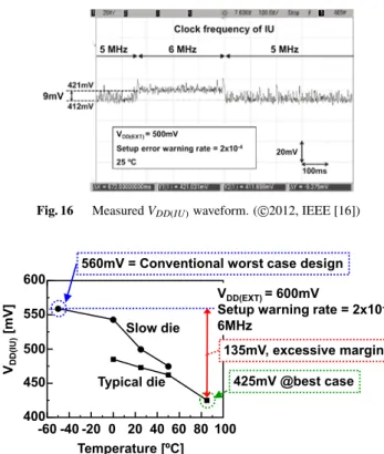
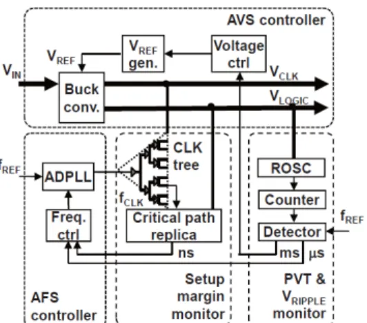
In order to avoid the mismatch between Fmax and a chip’s ability, adaptiveVDD control with parity-based error prediction and detection (PEPD) is prosed [16]. Block di- agram including integer units, warning rate calculator, and digital LDO is shown in Fig. 15. The digital LDO shown in Sect. 3Cis utilized here. According to the clock frequency setup warning rate is calculated, and the output of the digital LDO (VDD(IU)) is controlled to the optimum voltage. Fig- ure 16 shows measuredVDD(IU) waveform. As input clock frequency increses from 5 MHz to 6 MHz, and decreases from 6 MHz to 5 MHz,VDD(IU) is adaptively-controlled up and down by 9 mV respectively.
Figure 17 shows measured adaptive VDD(IU) for dif- ferent dies and different temperatures. The lowest volt- age @6 MHz is 425 mV for typical die at high temperature.
In conventional worst-case design, the worst caseVDD(IU)
(=highest) of 560 mV should be applied to the best case. Ex-
Fig. 16 MeasuredVDD(IU)waveform. ( c2012, IEEE [16])
Fig. 17 Measured adaptiveVDDcontrol vs. temperature. ( c2012, IEEE [16])
Fig. 18 Comparison of measured power. ( c2012, IEEE [16])
cessiveVDDmargin of 135 mV is eliminated by this adaptive VDDcontrol. This yields 13% total power reduction includ- ing the overhead of PEPD and LDO loss as illustrated in Fig. 18. If the LDO loss is not accounted for, the power re- duction should be 38%.
4.2 Adaptive Voltage and Frequency Control
Another collaborate work between digital and analog is adaptive voltage scaling (AVS) and adaptive frequency scal- ing (AFS) with monitor circuits, power management (buck converter), and AD-PLL. Its block diagram is illustrated in Fig. 19 [7]. The AD-PLL shown in Sect. 3Dis utilized here.
Die-to-die process variation and temperature varia- tion are compensated by AVS. Frequency of ring oscillator (ROSC) is compared with a reference frequency (fREF), and
Fig. 19 Block diagram of adaptive voltage and frequency scaling.
( c2013, IEEE [7])
Fig. 20 Measured waveforms ofVLOGIC and fCLKwith AFS. ( c2013, IEEE [7])
an up/down signal is given to the AVS controller every sev- eral 10 ms to controlVLOGICandVCLKagainst the variations.
By using proposed AFS, fCLKtracks a several 100μs- order VLOGIC noise which is often observed at high effi- ciency DC/DC converter. Another up/down signal is given to the AFS controller every about 10μs, and a multiplica- tion number in the AD-PLL is changed to tune fCLK. Criti- cal path replicas also monitorVLOGICevery cycle by check- ing the setup margin. When a setup warning is found, the critical-path-replica interrupts the up/down signal to avoid a setup error. Figure 20 shows measured waveforms of VLOGIC and fCLK with AFS. A 4 kHz sinusoidal wave is applied toVLOGIC to emulate the ripple of the buck con- verter. The proposed AFS makes fCLK trackVLOGIC, and increases the average clock frequency by 33% compared to the conventional worst case design. Proposed AVS, AFS and HVCD in Sect. 3.1 are applied to an image processing SoC [7]. AtVLOGIC=0.45 V,VCLK=5.65 V the SIMD core achieved the maximum power efficiency of 563GOPS/W.
Die photograph fabricated with 40 nm CMOS process is shown in Fig. 21.
Fig. 21 Die photograph of image processing SoC. ( c2013, IEEE [7])
5. Conclusion
Extremely low voltage operation is a key approach to im- prove the energy efficiency. Deviations of energy curve in a real SoC from ideal case are categorized in three cases.
They are discussed in several specific digital circuits and analog circuits. And it is demonstrated that by using proper circuit countermeasures, both analog and digital circuits can operate at the sub-threshold or near-threshold voltage and they can exhibit low energy characteristics. Finally, exam- ples of collaborative works between digital circuits and ana- log circuits showed that they were effective in eliminating the excessiveVDD margin and fCLK margin required in the conventional worst case design to realize high total energy efficiency.
Acknowledgments
This work was carried out as part of the Extremely Low Power (ELP) project supported by the Ministry of Economy, Trade and Industry (METI) and the New Energy and Indus- trial Technology Development Organization (NEDO).
References
[1] A. Wang and A. Chandrakasan, “A 180-mV subthreshold FFT pro- cessor using a minimum energy design methodology,” IEEE J.
Solid-State Circuits, vol.40, no.1, pp.310–319, Jan. 2005.
[2] B.H. Calhoun and A.P. Chandrakasan, “A 256-kb 56-nm sub- threshold SRAM design for Ultra-Low-voltage operation,” IEEE J.
Solid-State Circuits, vol.42, no.3, pp.680–688, March 2007.
[3] B. Zhai, L. Nazhandali, J. Olson, A. Reeves, M. Minuth, R. Helfand, S. Pant, D. Blaauw, and T. Austin, “A 2.60 pJ/Inst subthreshold sen- sor processor for optimal energy efficiency,” IEEE 2006 Symposium on VLSI Circuits, pp.154–155, June 2006.
[4] H. Kaul, M. Anders, S. Mathew, S. Hsu, A. Agarwal, R. Krishna- murthy, and S. Borkar, “A 320 mV 56μW 411GOPS/Watt ultra-low voltage motion estimation accelerator in 65 nm CMOS,” IEEE 2008 ISSCC, pp.316–317, Feb. 2008.
[5] H. Fuketa, S. Iida, T. Yasufuku, M. Takamiya, M. Nomura, H.
Shinohara, and T. Sakurai, “A closed-form expression for estimat- ing minimum operating voltage (VDDmin) of CMOS logic gates,”
2011 DAC, pp.984–989, June 2011.
[6] H. Fuketa, K. Hirairi, T. Yasufuku, M. Takamiya, M. Nomura, H.
Shinohara, and T. Sakurai, “12.7-times energy efficiency increase of 16-bit integer unit by power supply voltage (VDD) scaling from 1.2 V to 310 mV enabled by contention-less flip-flops (CLFF) and separated VDD between flip-flops and combinational logics,” IEEE 2011 ISLPED, pp.163–168, Aug. 2011.
[7] M. Nomura, A. Muramatsu, H. Takeno, S. Hattori, D. Ogawa, M.
Nasu, K. Hirairi, S. Kumashiro, S. Moriwaki, Y. Yamamoto, S.
Miyano, Y. Hiraku, I. Hayashi, K. Yoshioka, A. Shikata, H. Ishikuro, M. Ahn, Y. Okuma, X. Zhang, Y. Ryu, K. Ishida, M. Takamiya, T.
Kuroda, H. Shinohara, and T. Sakurai, “0.5 V image processor with 563 GOPS/W SIMD and 32 bit CPU using high voltage clock dis- tribution (HVCD) and adaptive frequency scaling (AFS) with 40 nm CMOS,” IEEE 2013 Symposium on VLSI Circuits, pp.36–37, June 2013.
[8] K. Zhang, U. Bhattacharya, Z. Chen, F. Hamzaoglu, D. Murray, N. Vallepalli, Y. Wang, B. Zheng, and M. Bohr, “A 3-GHz 70-Mb SRAM in 65-nm CMOS technology with integrated column based dynamic power supply,” IEEE J. Solid-State Circuits, vol.41, no.1, pp.146–151, Jan. 2006.
[9] S. Ohbayashi, M. Yabuuchi, K. Nii, Y. Tsukamoto, S. Imaoka, Y.
Oda, T. Yoshihara, M. Igarashi, M. Takeuchi, H. Kawashima, Y.
Yamaguchi, K. Tsukamoto, M. Inuishi, H. Makino, K. Ishibashi, and H. Shinohara, “A 65-nm SoC embedded 6T-SRAM designed for manufacturability with read and write operation stabilizing circuits,”
IEEE J. Solid-State Circuits, vol.42, no.4, pp.820–829, April 2007.
[10] S. Moriwaki, A. Kawasumi, T. Suzuki, T. Sakurai, and S. Miyano,
“0.4 V SRAM with bit line swing suppression charge share hierar- chical Bit line scheme,” IEEE 2011 CICC, M-6.S, Sept. 2011.
[11] S. Moriwaki, Y. Yamamoto, A. Kawasumi, T. Suzuki, S. Miyano, T. Sakurai, and H. Shinohara, “A 13.8 pJ/access/Mbit SRAM with charge collector circuits for effective use of non-selected bit line charges,” IEEE 2012 Symposium on VLSI Circuits, pp.60–61, June 2012.
[12] Y. Okuma, K. Ishida, Y. Ryu, X. Zhang, P.H. Chen, K. Watanabe, M. Takamiya, and T. Sakurai, “0.5-V input digital LDO with 98.7%
current efficiency and 2.7-μA quiescent current in 65 nm CMOS,”
IEEE 2010 CICC, pp.323–326, Sept. 2010.
[13] Y. Hiraku, I. Hayashi, H. Chung, T. Kuroda, and H. Ishikuro, “A 0.5 V 10 MHz-to-100 MHz 0.47μW/MHz power scalable AD-PLL in 40 nm CMOS,” IEEE 2012 A-SSCC, pp.33–36, Nov. 2012.
[14] A. Saito, K. Honda, Y. Zheng, S. Iguchi, K. Watanabe, T. Sakurai, and M. Takamiya, “An all 0.5 V, 1 Mbps, 315 MHz OOK transceiver with 38-μW career-frequency-free intermittent sampling receiver and 52-μW class-F transmitter in 40-nm CMOS,” IEEE 2012 Sym- posium on VLSI Circuits, pp.38–39, June 2012.
[15] S. Iguchi, A. Saito, K. Watanabe, T. Sakurai, and M. Takamiya, “2.1 times increase of drain efficiency by dual supply voltage scheme in 315 MHz class-F power amplifier at output power of−20 dBm,”
IEEE 2012 ESSCIRC, pp.345–348, Sept. 2012.
[16] K. Hirairi, Y. Okuma, H. Fuketa, T. Yasufuku, M. Takamiya, M.
Nomura, H. Shinohara, and T. Sakurai, “13% power reduction in 16b integer unit in 40 nm CMOS by adaptive power supply voltage control with parity-based error prediction and detection (PEPD) and fully integrated digital LDO,” IEEE 2012 ISSCC, pp.485–486, Feb.
2012.
Hirofumi Shinohara received B.S. and M.S. degrees in electrical engineering and Ph.D.
degree in informatics from Kyoto University, in 1976, 1978, and 2008, respectively. In 1978, he joined the LSI Laboratory of Mitsubishi Elec- tric Corporation, where he was involved in re- search and development of MOS SRAMs, mem- ory compilers and logic building blocks. From 2003 to 2009 he was engaged in development of basic logic circuits, memory macros and design methodology for advanced CMOS technologies in Renesas Technology Corporation. In 2009 he moved to Semiconductor Technology Research Academic Center (STARC), where he directed a joint research project on extremely low power circuits and systems with universi- ties in Japan. He is currently engaged in an administration of collaborative researches on VLSI circuits between industry and academy. His research interests include advanced SRAM, low-power circuits, and variation-aware design. He is a member of IEICE.
![Fig. 5 Variation of bit line waveforms. ( c 2011, IEEE [10])](https://thumb-ap.123doks.com/thumbv2/123deta/5625952.1500219/3.892.478.804.126.499/fig-variation-bit-line-waveforms-c-ieee.webp)
![Fig. 10 Block diagram of 0.5 V AD-PLL. ( c 2012, IEEE [13])](https://thumb-ap.123doks.com/thumbv2/123deta/5625952.1500219/4.892.104.398.114.306/fig-block-diagram-v-ad-pll-c-ieee.webp)