NI PXIe-5451 Specifications
400 MS/s Two-Channel Arbitrary Waveform Generator
This document lists specifications for the NI PXIe-5451 (NI 5451) arbitrary waveform generator.
Specifications are warranted under the following conditions: • 15 minutes warm-up time at ambient temperature • Calibration cycle maintained
• Chassis fan speed set to High • NI-FGEN instrument driver used
• NI-FGEN instrument driver self-calibration performed after instrument is stable
Unless otherwise noted, the following conditions were used for each specification:
• Signals terminated with 50Ω to ground
• Main path set to 2.5 Vpk differential (gain = 2.5, 5 Vpk-pk differential)
• Direct path set to 0.5 Vpk differential (gain = 0.5, 1 Vpk-pk differential)
• Sample clock rate set to 400 MS/s
• Onboard Sample clock used, with no Reference clock • Analog filter enabled
• 0 °C to 55 °C ambient temperature
Specifications describe the warranted, traceable product performance over
ambient temperature ranges of 0 °C to 55 °C, unless otherwise noted.
Typical values describe useful product performance beyond specifications
that are not covered by warranty and do not include guardbands for measurement uncertainty or drift. Typical values may not be verified on all units shipped from the factory. Unless otherwise noted, typical values cover the expected performance of units over ambient temperature ranges of 23 ±5 °C with a 90% confidence level, based on measurements taken during development or production.
Nominal values (or supplemental information) describe additional
information about the product that may be useful, including expected performance that is not covered under Specifications or Typical values. Nominal values are not covered by warranty.
Specifications are subject to change without notice. For the most recent NI 5451 specifications, visit ni.com/manuals.
To access all the NI 5451 documentation, navigate to Start» All Programs»National Instruments»NI-FGEN»Documentation.
Hot Surface If the NI 5451 has been in use, the device or the shield may exceed safe handling temperatures and may cause burns. Allow the NI 5451 to cool before touching the shield or removing the device from the chassis.
Electromagnetic Compatibility Guidelines
This product was tested and complies with the regulatory requirements and limits for electromagnetic compatibility (EMC) as stated in the product specifications. These requirements and limits are designed to provide reasonable protection against harmful interference when the product is operated in its intended operational electromagnetic environment. This product is intended for use in industrial locations. There is no guarantee that harmful interference will not occur in a particular
installation, when the product is connected to a test object, or if the product is used in residential areas. To minimize the potential for the product to cause interference to radio and television reception or to experience unacceptable performance degradation, install and use this product in strict accordance with the instructions in the product documentation.
Furthermore, any changes or modifications to the product not expressly approved by National Instruments could void your authority to operate it under your local regulatory rules.
Caution For EMC compliance, you must install PXI EMC Filler Panels, National Instruments part number 778700-01, in all open chassis slots.
Contents
Electromagnetic Compatibility Guidelines ... 2
Analog Outputs ... 4
CH 0+/–, CH 1+/– (Analog Outputs, Front Panel Connectors)... 4
Clocking ... 40
Onboard Sample Clock ... 40
External Sample Clock ... 42
External Sample Clock Timebase... 44
Exporting Clocks ... 45
Terminals ... 45
CLK IN (Sample Clock and Reference Clock Input, Front Panel Connector) ... 45
CLK OUT (Sample Clock and Reference Clock Output, Front Panel Connector) ... 46
PFI 0 and PFI 1 (Programmable Function Interface, Front Panel Connectors) ... 47
Triggers and Events ... 49
Triggers ... 49
Events... 51
Waveform Generation Capabilities... 52
Onboard Signal Processing ... 55
Calibration... 60
Power ... 60
Software ... 61
Physical ... 62
Hardware Front Panel ... 62
NI PXIe-5451 Environment ... 64
Compliance and Certifications... 65
Safety ... 65
Electromagnetic Compatibility ... 65
CE Compliance ... 65
Online Product Certification ... 65
Environmental Management... 66
Analog Outputs
CH 0+/–, CH 1+/–
(Analog Outputs, Front Panel Connectors)
Specification Value Comments
Number of Channels
2 —
Output Type Single-ended, differential Single-ended
output available on Main path only.
Output Paths Main path, Direct path —
The following figure illustrates the relationship between the differential offset voltage and the common-mode offset voltage, along with a generated peak-to-peak AC signal for single-ended and differential configurations. The peak-to-peak differential receiver voltage rejects the common-mode offset voltage and other common-mode noise present in the signal.
Figure 1. Definition of Common Mode Offset and Differential Offset
VPPD =VPPSE+ + VPPSE–
where VPPD represents the differential peak-to-peak voltage
VPPSE represents the single-ended peak-to-peak voltage
VDO represents the differential offset voltage
VCMO represents the common-mode offset voltage
Note The instantaneous differential voltage is equal to Output (CH+) – Output (CH–). Output offset settings are independent of gain settings.
VPPSE+ VPPSE– 0V VCMO VDO Output (VMAX) Output (CH+) Output (CH–) Output (VMIN) VPPD
+
–
VDO CH 0+ CH 0–Specification Value Comments Amplitude and Offset
Full-Scale Amplitude Range*
Single-Ended Main Path Measured on
CH+. Vpk on each terminal is equal to analog offset + waveform data × gain. Flatness Correction State Load Amplitude (VPPSE)† Minimum Value Maximum Value Disabled 50Ω 0.00176 2.50 1 kΩ 0.00336 4.76 Open 0.00352 5.00 Enabled 50Ω 0.00124 1.75 1 kΩ 0.00235 3.33 Open 0.00247 3.50
Differential Main Path Measured as
differential peak-to-peak signal amplitude (Vpk-pk). Each terminal Vpk-pk is half of the differential Vpk-pk. Vpk on each terminal is equal to differential offset × 0.5 + common-mode offset + waveform data × gain/2. Flatness Correction State Load Amplitude (VPPD)† Minimum Value Maximum Value Disabled 50Ω 0.00352 5.00 1 kΩ 0.00671 9.52 Open 0.00705 10.00 Enabled 50Ω 0.00247 3.50 1 kΩ 0.00470 6.66 Open 0.00493 7.00
Notes: For all configurations, both CH± terminals are terminated to ground through loads of the same value.
The voltage output levels are set in the software and are based on a 50 Ω per line load termination to ground (the default)or
based on the user-specified load resistance. Common-mode offset assumes output terminals are terminated into equal loads to ground. Refer to the NI Signal Generators Help and navigate to NI Signal Generators Help»Devices»NI 5451»Front Panel Connectors»Differential and Single-Ended Channel Connectors for more information.
Gain values in NI-FGEN correspond to Vpk,which is half the amplitude in Vpk-pk.
* Combinations of waveform data, offset, and gain that exceed a single-ended peak output voltage of 3.2 V may result in
waveform clipping.
† Amplitude values assume the full scale of the DAC is used. If an amplitude smaller than the minimum value is desired, you
can use waveforms less than the full scale of the DAC, or you can use digital gain. Additional offset can be added using waveform data.
Amplitude and Offset (Continued) Full-Scale
Amplitude Range*
Differential Direct Path Both CH 0+/– or CH 1+/– terminals are terminated to ground through loads of the same value.
Single-ended values are half of differential values. Flatness Correction State Load Amplitude (VPPD)† Minimum Value Maximum Value Disabled 50Ω 0.708 1.00 1 kΩ 1.35 1.90 Open 1.42 2.00 Enabled 50Ω 0.567 0.8 1 kΩ 1.08 1.52 Open 1.14 1.6 Amplitude Resolution 4 digits <0.0025% (0.0002 dB of amplitude range) —
Notes: For all configurations, both CH± terminals are terminated to ground through loads of the same value.
The voltage output levels are set in the software and are based on a 50 Ω per line load termination to ground (the default)or
based on the user-specified load resistance. Common-mode offset assumes output terminals are terminated into equal loads to ground. Refer to the NI Signal Generators Help and navigate to NI Signal Generators Help»Devices»NI 5451»Front Panel Connectors»Differential and Single-Ended Channel Connectors for more information.
Gain values in NI-FGEN correspond to Vpk,which is half the amplitude in Vpk-pk.
* Combinations of waveform data, offset, and gain that exceed a single-ended peak output voltage of 3.2 V may result in
waveform clipping.
† Amplitude values assume the full scale of the DAC is used. If an amplitude smaller than the minimum value is desired, you
can use waveforms less than the full scale of the DAC, or you can use digital gain. Additional offset can be added using waveform data.
Amplitude and Offset (Continued) Analog Offset
Range, per Terminal
Main Path Both CH 0+/–
or CH 1+/– terminals are terminated to ground through loads of the same value. Offset is any combination of common-mode offset voltage and differential offset voltage. Load Amplitude (Vpk)*† 50Ω ±1.00 1 kΩ ±1.905 Open ±2.00 Direct Path Load Amplitude (Vpk)*† Any —
Offset Resolution Main Path Applies to
differential, common-mode, and single-ended offsets. 4 digits <0.002% of offset range
Notes: For the Main path, VCM +VDIFF/2 and VCM – VDIFF/2 is between ±2 V, into an open load.
For all configurations, both CH± terminals are terminated to ground through loads of the same value.
The voltage output levels are set in the software and are based on a 50 Ω per line load termination to ground (the default)or
based on the user-specified load resistance. Common-mode offset assumes output terminals are terminated into equal loads to ground. Refer to the NI Signal Generators Help and navigate to NI Signal Generators Help»Devices»NI 5451»Front Panel Connectors»Differential and Single-Ended Channel Connectors for more information.
* Additional offset can be added using waveform data.
† Combinations of waveform data, offset, and gain that exceed a single-ended peak output voltage of 3.2 V may result in
waveform clipping.
Specification Value Comments Accuracy
DC Accuracy Single-Ended Main Path Measured with
a DMM. Measured with both output terminals terminated to ground through a high impedance. Absolute Gain Error:
within ±5 °C of Self-Cal temperature:
±(0.4% of single-ended output range*+ 0.5 mV)
±(0.3% of single-ended output range*+ 0.3 mV), typical
outside ± 5 °C of Self-Cal temperature: – 0.05%/°C
– 0.035%/°C, typical Offset Error:
±(0.15% of offset + 0.04% of single-ended output range* +
1.25 mV) (0 °C to 55 °C)
±(0.08% of offset + 0.025% of single-ended output range* +
0.75 mV) (0 °C to 55 °C), typical
* For DC accuracy, single-ended output range is defined as 2× the gain setting into high impedance. For example, the
accuracy of a DC signal with a gain of 2.5, a load impedance of 1 GΩ, and a single-ended output range of 5 V is calculated
by the following equation:
Gain error within ±5 °C of self-cal temperature: ±(0.4% × 5 V + 0.5 mV) = ±20.5 mV
Gain error at +10 °C of self-cal temperature: ±20.5 mV – 0.05% × 5 °C × (5 V) = +8 mV/–33 mV
Specification Value Comments Accuracy (Continued)
DC Accuracy Differential Main Path Measured with
a DMM. Measured with both output terminals terminated to ground through a high impedance. Absolute Gain Error:
within ±5 °C of Self-Cal temperature:
±(0.6% of differential output range* + 1 mV)
±(0.43% × differential output range* + 500μV), typical
outside ±5 °C of Self-Cal temperature: – 0.05%/°C
– 0.035%/°C, typical Differential Offset:
± (0.3% of differential offset + 0.01% of differential output range* + 2 mV)
± (0.16% of differential offset + 0.01% of differential output range* + 1 mV), typical
Common Mode Offset:
± (0.3% of common-mode offset + 2 mV)
± (0.16% of common-mode offset + 1 mV), typical Channel-to-Channel Relative
Gain Error:
within ±5 °C of Self-Cal temperature:
±(0.66% of differential output range*+ 1.75 mV)
outside ±5 °C of Self-Cal temperature: – 0.02%/°C
– 0.01%/°C, typical
* For DC accuracy, differential output range is defined as 2× the gain setting into high impedance. For example, the accuracy
of a DC signal with a gain of 5, a load impedance of 1 GΩ, and a differential output range of 10 V is calculated by the
following equation:
Gain error within ±5 °C of self-cal temperature: ±(0.6% × 10 V + 1 mV) = ±61 mV
Gain error at + 10 °C of self-cal temperature: ±61 mV – 0.05% × 5 °C × (10 V) = +36 mV/–86 mV
Differential Offset Error: [Requested differential offset = 1 V at gain = 5] ±(0.3% × (1 V) +
Specification Value Comments Accuracy (Continued)
DC Accuracy Differential Direct Path Measured with
a DMM. Differential offset is not adjusted during self-calibration. Measured with both output terminals terminated to ground through a high impedance. Absolute Gain Error:
within ±5 °C of Self-Cal temperature: ±0.2% of differential output range*
outside ±5 °C of Self-Cal temperature: + 0.030%/°C
+ 0.015%/°C, typical
Differential Offset: ± 1 mV (0 °C to 55 °C) Common Mode Offset†: ±350 μV (0 °C to 55 °C)
Channel-to-Channel Relative Gain Error:
within ±5 °C of Self-Cal temperature: ±0.08% of differential output range*
outside ±5 °C of Self-Cal temperature: + 0.010%/°C
+ 0.005%/°C, typical
* For DC accuracy, differential output range is defined as 2× the gain setting into high impedance. For example, the accuracy
of a DC signal with a gain of 1, a load impedance of 1 GΩ, and a differential output range of 2 V is calculated by the
following equation:
Gain error within ±5 °C of self-cal temperature: ±0.2% × (2 V) = ±4 mV
Gain error at + 10 °C of self-cal temperature: 4 mV + 0.03% × 5 × (2 V) = +7 mV/–1 mV
† Direct path common-mode offset is minimized through active circuitry. Applying an external nonzero common-mode offset
to the output terminal is not recommended; however, the common-mode circuitry can sink or source up to 5 mA of common-mode bias current. Terminate both output terminals to ground through the same impedance. If the output terminals
Specification Value Comments Accuracy (Continued)
AC Amplitude Accuracy
Single-Ended Main Path Measured
using a DMM, with full-scale data into high- impedance, 50 kHz sine wave, 400 MS/s. The output range defined in DC Accuracy must be converted to VRMS by dividing by . Absolute
within ±5 °C of Self-Cal temperature:
±(0.8% of single-ended output range + 1 mVRMS)
±(0.4% of single-ended output range + 750μVRMS),
typical
Differential Main Path Absolute
within ±5 °C of Self-Cal temperature:
±(0.8% of differential output range + 1.5 mVRMS)
±(0.4% of differential output range + 1.5 mVRMS), typical
Differential Direct Path Absolute
within ±5 °C of Self-Cal temperature: ±0.5% of differential output range Channel-to-Channel, Relative
within ±5 °C of Self-Cal temperature: ±0.2% of differential output range
±0.07% of differential output range, typical
Channel-to-Channel Timing Alignment Accuracy
Main Path Direct Path ±5 °C of
self-calibration temperature. Alignment can be improved with manual adjustment by using Sample Clock Delay. 50 ps 40 ps, typical 35 ps 25 ps, typical 2 2 ( )
Specification Value Comments Output Characteristics
DC Output Resistance
Main Path Direct Path For the Direct
path only, both output terminals must be terminated with the same impedance to ground. 50Ω nominal, per connector
50Ω nominal, per connector
Return Loss Single-Ended and Differential Main Path
Single-Ended Direct Path Differential Direct Path Nominal. 30 dB, up to 20 MHz 27 dB, up to 60 MHz 12 dB, up to 135 MHz 26 dB, 5 MHz to 60 MHz 15 dB, 60 MHz to 145 MHz 35 dB, up to 20 MHz 22 dB, up to 60 MHz 12 dB, up to 145 MHz Load Impedance Compensation
Output amplitude is compensated for user-specified load impedance to ground.∗ Performed in software. Output Coupling DC — Output Enable
Software-selectable. When disabled, output is terminated with a 50Ω, 1 W resistor.
—
∗ The voltage output levels are set in the software and are based on a 50 Ω per line load termination to ground (the default)
or based on the user-specified load resistance. Common-mode offset assumes output terminals are terminated into equal loads to ground. Refer to the NI Signal Generators Help and navigate to NI Signal Generators Help»Devices» NI 5451»Front Panel Connectors»Differential and Single-Ended Channel Connectors for more information.
Specification Value Comments Output Characteristics (Continued)
Maximum Output Overload
Main Path Direct Path For the Direct
path only, both CH 0+/– or CH 1+/– terminals are terminated to ground through loads of the same value. ±12 Vpk from a 50Ω source ±8 Vpk from a 50Ω source Waveform Summing
The output terminals support waveform summing which means the outputs of multiple NI 5451 signal generators can be connected together. Clipping may occur if the summed voltage is outside of the maximum voltage range.
Specification Value Comments Frequency Response
Analog Bandwidth
Baseband Complex Baseband Typical. –3 dB,
400 MS/s. Includes DAC sinc response. Flatness correction disabled.
Main Path, Filter Disabled 180 MHz for each I and
Q output
360 MHz when used with external I/Q modulator Main Path, Filter Enabled
135 MHz for each I and Q output
270 MHz when used with external I/Q modulator Direct Path
145 MHz for each I and Q output
290 MHz when used with external I/Q modulator
Analog Filter Main Path Direct Path
7-pole elliptic filter for image suppression
4-pole filter for image suppression
Specification Value Comments Frequency Response (Continued)
Passband Flatness
Single-Ended and Differential Main Path, Filter Enabled With respect to 50 kHz into 100Ω differential load, 400 MS/s.† Flatness correction corrects for analog frequency response and DAC sinc response up to 0.3375 × sample rate.
Receiver return loss may degrade flatness. Flatness Correction Disabled Flatness Correction Enabled*, † 0 MHz to 60 MHz†, ‡ 0.8 dB, typical ±0.30 dB ±0.20 dB, typical 60 MHz†,‡ to 135 MHz†,** 3 dB, typical ±0.50 dB ±0.30 dB, typical Channel-to-Channel Passband Flatness Matching 0 MHz to 60 MHz†,‡
±0.12 dB, typical ±0.12 dB, typical With respect to 50 kHz on each channel, 400 MS/s. Load variations may degrade performance. Refer to the AC Amplitude Accuracy Main Path
specification for the correct terminal configuration for the 50 kHz reference accuracy. Channel-to-Channel Passband Flatness Matching 60 MHz†,‡ to 135 MHz†,** ±0.20 dB, typical ±0.14 dB, typical
Note: Flatness correction is not supported if the filter is disabled.
* Valid for use without OSP enabled or when interpolating by 2× with OSP enabled. For all larger interpolation rates using
OSP, the OSP filters may introduce extra ripple. Refer to the Interpolating Flat Filter Passband Ripplespecification in the
OSP section for more information about OSP filter ripple.
† Frequency ranges with flatness correction enabled are sample rate dependent. The 60 MHz frequency is defined by the
0 MHz to 60 MHz Passband Flatness specification.
‡ Value = Min (0.3375 × Sample Rate, 60 MHz)
Specification Value Comments Frequency Response (Continued)
Passband Flatness
Direct Path With respect to
50 kHz into 100Ω differential load, 400 MS/s.†
Flatness correction corrects for analog frequency response and DAC sinc response up to 0.3 × sample rate. Receiver return loss may degrade flatness. Flatness Correction Disabled Flatness Correction Enabled*,† 0 MHz to 60 MHz†,‡ 0.5 dB, typical ±0.24 dB ±0.13 dB, typical 60 MHz†,‡ to 120 MHz†,** 1.9 dB, typical ±0.34 dB ±0.19 dB, typical Channel-to-Channel Passband Flatness Matching 0 MHz to 60 MHz†,‡
0.05 dB, typical 0.03 dB, typical With respect to 50 kHz on each channel, 400 MS/s. Load variations may degrade performance. Refer to the AC Amplitude Accuracy Differential Direct Path specification for more information about the 50 kHz reference accuracy. Channel-to-Channel Passband Flatness Matching 60 MHz†,‡ to 120 MHz†,** 0.18 dB, typical 0.04 dB, typical
* Valid for use without OSP enabled or when interpolating by 2× with OSP enabled. For all larger interpolation rates using
OSP, the OSP filters may introduce extra ripple. Refer to the Interpolating Flat Filter Passband Ripplespecification in the
OSP section for more information about OSP filter ripple.
† Frequency ranges with flatness correction enabled are sample rate dependent. The 60 MHz frequency is defined by the
0 MHz to 60 MHz Passband Flatness specification.
‡ Value = Min (0.3 × Sample Rate, 60 MHz)
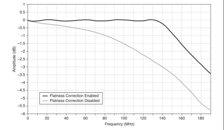
Figure 2. Main Path Filter Enabled Amplitude Response with Flatness Correction
Enabled and Disabled, 400 MS/s, Gain=2.5, Differential, Referenced to 50 kHz, Representative Unit
Figure 3. Direct Path Amplitude Response with Flatness Correction Enabled and
Disabled, 400 MS/s, Differential, Referenced to 50 kHz, Representative Unit
– 80 – 100– – 120– – 140– – 160– – 180– – Frequency (MHz) –6 –5.5 –5 –4.5 –3.5 –4 –3 –2 –2.5 –1.5 –1 –0.5 0 1 0.5 0 20 40 60 80 100 120 140 160 180 Amplitude (dB) Frequency (MHz) Flatness Correction Enabled
Flatness Correction Disabled
– 80 – 100– – 120– – 140– – 160– – 180– – Frequency (MHz) – – –6 – –5.5 – –5 – –4.5 – –3.5 – –4 – –3 – –2 – –2.5 – –1.5 – –1 – –0.5 – 0 – 1 – 0.5 0 – 20– – 40– – 60– – 80– – 100– – 120– – 140– – 160– – 180– – Amplitude (dB) Frequency (MHz) Flatness Correction Enabled
Figure 4. Main and Direct Path Amplitude Response with Flatness Correction Enabled,
400 MS/s, Differential, Referenced to 50 kHz, Representative Unit
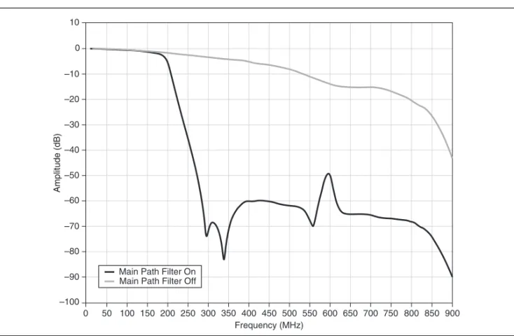
Figure 5. Main Path Characteristic Frequency Response of Image Suppression Filter,
Representative Unit – –0.25 – – –0.225 – –0.2 – –0.175 – –0.15 – –0.125 – –0.1 – –0.075 – –0.05 – –0.025 – 0 – 0.025 – 0.05 – 0.075 – 0.1 – 0.125 – 0.15 – 0.175 – 0.2 – 0.225 – 0.25 0 – 20– – 40– – 60– – 80– – 100– – 120– – 140– – 160– – 180– – Amplitude (dB) Frequency (MHz) Direct Path Main Path 0 50 100 150 200 250 300 350 400 450 500 550 600 650 700 750 800 850 900 Frequency (MHz) –90 –100 –80 –60 –70 –50 –40 –30 –20 –10 0 10
Main Path Filter On Main Path Filter Off
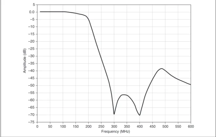
Figure 6. Direct Path Characteristic Frequency Response of Image Suppression Filter,
Representative Unit
Note Sinc response due to DAC sampling is not included in Figure 5 or Figure 6.
– 0 50– 100– 150– 200– 250– 300– 350– 400– 450– 500– 550– 600– Frequency (MHz) Amplitude (dB) – –75 – –70 – –65 – –60 – –55 – –50 – –45 – –40 – –35 – –30 – –25 – –20 – –15 – –10 – –5 – 0.0 – 5
Spe ci fic ation Va lu e Comment s
Spectral Characteristics Spurious Fr
ee Dynamic Range (SFDR) a t 1M H z SF D R (dB) Nomi na l. 400 MS/s, amplitude –1 dBFS. Includes alia sed harmonics. Di ff ere n ti al output me as ured
single- ended with a balun
or di ff ere n tia l am p. T ermin ate d in to 50 Ω to grou nd on ea ch te rm inal . Fr equenc y Range Sing le-Ended Main P ath Di ff ere n ti al Main P ath Dif fer ent ial Dir ect P ath Gain = 0.25 0.5 VPPSE Gain = 0.625 1.2 5 VPPS E Gain = 1.25 2. 5 VP PSE Gain = 0.5 , 1V PP D Gain = 1.25, 2. 5 VPP D Gain = 2.5, 5V PP D Gain = 0.5, 1V PPD SFDR with Harmonics DC to 7 MHz 82 85 88 DC to 200 MHz 75 75 75 SFDR without Harmonics DC to 7 MHz 82 88 95 98 98 DC to 200 MHz 82 83 84 84 84
S p eci fic a tion Va lu e Comment s Spectral Cha racte ristics (Continue d) SF DR with Harmonics SF D R ( d B) 40 0 MS/s, amplitu de –1 dBFS. Measured from DC to 20 0 M Hz. Al l v alue s ar e typ ica l and include alia se d harmo nics. Di ff er en tia l ou tput me as ure d sing le-ended with balun. Termi n at ed into 50 Ω to gr ound o n ea ch te rmi n al . Frequenc y Single-Ended Main P ath Dif fe rent ial Ma in P ath Di ff ere n ti al Direct P ath Gain = 0. 25, 0.5 VP PSE Gain = 0.625 , 1.25 VPPS E Gain = 1.25, 2.5 VPPS E Gain = 0.5, 1V PP D Gain = 1.25 , 2. 5 VPP D Gain = 2.5, 5V PPD Gain = 0.5, 1V PPD 10 MHz 73 ( 7 5) * 73 (75) * 73 (75) * 7 3 (75) * 73 ( 75) * 73 (73) * 73 (75) * 60 MHz 65 61 56 69 67 64 70 (72) * 100 MHz 53 52 49 55 54 53 60 120 MHz 62 62 62 62 62 62 62 160 MHz — 62 Note : The fi rs t specif ication listed is f o r a 10.0 M H z sinus oid at a 400 MS/s sample r ate (w av ef or m contains 40 unique sample s) , a n d the sp ecif ica tion in par entheses is for a 1 0 .0 MHz s inu so id a t a 39 9. 9 MS/s s am p le r ate ( w av efo rm c o n tain s o v er 3 0 0 0 un iq ue s am p les with un iq ue D A C co des ). * Lo ng , no nr ep etiti v e w av ef o rm s lik e m odu lated s ignals of fe r better sp ur ious p er fo rm ance. F o r per iodic w av efo rms r epr esented by a small num ber o f un ique samples, D A C nonlinear
ities limit dynamic specif
Specification Value Comments Spectral Characteristics (Continued)
SFDR without Harmonics Frequency SFDR (dB) 400 MS/s sample rate. Amplitude –1 dBFS. Measured from DC to 200 MHz. All values are typical and include aliased harmonics. Differential output measured single-ended with balun. Characterized at the same gain ranges as
SFDR with Harmonics. Single-Ended and Differential Main Path Differential Direct Path 10 MHz 74 (76)* 74 (76)* 60 MHz 72 (74)* 72 (74)* 100 MHz 66 64 120 MHz 62 62 160 MHz — 62
Note: The first specification listed is for a 10.0 MHz sinusoid at a 400 MS/s sample rate (waveform contains 40 unique samples), and the specification in parentheses is for a 10.0 MHz sinusoid at a 399.9 MS/s sample rate (waveform contains over 3000 unique samples with unique DAC codes).
* Long, nonrepetitive waveforms, like modulated signals, offer better spurious performance. For periodic waveforms
Specification Value Comments Spectral Characteristics (Continued)
Out-of-Band Performance
In-Band Tone Frequency (MHz)
Out-of-Band Spur Level (dBm) Nominal. Generating full-scale sine wave at frequency listed, 400 MS/s. Measured 200 MHz to 2 GHz. Anti-imaging filter is fixed and optimized for 400 MS/s. Main Path, Filter Enabled
0 to 20 <–65 dBm 20 to 50 <–45 dBm Direct Path 0 to 20 <–80 dBm 20 to 50 <–65 dBm Channel-to- Channel Crosstalk Aggressor Output
Amplitude Main Path*
Measured single ended at the victim channel, 0 V DC output, 400 MS/s sample rate. Aggressor channel is terminated into 50Ω, sine wave output, 400 MS/s sample rate. All values nominal. 2.5 –90 dBc, 0 MHz to 200 MHz 1.25 –85 dBc, 0 MHz to 200 MHz 0.5 –80 dBc, 0 MHz to 200 MHz 0.15 –70 dBc, 0 MHz to 200 MHz Direct Path <80 dBc, 0 MHz to 200 MHz <90 dBc, 0 MHz to 150 MHz
* The dBc values are referenced to the differential tone power on the aggressor channel. Results are independent of victim
Specification Value Comments Spectral Characteristics (Continued)
Total Harmonic Distortion (THD)
Main Path Amplitude
–1 dBFS. Includes the 2nd through the
6th harmonic.
All values are typical. Measured at 0.1 MHz offset. 400 MS/s sample rate. Differential Main path output measured single ended with a balun. Output Amplitude Frequency (MHz) THD (dBc) Single-Ended Differential 2.5 VPPSE, 5 VPPD 10 –71 –71 20 –66 –69 40 –59 –64 60 –55 –61 80 –51 –55 120 –50 –51 140 –50 –52 160 –50 –53 1.25 VPPSE, 2.5 VPPD 10 –78 –75 20 –72 –73 40 –63 –69 60 –60 –65 80 –56 –59 120 –56 –59 140 –56 –59 160 –55 –59 0.5 VPPSE, 1 VPPD 10 –80 –79 20 –74 –75 40 –68 –69 60 –64 –69 80 –62 –65 120 –65 –70 140 –64 –69 160 –61 –66
Spectral Characteristics (Continued) Total Harmonic
Distortion (THD)
Direct Path Amplitude
–1 dBFS. Includes the 2nd through the
6th harmonic.
All values are typical. Measured at 0.1 MHz offset. 400 MS/s sample rate. Differential Direct path output measured single ended with a balun. Output Amplitude Frequency (MHz) THD (dBc) 0.5 VPPSE, 1 VPPD 10 –75 20 –70 40 –68 80 –68 100 –68 120 –78 160 –83
Spectral Characteristics (Continued) Intermodulation
Distortion (IMD3)
Single-Ended and Differential Main Path The waveform amplitude for each tone is –7 dBFS. Typical. 400 MS/s sample rate. Two-tone frequencies are frequency ±100 kHz. Output Amplitude Frequency (MHz) IMD (dBc) 2.5 VPPSE, 5 VPPD 10 –87 20 –82 40 –71 60 –63 80 –57 120 –51 160 –48 1.25 VPPSE, 2.5 VPPD 10 –92 20 –87 40 –79 60 –72 80 –66 120 –61 160 –57 0.5 VPPSE, 1 VPPD 10 –87 20 –85 40 –82 60 –79 80 –75 120 –79 160 –75
Spectral Characteristics (Continued) Intermodulation
Distortion (IMD3)
Single-Ended and Differential Main Path The digital amplitude for each tone is –7 dBFS. All values are typical. 400 MS/s sample rate. Two-tone frequencies are frequency ±100 kHz. Differential Direct path output measured single-ended with balun. Output Amplitude Frequency (MHz) IMD (dBc) 0.1 VPPSE, 0.2 VPPD 10 –89 20 –83 40 –78 60 –73 80 –69 120 –66 160 –65 Direct Path Output Amplitude Frequency (MHz) IMD (dBc) 0.5 VPPSE, 1 VPPD 10 –84 20 –81 40 –75 80 –71 100 –68 120 –68 160 –66
Specification Value Comments Spectral Characteristics (Continued)
Average Noise Density Output Amplitude Average Noise Density Average noise density from DC to 200 MHz generating –40 dBFS, 1 MHz sine wave at 400 MS/s. Differential output measured with a balun. Differential dBm numbers referred back to a 50 Ω system. Single-Ended Main Path
VPPSE dBm dBm/Hz dBFS/Hz
2.5 12 12.57 –145 –157
0.5 –2 9.99 –147 –145
0.06 –20.4 9.99 –147 –126.6
Differential Main Path
VPPD dBm dBm/Hz dBFS/Hz
5 18 17.76 –142 –160
1 4 14.11 –144 –148
0.12 –14.4 14.11 –144 –129.6
Differential Direct Path
VPPD dBm dBm/Hz dBFS/Hz 1 4.0 2.24 –160 –164 nV Hz ---nV Hz ---nV Hz
---Figure 7. Single-Ended Main Path, Total Harmonic Distortion, Typical
Figure 8. Differential Main Path, Total Harmonic Distortion, Typical
Total Harmonic Distortion (dBc)
–48 –46 –82 –84 –80 –78 –76 –74 –70 –68 –66 –64 –62 –60 –58 –54 –52 –56 –50 Frequency (MHz) 175 150 0 25 50 75 100 125 Gain: 2.50 Gain: 1.25 Gain: 0.50
Total Harmonic Distortion (dBc)
–48 –46 –82 –84 –80 –78 –76 –74 –72 –70 –68 –66 –64 –62 –60 –58 –54 –52 –56 –50 Frequency (MHz) 175 150 0 25 50 75 100 125 Gain: 2.50 Gain: 1.25 Gain: 0.50
Figure 9. Direct Path, Total Harmonic Distortion, Typical
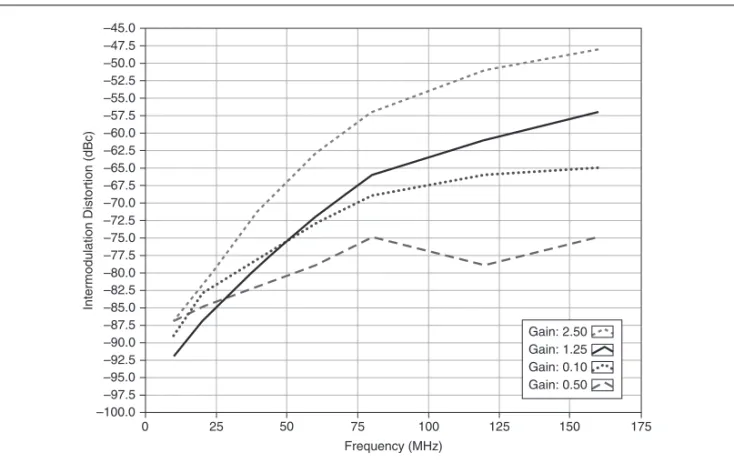
Figure 10. Single-Ended and Differential Main Path, Intermodulation Distortion,
200 kHz Separation, Typical
–
0.0 20– 40– 60– 80– 100– Frequency (MHz)
Total Harmonic Distortion (dBc)
– 120 140– 160– 180– 200– – – – – – – – – – – – – –90 –85 –80 –75 –70 –65 –60 –55 –50 –45 –40 –35 –30 Intermodulation Distortion (dBc) –47.5 –45.0 –92.5 –95.0 –90.0 –87.5 –85.0 –82.5 –80.0 –77.5 –75.0 –72.5 –70.0 –67.5 –65.0 –62.5 –60.0 –55.0 –52.5 –57.5 –50.0 Frequency (MHz) 175 150 0 25 50 75 100 125 –97.5 –100.0 Gain: 1.25 Gain: 0.10 Gain: 0.50 Gain: 2.50
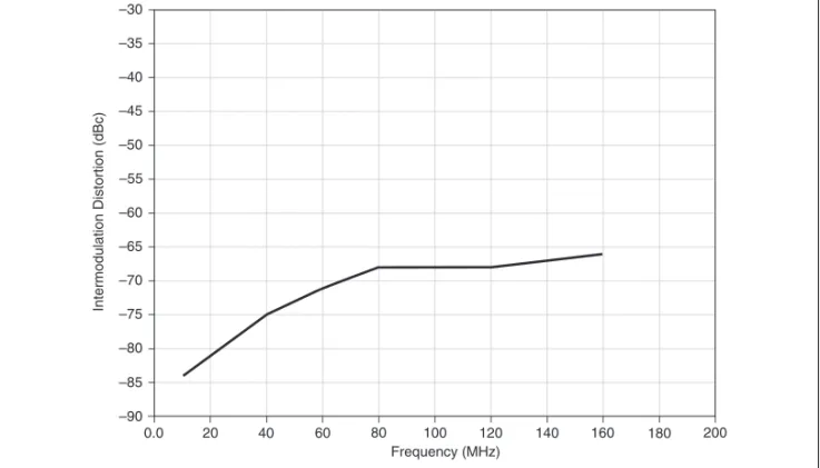
Figure 11. Direct Path, Intermodulation Distortion, 200 kHz Separation, Typical
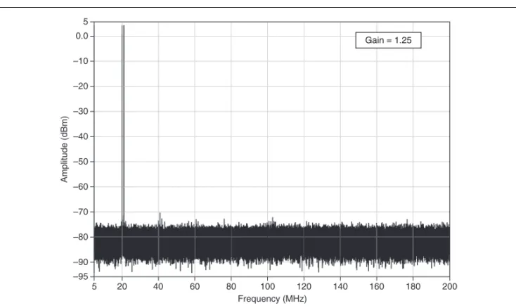
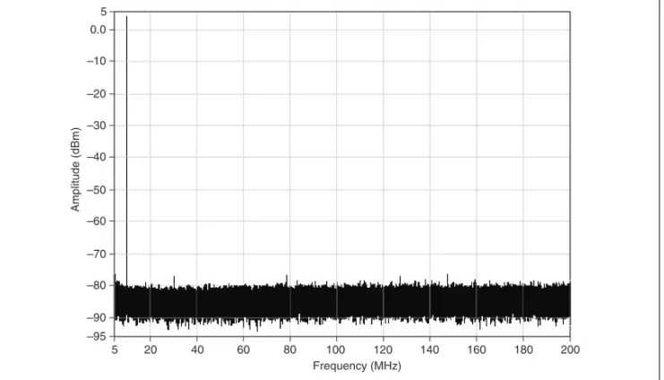
Figure 12. Single-Ended Main Path 10.000 MHz Single-Tone Spectrum, 400 MS/s,
–1 dBFS, Representative Unit – 0.0 20– 40– 60– 80– 100– 120– 140– 160– 180– 200– Frequency (MHz) Intermodulation Distortion (dBc) – –90 – –85 – –80 – –75 – –70 – –65 – –60 – –55 – –50 – –45 – –40 – –35 – –30 Amplitude (dBm) Frequency (MHz) 5 20 40 60 80 100 120 140 160 180 200 10 0 –10 –20 –30 –40 –50 –60 –70 –80 –90 Gain = 1.25 Gain = 1.25
Figure 13. Single-Ended Main Path 10.100 MHz Single-Tone Spectrum, 400 MS/s,
–1 dBFS, Representative Unit
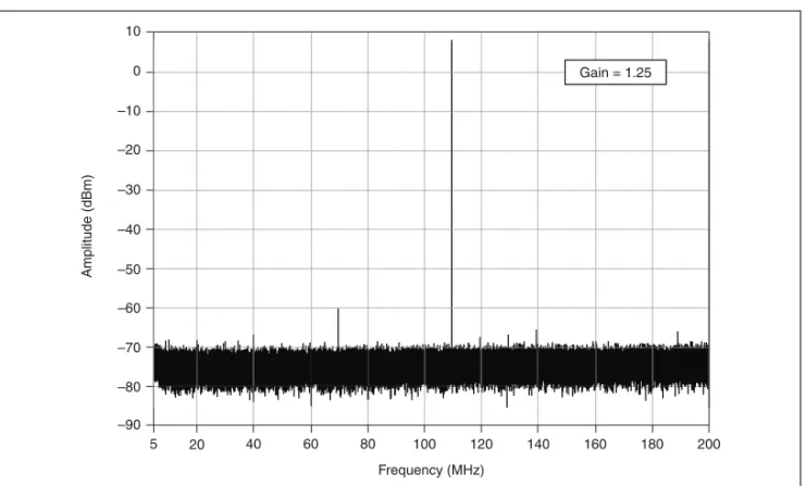
Figure 14. Single-Ended Main Path 110.100 MHz Single-Tone Spectrum, 400 MS/s,
–1 dBFS, Representative Unit Amplitude (dBm) Frequency (MHz) 5 20 40 60 8 100 120 140 160 180 200 10 0 –10 –20 –30 –40 –50 –60 –70 –80 –90 Gain = 1.25 Gain = 1.25 Amplitude (dBm) Frequency (MHz) 5 20 40 60 80 100 120 140 160 180 200 10 0 –10 –20 –30 –40 –50 –60 –70 –80 –90 Gain = 1.25 Gain = 1.25
Figure 15. Differential Main Path 10.000 MHz Single-Tone Spectrum, 400 MS/s,
–1 dBFS, Measured Through Balun, Representative Unit
Figure 16. Single-Ended Main Path Intermodulation Distortion, 1 MHz Separation,
20 MHz Tone, 400 MS/s, –7 dBFS, Representative Unit
Amplitude (dBm) Frequency (MHz) 5 20 40 60 80 100 120 140 160 180 10 15 0 –10 –20 –30 –40 –50 –60 –70 –80 –90 Gain = 1.25 Gain = 1.25 5 20 40 60 80 100 120 140 160 180 200 –90 –95 –80 –70 –60 –50 –40 –30 –20 –10 0.0 5 Frequency (MHz) Amplitude (dBm) Gain = 1.25
Figure 17. Direct Path Intermodulation Distortion, 1 MHz Separation,
20 MHz Tone, 400 MS/s, –7 dBFS, Representative Unit
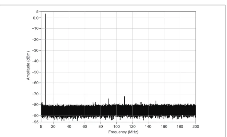
Figure 18. Direct Path 10.000 MHz Single-Tone Spectrum, 400 MS/s, –1 dBFS, Representative Unit – 5 20– 40– 60– 80– 100– 120– 140– 160– 180– 200– Frequency (MHz) Amplitude (dBm) – –95 – –90 – –80 – –70 – –60 – –50 – –40 – –30 – –20 – –10 – 0.0 – – – – – – – – – – – – – – – – – – – – – – 5 20– 40– 60– 80– 100– 120– 140– 160– 180– 200– Frequency (MHz) Amplitude (dBm) – –95 – –90 – –80 – –70 – –60 – –50 – –40 – –30 – –20 – –10 – 0.0 – 5 – 5 20– 40– 60– 80– 100– 120– 140– 160– 180– 200– Frequency (MHz) Amplitude (dBm ) – –– –95 – –90 – – –80 – –70 – –60 – –50 – –40 – –30 – –20 – –10 – 0.0 – 5
Figure 19. Direct Path 10.100 MHz Single-Tone Spectrum, 400 MS/s, –1 dBFS, Representative Unit
Note The noise floor on all spectral graphs is limited by the measurement device.
– 5 20– 40– 60– 80– 100– 120– 140– 160– 180– 200– Frequency (MHz) Amplitude (dBm) – –95 – –90 – –80 – –70 – –60 – –50 – –40 – –30 – –20 – –10 – 0.0 – 5 – 5 20– 40– 60– 80– 100– 120– 140– 160– 180– 200– Frequency (MHz) Amplitude (dBm ) – –95 – – –90 – – –80 – –70 – –60 – –50 – –40 – –30 – –20 – –10 – 0.0 – 5
Specification Value Comments Output Phase Noise and Jitter*
Sample Clock Source Output Freq. (MHz)
System Phase Noise Density† (dBc/Hz) System
Output Integrated Jitter† — 100 Hz 1 kHz 10 kHz 100 kHz 1 MHz Internal, High-Resolution Clock, 400 MS/s 10 <–121 <–137 <–146 <–152 <–153 <350 fs Typical. 100 <–101 <–119 <–126 <–136 <–141 <350 fs CLK IN External 10 MHz Reference Clock, 400 MS/s 10 <–122 <–135 <–146 <–152 <–153 <350 fs Typical. 100 <–105 <–115 <–126 <–136 <–141 <350 fs
Note: Specifications valid for both main path and direct path, limited by the output noise floor.
* Generating sine wave at an output frequency of 400 MS/s.
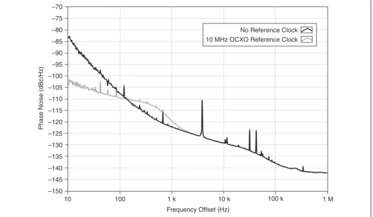
Figure 20. Phase Noise on a Representative Module, 100 MHz Sine Wave,
400 MS/s Internal Clock Sample Rate, Chassis Fans Low, Shown With and Without a Reference Clock
Figure 21. Phase Noise on a Representative Module, 100 MHz Sine Wave,
400 MS/s Internal Clock Sample Rate, Chassis Fans High, No Reference Clock
–70 –150 –145 –140 –135 –130 –125 –120 –115 –110 –105 –100 –95 –90 –85 –80 –75 1 M 10 100 1 k 10 k 100 k Phase Noise (dBc/Hz) Frequency Offset (Hz) No Reference Clock 10 MHz OCXO Reference Clock
Phase Noise (dBc/Hz) –70 –150 –145 –140 –135 –130 –125 –120 –115 –110 –105 –100 –95 –90 –85 –80 –75 Frequency Offset (Hz) 1M 10 100 1k 10k 100k No Reference Clock
Specification Value Comments Suggested Maximum Frequencies for Common Functions
Function Main Path Direct Path The Direct
path is optimized for frequency-domain performance. Sine 135 MHz 145 MHz Square 150 MHz* 33 MHz (<133 V/μs slew rate)†
Ramp 20 MHz* 1 MHz (<50 V/μs slew rate)†
Triangle 20 MHz*(5 MHz) 8 MHz
Pulse Response Rise/Fall Time (10% to 90%)
Flatness Correction Disabled Flatness Correction Enabled Typical. Values into 50Ω at each output. Main Path, Filter Disabled
1.5 ns —
Main Path, Filter Enabled
3 ns 3 ns
Direct Path
3 ns 2.5 ns
Aberration Flatness Correction Disabled Flatness Correction Enabled Typical. Values into 50Ω at each output. Main Path, Filter Disabled
3% —
Main Path, Filter Enabled†
18% 25%
Direct Path*
18% (7%)‡ 22%
* Filter disabled.
† Aberrations on pulsed waveforms are due to the analog reconstruction filter and can be significantly reduced if waveform
data has limited slew rate. Waveforms with higher slew rates are not recommended.
‡ 7% aberrations achievable with 133 V/μs slew rate limiting on waveform data. Pulsed waveforms should contain multiple
Clocking
The NI 5451 offers many clocking options. Waveform generation is driven by the Sample clock. You have multiple choices for configuring the device clocking, as shown in the following figure.
Figure 22. NI PXIe-5451 Clocking
Tip Refer to the clocking documentation in the NI Signal Generators Help by navigating to NI Signal Generators Help»Devices»NI 5451»Theory of Operation»Clocking for more information about NI 5451 clocking options.
Onboard Sample Clock
The following figure shows the NI 5451 onboard Sample clock path.
Figure 23. NI PXIe-5451 Onboard Sample Clock and External Reference Clock Path
PXI_CLK10 CLK IN High- Resolution Oscillator PLL CLK OUT (None) Divide/M Sample Clock Timebase/M Multiply * W and Phase Adjust Divide/N Sample Clock Timebase Channel Delay Channel Delay CH 0 Sample Clock CH 1 Sample Clock Divide/K Reference Clock
External Sample Clock
External Sample Clock Timebase
PXI_CLK10 CLK IN High- Resolution Oscillator PLL CLK OUT (None) Divide/M Sample Clock Timebase/M Multiply * W and Phase
Adjust Sample Divide/N
Clock Timebase Channel Delay Channel Delay CH 0 Sample Clock CH 1 Sample Clock Divide/K Reference Clock
External Sample Clock
Specification Value Comments Sample Clock Rate Range 12.2 kS/s to 400 MS/s — Sample Clock Rate Frequency Resolution <5.7 μHz Varies with Sample clock frequency. Specification is worst-case. Sample Clock Delay
0 ns to 2 ns, independent per channel Set in software with the Channel Delay property or the NIFGEN_ATTR_ CHANNEL_DELAY attribute. Sample Clock Delay Resolution 10 ps Nominal. Sample Clock Timebase Phase Adjust
±1 Sample clock timebase period —
Reference Clock Sources
1. None (internal reference) 2. PXI_CLK10 (backplane) 3. CLK IN (front panel connector)
External Sample Clock
The following figure shows the NI 5451 external Sample clock path.
Figure 24. NI PXIe-5451 External Sample Clock Path
Reference Clock Frequency 1 MHz to 100 MHz in increments of 1 MHz 100 MHz to 200 MHz in increments of 2 MHz 200 MHz to 400 MHz in increments of 4 MHz Default of 10 MHz. ±0.01% accuracy required Internal Reference Clock Frequency Accuracy ±0.01% Measured without an external Reference clock. When locking to a Reference clock, frequency accuracy is solely dependent on the frequency accuracy of the Reference clock source.
Specification Value Comments
PXI_CLK10 CLK IN High- Resolution Oscillator PLL CLK OUT (None) Divide/M Sample Clock Timebase/M Multiply * W and Phase
Adjust Sample Divide/N
Clock Timebase Channel Delay Channel Delay CH 0 Sample Clock CH 1 Sample Clock Divide/K Reference Clock
External Sample Clock
Specification Value Comments External
Sample Clock Source
CLK IN, front panel connector, with multiplication and division — External Sample Clock Rate 10 MS/s, 20 MS/s to 400 MS/s — Sample Clock Rate Range 12.2 kS/s to 400 MS/s — Multiplication/ Division Factor Range
Varies depending on the external Sample clock rate Shown as
Multiply*W and Divide/N in
Figure 24. Sample Clock
Delay
0 ns to 2 ns, independent per channel Set in software with the Channel Delay property or the NIFGEN_ATTR_ CHANNEL_DELAY attribute. Sample Clock Delay Resolution 10 ps Nominal. Sample Clock Timebase Phase Adjust
External Sample Clock Timebase
The following figure shows the NI 5451 external Sample clock timebase path.
Figure 25. NI PXIe-5451 External Sample Clock Timebase Path
Specification Value Comments
External Sample Clock Timebase Sources
CLK IN, front panel connector, with division —
External Sample Clock Timebase Rate Range 200 MS/s to 400 MS/s — Divide Factor Range 1, 2 to 32768 in steps of 2 Shown as Divide/N in Figure 25. Sample Clock Delay
0 ns to 2 ns, independent per channel —
Sample Clock Delay Resolution 10 ps Nominal. PXI_CLK10 CLK IN High- Resolution Oscillator PLL CLK OUT (None) Divide/M Sample Clock Timebase/M Multiply * W and Phase
Adjust Sample Divide/N
Clock Timebase Channel Delay Channel Delay CH 0 Sample Clock CH 1 Sample Clock Divide/K Reference Clock
External Sample Clock
Exporting Clocks
Terminals
CLK IN
(Sample Clock and Reference Clock Input, Front Panel Connector)
Specification Value Comments
Destination Rates
Reference Clock
CLK OUT 1 MHz to 400 MHz —
PFI<0..1> 1 MHz to 200 MHz
Sample Clock CLK OUT 100 kHz to 400 MHz With optional
divider. PFI<0..1> 0 MHz to 200 MHz
Sample Clock Timebase
CLK OUT 100 kHz to 400 MHz With optional
divider. PFI<0..1> 0 MHz to 200 MHz
Specification Value Comments
Direction Input —
Destinations 1. Reference clock 2. Sample clock
3. Sample clock timebase
— Frequency Range 1 MHz to 400 MHz Not applicable for all destinations. Refer to the specifications for your clocking configuration for applicable ranges. Input Voltage Range 500 mVpk-pk to 5 Vpk-pk into 50 Ω (–2 dBm to +18 dBm) 50% duty cycle input. 550 mVpk-pk to 4.5 Vpk-pk into 50 Ω (–1.2 dBm to +17 dBm) 45% to 55% duty cycle input.
CLK OUT
(Sample Clock and Reference Clock Output, Front Panel Connector)
Input Protection Range 6 Vpk-pk into 50 Ω 19.5 dBm 50% duty cycle input. 5.4 Vpk-pk into 50 Ω 18.5 dBm 45% to 55% duty cycle input. Duty Cycle Requirements 45% to 55% — Input Impedance 50 Ω, nominal — Input Coupling AC — Voltage Standing Wave Ratio (VSWR) 1.3:1 up to 2 GHz Nominal.Specification Value Comments
Direction Output —
Sources 1. Sample clock, divided by integer K (1≤ K ≤ 3, minimum) 2. Reference clock
3. Sample clock timebase, divided by integer M (1 ≤ M ≤ 1048576) The maximum value of the divisor, K, is sample rate dependent. Frequency Range 100 kHz to 400 MHz —
Output Voltage ≥0.7 Vpk-pk into 50 Ω Typical.
Maximum Output Overload 3.3 Vpk-pk from a 50 Ω source — Output Coupling AC — VSWR 1.3:1 up to 2 GHz Nominal.
PFI 0 and PFI 1
(Programmable Function Interface, Front Panel Connectors)
Specification Value Comments
Direction Bidirectional —
Frequency Range
DC to 200 MHz —
As an Input (Trigger)
Destinations Start trigger, Script trigger —
Input Range 0 V to 5 V — Input Protection Range –2 V to +6.5 V — VIH 1.8 V — VIL 1.5 V — Input Impedance 10 kΩ, nominal —
As an Output (Event)
Sources 1. Sample clock divided by integer K (2 ≤ K ≤ 3, minimum) 2. Sample clock timebase divided by integer M
(2 ≤ M ≤ 1048576) 3. Reference clock 4. Marker event 5. Data marker event 6. Exported Start trigger 7. Exported Script trigger 8. Ready for Start event 9. Started event 10. Done event The maximum value of the Sample clock divisor, K, is sample rate dependent. Output Impedance
Main Path Direct Path
50 Ω, nominal 50 Ω (+4%, –0%)
Maximum Output Overload
–2 V to +6.5 V —
VOH Minimum: 2.4 V (open load), 1.3 V (50 Ω load) Output drivers
are +3.3 V TTL/CMOS compatible up to 200 MHz. VOL Maximum: 0.4 V (open load), 0.2 V (50 Ω load)
Rise/Fall Time 3 ns Typical.
Load of 10 pF.
Triggers and Events
Triggers
Specification Value Comments
Sources 1. PFI<0..1> (SMB front panel connectors) 2. PXI_Trig<0..7> (backplane connector)
3. Immediate (does not wait for a trigger). Default.
—
Types 1. Start trigger edge
2. Script trigger edge and level 3. Software trigger
—
Edge Detection Rising, falling —
Minimum Pulse Width 25 ns Refer to the ts1 documentation in the NI Signal Generators Help by navigating to NI Signal Generators Help»Devices» NI 5451» Triggering» Trigger Timing. Delay from Trigger to Analog Output with OSP Disabled
154 Sample clock timebase periods + 65 ns, nominal Refer to the ts2 documentation in the NI Signal Generators Help by navigating to NI Signal Generators Help»Devices» NI 5451» Triggering» Trigger Timing. Additional Delay with OSP Enabled
Trigger Exporting Exported
Trigger Destinations
1. PFI<0..1> (SMB front panel connectors) 2. PXI_Trig<0..6> (backplane connector)
—
Exported Trigger Delay
50 ns, nominal Refer to the ts3
documentation in the NI Signal Generators Help by navigating to NI Signal Generators Help»Devices» NI 5451» Triggering» Trigger Timing. Exported Trigger Pulse Width >150 ns Refer to the ts4 documentation in the NI Signal Generators Help by navigating to NI Signal Generators Help»Devices» NI 5451» Triggering» Trigger Timing.
Events
Specification Value Comments
Destinations 1. PFI<0..1> (SMB front panel connectors) 2. PXI_Trig<0..6> (backplane connector)
—
Types Marker<0..3>, Data Marker<0..1>, Ready for Start, Started, Done
There are two data markers per channel. Quantum Marker position must be placed at an integer multiple of
two samples.
—
Width Adjustable, minimum of 2 samples Default is 150 ns. Refer to the tm2 documentation in the NI Signal Generators Help by navigating to NI Signal Generators Help» Fundamentals» Waveform Fundamentals» Events» Marker Events. Skew Destination With Respect to Analog Output Refer to the tm1 documentation in the NI Signal Generators Help by navigating to NI Signal Generators Help» Fundamentals» Waveform Fundamentals» Events» Marker Events. PFI<0..1> ±3 Sample clock periods
Waveform Generation Capabilities
Specification Value Comments
Memory Usage
The NI 5451 uses the Synchronization and Memory Core (SMC) technology in which waveforms and instructions share onboard memory. Parameters, such as number of segments in sequence list, maximum number of waveforms in memory, and number of samples available for waveform storage, are flexible and user defined.
For more information, refer to the NI Signal Generators Help by navigating to NI Signal Generators Help» Programming» Reference» NI-TClk Synchronization Help. Onboard Memory Size
128 MB option 512 MB option 2 GB option
Memory is shared between both channels. 134,217,728 bytes 536,870,912 bytes 2,147,483,648 bytes Loop Count 1 to 16,777,215
Burst trigger: Unlimited
—
Quantum Waveform size must be an integer multiple of two samples. — Output Modes
Arbitrary Waveform mode
A single waveform is selected from the set of waveforms stored in onboard memory and generated.
—
Script mode A script allows you to link and loop multiple waveforms in complex combinations. A script is a series of instructions that indicates how waveforms saved in the onboard memory should be sent to the device. The script can specify the order in which the waveforms are generated, the number of times they are generated, and the triggers and markers associated with the generation.
Output Modes (Continued) Arbitrary
Sequence mode
A sequence directs the NI 5451 to generate a set of waveforms in a specific order. Elements of the sequence are referred to as segments. Each segment is associated with a set of instructions. The instructions identify which waveform is selected from the set of waveforms in memory, how many loops (iterations) of the waveform are generated, and at which sample in the waveform a marker output signal is sent.
—
Minimum Waveform Size (Samples)
Trigger Mode Number of Channels Arbitrary Waveform Mode Arbitrary Sequence Mode >180 MS/s Arbitrary Sequence Mode ≤180MS/s The minimum waveform size is sample rate dependent. Measured using a 200 MHz trigger. Single 1 4 2 2 2 4 4 4 Continuous 1 142 140 58 2 284 280 116 Stepped 1 210 154 54 2 420 308 108 Burst 1 142 1,134 476 2 284 2,312 952
Memory Limits (Bytes) Number of Channels 128 MB 512 MB 2 GB Arbitrary Waveform Mode, Maximum Waveform Memory 1 67,108,352 268,434,944 1,073,741,312 All trigger modes except where noted. 2 33,553,920 134,217,216 536,870,400 Arbitrary Sequence Mode, Maximum Waveform Memory 1 67,108,352 268,434,944 1,073,741,312 Condition: One or two segments in a sequence. 2 33,553,920 134,217,216 536,870,400 Arbitrary Sequence Mode, Maximum Waveforms 1 1,048,575 4,194,303 16,777,217 Condition: One or two segments in a sequence. 2 524,287 2,097,151 8,388,607 Arbitrary Sequence Mode, Maximum Segments in a Sequence 1 8,388,597 33,554,421 134,217,717 Condition: Waveform size is <4,000 samples. 2 4,194,293 16,777,205 67,108,853
Onboard Signal Processing
Figure 26. Onboard Signal Processing Block Diagram Waveform Play Times
Maximum Play Time, Sample Rate Number of Channels 128 MB 512 MB 2 GB Single Trigger mode. Play times can be significantly extended by using Continuous, Stepped, or Burst Trigger modes.
400 MS/s 1 0.17 seconds 0.67 seconds 2.68 seconds
2 0.084 seconds 0.34 seconds 1.34 seconds
25 MS/s 1 2.68 seconds 10.74 seconds 42.95 seconds
2 1.34 seconds 5.37 seconds 21.47 seconds
100 kS/s 1 11 minutes 11 seconds 44 minutes 44 seconds 2 hours 58 minutes 57 seconds 2 5 minutes 35 seconds 22 minutes 22 seconds 1 hour 29 minutes 29 seconds
Specification Value Comments
Prefilter Gain I Prefilter Offset I Filtering and Interpolation I Onboard Signal Processing
Digital Gain DAC 0 Output Engine Waveform Memory Prefilter Gain Q Prefilter Offset Q Filtering and Interpolation Q Digital Gain DAC 1 Programmable I/Q Gain & Offset Control
Pulse Shaping and Interpolation NCO-Based Frequency Translation and Upconversion I/Q Rate
Specification Value Comments I/Q Rate OSP Interpolation Range 2, 4, 8, 12, 16, 20 24 to 8,192 (multiples of 8) 8,192 to 16,384 (multiples of 16) 16,384 to 32,768 (multiples of 32) —
I/Q Rate (Sample clock rate) ÷ (OSP interpolation) Example: For a Sample clock rate of 400 MS/s, I/Q rate range = 12.2 kS/s to 200 MS/s. Data Processing Modes*
1. Real (I path only) 2. Complex (I/Q) — OSP Modes† 1. IF 2. Baseband — Maximum Bandwidth‡ 0.8 × I/Q rate —
Note: For more information about frequency translation and upconversion, refer to the NI Signal Generators Help and navigate to NI Signal Generators Help»Devices»NI 5451»Onboard Signal Processing (OSP)»Numerically Controlled Oscillator (NCO).
* Data Processing Mode describes the OSP engine data source. The data can be a single stream of real data (Real) or separate
streams of real and imaginary data (Complex).
† OSP Mode describes the signal processing function performed on the data after interpolation. In IF Mode, I and Q data
streams are quadrature upconverted to an intermediate frequency in a single output stream (to DAC 0/I). In Baseband Mode, frequency shifting can be applied to the I and Q data streams before they go into separate output streams (DAC 0/I and DAC 1/Q).
Prefilter Gain and Offset Prefilter Gain and Offset Resolution 21 bits — Prefilter Gain Range –16.0 to +16.0
(|Values| < 1 attenuate user data)
Unitless. Prefilter Offset Range –1.0 to +1.0 Applied after prefilter gain. Prefilter Output
(User data × Prefilter gain) + Prefilter offset Overflows occur when |Output| > 1. Finite Impulse Response (FIR) Filtering
Filter Types Parameter Minimum Maximum
Flat Passband 0.4 0.4 Lowpass filter that
minimizes ripple to
I/Q rate × Passband.
Raised Cosine Alpha 0.1 0.4 When using pulse
shaping, these filters require an OSP interpolation factor of 24 or greater. Root Raised Cosine Alpha 0.1 0.4
Numerically Controlled Oscillator (NCO) Maximum
Frequency
0.4 × sample rate —
Frequency Resolution
Sample rate/248 Example: 1.42μHz
with a sample rate of 400 MS/s.
Tuning Speed 250 μs Software- and
system-dependent.
Digital Performance Maximum NCO Spur <–90 dBc Full-scale output. Interpolating Flat Filter Passband Ripple <0.1 dB Passband from 0 to (0.4 × I/Q rate). Ripple is dependent upon the interpolation rate. Interpolating Flat Filter Out-of-Band Suppression >80 dB Stopband suppression
from (0.6 × I/Q rate).
Specif ication Va lu e Co mm en ts IF M odula ti on Perfo rma nce (N ominal) QA M Order Sy mb ol Ra te (MS /s) A lpha Bandw idt h E V M (%) MER (dB) — 40 MH z IF 70 MHz IF 11 0 MHz IF 40 MH z IF 70 MH z IF 1 10 MH z IF M = 4 0. 16 0.25 200 k H z 0. 2 0.2 0.2 57 57 56 0. 80 0.25 1.00 MHz 0. 2 0.2 0.2 57 56 55 4. 09 0.22 4.98 MHz 0. 2 0.3 0.2 57 52 55 M = 16 17 .6 * 0.25 22.0 MHz 0. 3 0.5 0.4 51 45 49 32 .0 * 0.25 40.0 MHz 0. 6 — 0.6 42 — 43 M = 64 5. 36 0.15 6.16 MHz 0. 2 0.3 0.2 54 51 53 6. 95 0.15 7.99 MHz 0. 3 0.3 0.3 52 51 50 25 .0 0.15 28 .75 M H z 0. 4 0.6 0.4 46 43 46 M = 256 6. 95 0.15 7.99 MHz 0. 3 0.3 0.4 52 51 49 Note s: Sing le-E nd ed M ain path, –1 dB FS, Flatn ess Cor rectio n enab led , o nbo ar d Samp le clock witho u t ref er ence. Numb er of Sy mbo ls = 1, 0 24
All measurements were made using
the NI PX Ie -5 622 , not p h ase-lock ed to th e NI 5 451 , eq ualizatio n enab led , 40 MHz I F an d 1 10 MHz I F using inter n al clockin g , 70 MHz IF us ing e x ter n al clo ck ing at 100 M H z. * Fr actional interpola tion perf or med on data bef o re generati on. F o r mo re inf o rm ation ab out interpolation, ref er to the NI Sign al Gen erator s Help an d na v igate to NI Signal Generators Help»Devices»NI 5451»The o ry of Ope ration » Onboar d Signal Processing (O SP )»Baseband I n terpolation Considerations .
Calibration
Power
Specification Value Comments
External Calibration
The external calibration calibrates the ADC voltage reference and passband flatness. Appropriate constants are stored in nonvolatile memory.
—
Self-Calibration An onboard, 24-bit ADC and precision voltage reference are used to calibrate the DC gain and offset. Onboard channel alignment circuitry is used to calibrate the skew between channels. The self-calibration is initiated by the user through the software and takes approximately 60 seconds to complete. Appropriate constants are stored in nonvolatile memory.
—
Calibration Interval
Specifications valid within 1 year of external calibration —
Warm-up Time 15 minutes —
Specification Typical Maximum Comments
+3.3 VDC 1.9 A 2.0 A —
+12 VDC 2.6 A 2.9 A —
Software
Specification Value Comments
Driver Software
NI-FGEN is an IVI-compliant driver that allows you to configure, control, and calibrate the NI 5451. NI-FGEN provides application programming interfaces for many development environments.
—
Application Software
NI-FGEN provides programming interfaces for the following application development environments: • LabVIEW
• LabWindows™/CVI™
• Measurement Studio • Microsoft Visual C++ .NET • Microsoft Visual C/C++ • Microsoft Visual Basic
—
Interactive Control and Configuration Software
The FGEN Soft Front Panel supports interactive control of the NI 5451. The FGEN Soft Front Panel is included on the NI-FGEN DVD.
Measurement & Automation Explorer (MAX) provides interactive configuration and test tools for the NI 5451. MAX is also included on the NI-FGEN DVD.
You can use the NI 5451 with NI SignalExpress.
Physical
Hardware Front Panel
Figure 27. NI 5451 Front Panel
5 Vp-p MAX, 50 Ω LVT T L LVT T L 50 Ω 50 Ω 50 Ω 50 Ω CLK IN CLK OUT PF I 1 0.7 Vp-p NOM CH 1 + CH 0 – CH 0 + CH 1 – PF I 0 ESD SENSITIVE NI PXIe-5451
16-Bit 400 MS/s Arbitrary Waveform Generator
ACCESS ACTIVE
I +
Q + I –
Specification Value Comments Dimensions 3U, Two Slot, PXI Express module
21.6 cm × 4.0 cm × 13.0 cm (8.5 in. × 1.6 in. × 5.1 in.)
—
Weight 550 g (19.4 oz) —
Front Panel Connectors
Label Function(s) Connector Type —
CH 0+/I+ Differential and single-ended analog output
SMA
CH 0–/I– Differential analog output SMA
CH 1+/Q+ Differential and single-ended analog output
SMA
CH 1–/Q– Differential analog output SMA
CLK IN Sample clock, Sample clock timebase, and Reference clock input
SMA
CLK OUT Sample clock, Sample clock timebase, and Reference clock output
SMA
PFI 0 Marker output, trigger input, Sample clock output, exported trigger output
SMB
PFI 1 Marker output, trigger input, Sample clock output, exported trigger output
SMB
Front Panel LED Indicators
Label Function For more
information about the front panel LEDs, refer to the
NI Signal Generators Help.
ACCESS The ACCESS LED indicates the status of the PXI Express bus and the interface from the NI 5451 to the controller.
ACTIVE The ACTIVE LED indicates the status of the onboard generation hardware of the NI 5451.
NI PXIe-5451 Environment
Note To ensure that the NI PXIe-5451 cools effectively, follow the guidelines in the
Maintain Forced-Air Cooling Note to Users included in the NI 5451 kit. The NI PXIe-5451
is intended for indoor use only.
Specifications Value Comments
Operating Temperature
0 ºC to +55 ºC in all NI PXI Express chassis: Meets IEC 60068-2-1 and IEC 60068-2-2.
Note: Refer to KnowledgeBase 4AEB2ML1 at ni.com/kb for more information about maximizing PXI Express data transfer rates when operating at ambient temperatures below 10 ºC.
—
Storage Temperature
–25 ºC to +85 ºC. Meets IEC 60068-2-1 and IEC 60068-2-2. —
Operating Relative Humidity
10% to 90%, noncondensing. Meets IEC 60068-2-56. —
Storage Relative Humidity
5% to 95%, noncondensing. Meets IEC 60068-2-56. —
Operating Shock
30 g, half-sine, 11 ms pulse. Meets IEC 60068-2-27. Test profile developed in accordance with MIL-PRF-28800F.
Spectral and jitter specifications could degrade. Storage
Shock
50 g, half-sine, 11 ms pulse. Meets IEC 60068-2-27. Test profile developed in accordance with MIL-PRF-28800F.
—
Operating Vibration
5 Hz to 500 Hz, 0.31 grms. Meets IEC 60068-2-64. Spectral and jitter
specifications could degrade. Storage
Vibration
5 Hz to 500 Hz, 2.46 grms. Meets IEC 60068-2-64. Test
profile exceeds requirements of MIL-PRF-28800F, Class B.
—
Altitude 2,000 meter maximum (at 25 °C ambient temperature) — Pollution
Degree
Compliance and Certifications
Safety
This product meets the requirements of the following standards of safety for electrical equipment for measurement, control, and laboratory use: • IEC 61010-1, EN 61010-1
• UL 61010-1, CSA 61010-1
Note For UL and other safety certifications, refer to the product label or the Online
Product Certification section.
Electromagnetic Compatibility
This product meets the requirements of the following EMC standards for electrical equipment for measurement, control, and laboratory use: • EN 61326-1 (IEC 61326-1): Class A emissions; Basic immunity • EN 55011 (CISPR 11): Group 1, Class A emissions
• AS/NZS CISPR 11: Group 1, Class A emissions • FCC 47 CFR Part 15B: Class A emissions • ICES-001: Class A emissions
Note For EMC declarations and certifications, refer to the Online Product Certification section.
CE Compliance
This product meets the essential requirements of applicable European Directives as follows:
• 2006/95/EC; Low-Voltage Directive (safety)
• 2004/108/EC; Electromagnetic Compatibility Directive (EMC)
Online Product Certification
To obtain product certifications and the Declaration of Conformity (DoC) for this product, visit ni.com/certification, search by model number or product line, and click the appropriate link in the Certification column.
Environmental Management
NI is committed to designing and manufacturing products in an environmentally responsible manner. NI recognizes that eliminating certain hazardous substances from our products is beneficial to the environment and to NI customers.
For additional environmental information, refer to the NI and the
Environment Web page at ni.com/environment. This page contains the environmental regulations and directives with which NI complies, as well as other environmental information not included in this document.
Waste Electrical and Electronic Equipment (WEEE)
EU Customers At the end of the product life cycle, all products must be sent to a WEEE recycling center. For more information about WEEE recycling centers, National Instruments WEEE initiatives, and compliance with WEEE Directive 2002/96/EC on Waste Electrical and Electronic Equipment, visit ni.com/environment/weee.⬉ᄤֵᙃѻક∵ᶧࠊㅵ⧚ࡲ⊩ ˄Ё
RoHS
˅
Ёᅶ᠋ National Instrumentsヺড়Ё⬉ᄤֵᙃѻકЁ䰤ࠊՓ⫼ᶤѯ᳝ᆇ⠽䋼ᣛҸ (RoHS)DŽ ݇ѢNational InstrumentsЁRoHSড়㾘ᗻֵᙃˈ䇋ⱏᔩ ni.com/environment/rohs_chinaDŽ (For information about China RoHS compliance, go to ni.com/environment/rohs_china.)