学位論文(要約)
Study on Two-dimensional
-Conjugated Pd and Pt Dithiolene Polymers
(パラジウムおよび白金の二次元π共役
ジチオレン錯体ポリマーの研究)
平成 28 年 7 月博士(理学)申請
東京大学大学院理学系研究科
化学専攻
PAL TIGMANSU
パル ティグマンスー
Abstract
The thesis describes the synthetic strategies of two-dimensional -conjugated heavier group 10 metal bis(dithiolene) complex nanosheets. I have demonstrated the synthetic problems for such system and the ways to overcome it in order to synthesize such multinuclear 2-D planar framework. In this study, interfacial synthesis of multi-layered films, control over redox potential of ligand, electro-catalytic properties of such films in hydrogen evolution reactions and conductivity were explored.
Chapter 1 deals with the brief introduction of 2-D architectures. I have discussed the importance, classifications and recent developments in the field of 2-D material science.
Chapter 2 deals with the synthetic strategies of the 2-D palladium bis(dithiolene) (PdDT) coordination nanosheets. The manipulation of the redox activity of the benzene hexathiol (BHT) ligand has been shown here by use of oxidizing agent. Pristine liquid-liquid interface was exploited for synthesis of thicker stacked coordination sheets; while going for thin layers of sheets, the gas-liquid interface was used. The structure, composition was comprehensively identified by several microscopic and spectroscopic techniques.
Chapter 3 investigates on the synthetic problems on formation of two-dimensional platinum bis(dithiolene) (PtDT) nanosheets. The synthetic strategies were modified and novel transmetallation techniques for multi-layer and few layer films were fabricated from the liquid-liquid and the gas-liquid-liquid interfaces. The structure, composition, and properties are identified comprehensively using XPS, SEM, AFM, TEM and IR spectroscopy.
Chapter 4 discusses in possibility of further extension of the metalladithiolene framework from group 10 to group 11 metals challenging synthetic difficulties for synthesis of gold nanosheet (AuDT). In addition, extensively XPS, TEM and AFM are used for characterization.
Chapter 5 tries to cast some light in brief as a scope for use of such framework in different applications, precisely the conductivity and the electro-catalysis for hydrogen evolution reaction (HER) for group 10 metalladithiolene nanosheet are the prime objectives.
Contents Abstract
Chapter 1 Introduction
1.1 Importance of Dimensionality……….... 10
1.2 Classification of 2-D Layered Materials………... 11
1.2.1 Single Elemental 2-D Layered Materials………... 11
1.2.2 Inorganic 2-D Layered Materials……….... 13
1.2.3 Self-Assembled 2-D Layered Materials……… 15
1.2.4 Organic 2-D Frameworks……….. 16
1.3 Importance of Bottom-Up Approach……… 17
1.4 Coordination Nanosheets (CONASH)……….. 18
1.5 Aim of Research 1.5.1 Background……… 21
1.5.2 Problem Formulation………. 22
1.6 References………. 23
Chapter 2 -Conjugated Palladium Bis(dithiolene) (PdDT) Coordination Nanosheets 2.1 Introduction……… 36
2.2 Liquid-Liquid Interfacial Synthesis of Palladium Bis(dithiolene) (PdDT) CONASH 2.2.1 Synthesis of PdDT1……….... 37
2.2.2 Results and Discussion of PdDT1………. 38
2.3 Liquid-Liquid Interfacial Synthesis of Nanoparticles Free PdDT……… 39
2.4 TEM and Selected Area Diffraction of PdDT2……… 40
2.5 IR Spectroscopy of PdDT2……… . 41
2.6 XPS of PdDT2……….. 42
2.7 Cyclic Voltammogram of PdDT1 and PdDT2……… 44
2.8 Single Layer Palladium Bis(dithiolene) CONASH 2.8.1 Synthesis by Gas-Liquid Reaction of nano-PdDT……….. 45
2.8.2 Atomic Force Microscopy (AFM) of nano-PdDT……… 46
2.8.3 Scanning Tunneling Microscopy (STM) of nano-PdDT………. 46
2.9 Experimental Section……… 48
2.10 References………. 50
Chapter 6 Concluding Remarks and Future Prospective………... 52
Acknowledgements 54
8
Chapter 1
Introduction
9 1.1 Importance of Dimensionality
In our daily life electronics has been an integral part of our survival. Day by day the devices we depend on are becoming smarter and smaller, rather in other words, the energies are now more precise. Device fabrication with such a precision is simply possible owing to the phenomenon of quantum confinement effects1 which deals with change in the quantum properties just depending
on size of the chemical structure as a result the local behavior of electrons in the discrete energy level changes. Hence, modulation of physical properties of a bulk material can be single handed guided by the factor called dimensionality. The tuning of optics23 and the electronics4 has been a
remarkable fit of achievement as per the continuous energy states limit to discreet bands; thereby resulting into precise use of band gap for device fabrication.
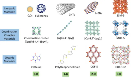
The approach of defining the dimensionality has changed in due course by both theoreticians and experimentalists and has been proved to show unusual physical properties in the fields of electronics5, spinotronics6, optonics7, photonics89, etc. In better understanding as in Figure 1.1 for
example, a 0-D can be thought as a single atom or a rather discrete group of caged molecules like fullerenes10 or non-caged cluster of atoms like QDs2,4,11or nanoparticles; similarly, CNTs12 or
1-D polymers1314 can be classified as examples of the 1-D materials. On the other hand, graphene15,16
being the first 2-D material has intrigued scientists for their unusual properties.
10 1.2 Classification of 2-D Layered Materials
Since the confinement of the bulk properties towards lower dimensionality has progressed much of its course, two-dimensional (2D) materials gained significant attention. After the discovery of graphene, interesting physical properties once predicted was seen to be existing, for example, Quantum Hall Effect (QHE)18,19, which intrigued scientists to research more about the 2-D
materials. In fact, in the field of material science and nanoscience, the anisotropy20 sheer induces
the variation in properties; in addition, the thickness (in nm scale) of such material improves the effect further. 2-D layered materials can be classified depending on its composition, synthetic procedure, application to be used for and etc. I would like to classify these layered materials by their composition in order to understand their electronics (dependent on different elements) and their applications (dependent on their energy distributions). Hence, 2-D materials can be categorized as follows: 1) single elemental 2-D layered material (example graphene comprising carbon), 2) inorganic 2-D layered material (example metal oxides, metal dichalcogenides, etc), 3) self-assembled 2-D layered material (metallic nanosheets), and 4) organic 2-D framework.
1.2.1 Single Elemental 2-D Layered Material
The first, of its kind, graphene, which is 2-D network of sp2 hybridized carbon in hexagonal lattice
retaining the extended -conjugation by aromaticity and discovered in 2004 by Novoselov and Geim15, was found to be the wonder material. With zero band gap21,22, it has a very high carrier
mobility5 following the relativistic Dirac equation23 for electron transport and the observation of
half integer Quantum Hall Effect (QHE)18 made the vintage theories come to life and its charge
carriers are massless Dirac fermions23 proved to be the beginning of new era of 2-D networks.
Unfortunately, of not having the bandgap in pristine graphene, sheet makes it harder for electronics as compared to silicon electronics. Although, band gap can be created and tuned by doping24,
stacking of small molecules25, covalent bonding26,27 or even increasing the thickness of layers21
which makes it usable in photonics8and optoelectronics9. General approach for this kind of single
elemental 2-D layered material is by top-down approach, yet nowadays bottom-up approach can be used like wet chemical synthesis28,29 for graphene and graphdiyne30. Graphene’s cousins like
11
of wonder materials, due to their band structure tuning compared to that of graphene, although few of them are yet to be synthesized. Thus, the research for a better 2-D material is essential for electronics.
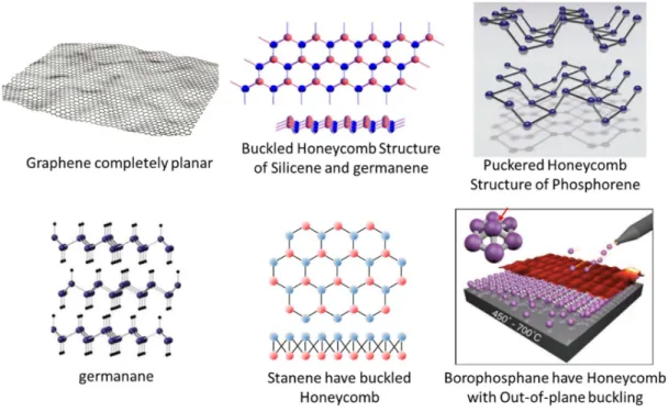
The other analogues of graphene have been the increasing research in the field of 2-D layered materials. Silicon imprints the sister graphene analogue called as silicene34–36. With buckled
honeycomb lattice and Dirac band structure37,38, it is possible to influence the band gap, band
structure and nano-electronics by external fields and interface interaction39. It has been predicted
that the Quantum Spin Hall effect40–43, chiral superconductivity44, giant magnetoresistance45 can
be seen in monolayer silicene. Similar to the silicene, germanium analogue named as germanene46
has also been reported. Multilayer hydrogen terminated germanane47 (GeH), analogues to
graphane structure, can be synthesized both by topochemical deintercalation of CaGe2 and
mechanical exfoliation47.
Figure 1.2.1 Structural differences among single elemental 2-D layered material15,46-48,53,54.
Taking steps with silicon and germanium, phosphorus has emerged with its class of 2-D layered materials called as phosphorene or phosphane48,49. The puckered honeycomb structure of
12
monolayer acts as semiconductor and a direct band gap of ~2eV was observed with layered dependent high charge carrier mobility48 ranging to ~1000 cm2 V-1s-1 for 10nm thick layers.
Transistor performance was seen in 7.5-nm thick layers with high order of drain current modulation in the order of 105 50. As for the other applications optoelectronics51, anode material
for sodium ion batteries52 and layered dependent photo assisted oxidation20 and quantum
confinement effects20 were also established for this class of 2-D material. Besides phosphorene,
crystalline 2-D boron sheets named as borophene53 were very recently synthesized where it forms
honeycombs of boron atoms with each hexagon capped with another boron atom forming an outer-plane buckling unlike boron nitride (BN)s as in Figure 1.2.1. Along with it was also seen that unlike other allotropes, borophene is found to be metallic53.
Moving forward from nonmetals like carbon, boron, phosphorus and metalloid like silicon and germanium, metals forming such network might be interesting as band structure is concerned. Recently, tin forming such networks called as stanene54 has been made successfully by epitaxial
growth. The prediction of room temperature QHE with enhanced thermoelectricity55 and
topological superconductivity56 increases the scope of research for the search of such kind 2-D
layered materials. It is interesting to note that group 14 elements are the point of all interest because of their interesting valence shell configurations.
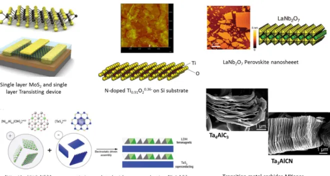
1.2.2 Inorganic 2-D Layered Materials
The top-down approach is substantially important for graphene, its analogue materials and for other kinds of robust inorganic layered materials as the search of the quantum properties is concerned. Boron nitrides57,58, transition metal dichalcogenides (TMDCs), transition metal oxides
and hydroxides, perovskite oxide141 and transition metal nitriles, carbides or carbonitrides
(MXenes) are the class of 2-D materials as in Figure 1.2.2 which are found to be having better properties than graphene due to the presence of direct bandgap for device fabrications.
Monolayers of transition metal dichalcogenides, with direct gap located at K-point, are thin semiconducting layered materials of type MX2 (M= Bi, Mo, W; X=S, Se, Te)59–64 can be
synthesized from exfoliation of bulk crystal (having indirect bandgap), chemical vapour deposition (CVD)60 and molecular beam epitaxy65. These are important as for transistors66 and
13
optoelectronics67 are concerned. The TMDCs having no inversion center, allowing new degrees of
freedom of charge carriers such as k-valley index61; hence, as far valleytronics68 is concerned, this
creates an interesting field of research in Physics. Further, strong spin-orbit splitting in monolayer leads to the building of spintronics devices.
Figure 1.2.2 Different examples of inorganic 2-D layered materials66,70,76,141,142.
On the other hand, transition metal oxides have been of much importance due to the catalysis69,
photocatalysis70, electronics, photovoltaics70, dielectrics and bio medical applications70, although
much of the metal oxides used are based on the titanium and manganese as the metal counter parts. Layered double hydroxides (LDH) of type [M2+1−x Al3+x(OH)2]x+ (M: Mg, Co, Ni, Zn)71,72 (0.2 ≤
x ≤ 0.33) have redox active magnetic properties70,142, while choice of metal (M) type would induce
properties like photoluminescence in case of type [RE3+(OH)2.5 xH2O]0.5+ (RE: Nd, Sm, Eu, Gd,
Tb, Dy, Ho, Er)73–75. Hydrophilic transition metal carbides (MXenes), like titanium carbides76–78,
14 1.2.3 Self Assembled 2-D layered material
This class of materials can be considered similar to previous category as in section 1.2.1, containing one single entity or group of entities, yet differs in the fact that the repeating unit forms self-assembled nano-architectures by mere cluster of metals or group of molecules through H-bonding79,80, van der Waals interaction or ionic interaction. Self-assembly81,82 of molecules like
pyrene83 or terrylene-based dye80, forming a bi-component supramolecular network with
melamine shows photo response80 intriguing possibilities in bottom-up fabrication of
optoelectronic devices. It is interesting to build supramolecular surface confined pores of different sizes84, conductive assemblies guided by DNA-strands by H-bonding interactions85,86 and the
host-guest chemistry and its molecular dynamics with the host-guest molecule, in particular porphyrins81,87
and its derivatives’ interacting with the substrate79 or guest molecule like heptamers of C6088
trapped within the cavities as in Figure 1.2.3.
Figure 1.2.3 Different examples of self-assembly81.
The free-standing ultrathin metallic nanosheets have been the research interest for number of applications in magnetism89–91, catalysis92, surface plasmonics resonance (SPR)92 and as
15
theranostic agents93. The metals that have been fabricated to such nano assemblies are Rh94, Ru95,
Pd92,96, Au97,98, Ag99, Fe100 and Cu101; even bimetallic systems like Pd@Ag102, Pd@Au93 or PtCu103
are important to integrate tuning of SPR and improve photothermal stability. Being metallic and free coordination site, especially noble metal nanosheets are mostly useful for the catalysis; PtCu for ethanol hydrogenation, Rh for hydroformylation of 1-octene and hydrogenation of phenol94.
The magnetic moments get enhanced from bulk crystal to single layers. The surfaces of single atom ferromagnetic layers’ example Fe100, have unsaturated coordination which directly leads to
the improved spin and orbital moments. Hence integrating such ultrathin metallic films with other 2D materials would result in better spin torque devices, spin polarizers or spin filters.
1.2.4 Organic 2-D framework
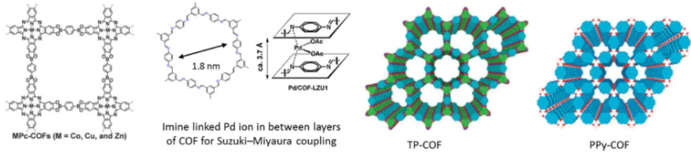
The organic 2-D frameworks or better known as the covalent organic framework (COFs) are the recent interest of robust class of covalent materials. In 2005, Yaghi and his co-workers first synthesized the porous organic crystalline 2D materials104. The joining of simple organic
molecules to a framework by using simple organic reaction, like boronate anhydride104 or ester
formation105, borosilicate formation106, nitrile cyclotrimerisation107, Schiff base formation108,
hydrazone formation109, led to new journey of COFs. Besides polymerization, porosity, structural
regularity and inducing functionality17,110 are the key factors for the development of such
framework. The application side of the COFs can be broadly of three types: a) photo electric applications, b) gas storage, and c) catalysis.
Figure 1.2.4 Different examples of COFs depending on their application17,110.
Introduction of different moieties like pyrene111,143, phthalocyanines112–114, porphyrins115–117
16
prepared by Jiang and co-workers is highly luminescent and harvests photons from ultraviolet to visible regions; in addition, it exhibits the p-type semiconductive111 characters due to the eclipsed
arrangement of triphenylene and pyrene units. COF features a remarkably large surface area and can be used for both gas adsorption and catalysis. Similar to zeolites, hybrids COFs can be heterogenous catalyst118, although only two examples are known, performing Suzuki-Miyaura108,
Sonogashira119, Heck or sequential one pot Heck-Sonogashira coupling reactions and
enantioselective high-yielding Michael reactions120. On the other hand, gas adsorption17,110 such
as hydrogen, methane, ammonia and carbon dioxide has been reported.
1.3 Importance of Bottom-Up Approach
Since 2004, exfoliation of the bulk crystals was the key way to produce different 2-D layered materials ranging from graphene to transition metal dichalcogenides. Due to usefulness of single layer for better performance and efficiency of fabricated device121, it is rather hard to produce large
films of such kind. Instead building up from simple units is rather considerable approach for better quality and controlled growth for such minute single layered devices. It has been proved that chemical vapor deposition CVD generates better quality material than mechanically exfoliated films. CVD is one of the versatile techniques applied for bottom-up approach of many 2-D layered materials122. For the tuning of physical properties like the electrochemical and charge mobility123,
n-doping in graphene can be one of the cheap solutions. There are reports of boron124, nitrogen125
phosphorus126 doping in graphene. All of these hetero atom dopings are carried out simultaneously
with CVD nanosheet preparation. Similar observation was also seen with transition metal dichalcogenides123. By using CVD technique, metal mixed chalcogenides122, MoS2/WS2
17 1.4 Coordination Nanosheet (CONASH)
In the light of considerable impact of 2-D layered material, there is a possibility that the framework can be built like as COFs, but instead of simple organic reaction to join two organic molecules, coordination chemistry can be used to coordinate metal and ligand moiety. This is advantageous to improvise 2-D COF to 2-D metal organic framework (MOF), as it gives more opportunities of catalytic site while considering the other applications unchanged. There is a room of full opportunities that can be considered for tuning the characteristics of the 2-D MOFs.
Figure 1.4.1 Different 2-D MOFs or coordination nanosheets (CONASHs)127-135, 138, 144.
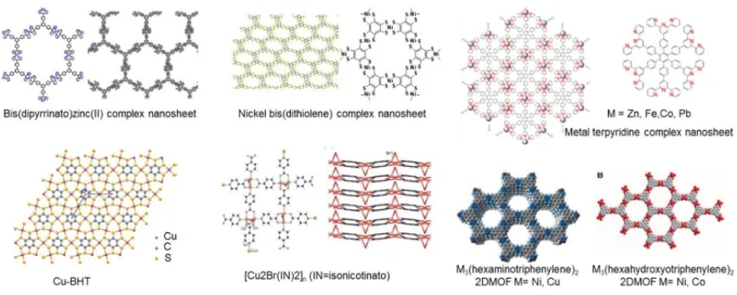
Comparing with other 2-D materials as described in previous sections, there is not much combinations except few metals and nonmetals but when we step into coordination nanosheets, we have whole range of coordination complexation including d-block and f-block metals with many combinations of p-block donor atoms. Moreover, this coordination happens easily at room temperature, hence higher elevated temperature as in case CVD may not be needed. Inducing functionality is easier through proper ligand design and metal choice. Dinca and co-workers have reported the nickel bis(hexaaminotriphennylene) complex nanosheets can electrochemically catalyze oxygen reduction reaction127 and has semiconducting nature128; while its copper analogue
sheet has ability to chemiresistive sensing129,130 properties as well. The point to be noted here is
the general procedure for synthesis of 2-D coordination polymer is via homogenous phase reaction containing both metal and ligand precursors. But Nishihara and coworkers showed interfacial
18
synthesis of 2-D polymers and explored interesting properties like change in oxidation states based on metal center of bis(terpyridine) Fe2+ or Co2+ complexes are functions of electrochromism131,
while replacing terpyridine moiety with bis(dipyrrinato)zinc(II) motif shows photoelectric conversion phenomenon132. In another case, change in the oxidation state based in the ligand center
of nickel bis(dithiolene) complex nanosheet is a function of conductivity133–135 up to 103 fold while
changing from Ni to Co metal, efficient hydrogen evolution136 from water has been reported by
Marinescu and coworkers.
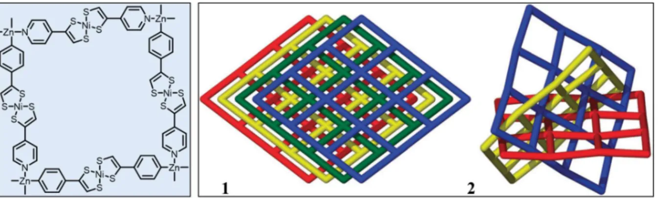
Interfacial reactions are more promising in order to make ordered structure. Polymers with large pores are often formed randomly in homogenous phase reactions resulting into an interpenetrated structure. For example, a layered planar polymeric structure might get interpenetrated with its own layers because of its large pore size forming 3-D structure and losses its planarity which might affect its physical properties thereby. Such an example is shown in Figure 1.4.2 b 137. But it has
been reported about the mono layer formation by interfacial synthesis which proves more efficient over the homogenous phase reaction.
Figure 1.4.2 One unit of the polymer (left); illustration of 1 and 2, each color represents a discrete 2D net stacked polymer and the interpenetrated structure of the same unit by forming coordination (right)137.
Band structure controls the general physical properties and in turn is a function of electron wave function of the distribution of atoms and molecules in the real space lattice which is directly guided by symmetry. Hence, symmetry is another important aspect of coordination complexation nanosheet. The symmetry of ligands and mode of coordination of metals play a vital role in defining the symmetry of the whole 2-D framework. For example, the symmetries of Cu-BHT138
19
complex nanosheet and nickel bis(dithiolene) complex nanosheet are completely different, in fact mode of coordination of Cu and Ni play a key role, although both the sheets diverge to a common ligand system. As a result of such difference in symmetry, the former shows a conductivity of 1580 S cm-1 while the later has a 160 S cm-1. Hence, simple symmetry of ligand design and mode of
20 1.5 Aim of Research
1.5.1 Background
Different ligand systems have been the back bone of coordination chemistry with the vibrant support of the different metals of the Periodic table. Diamines, dithiols as non-innocent complexes and its wide class of derivatives have been known for their conductive properties. Previously, Kambe et al. synthesized nickel bis(dithiolene) complex 2-D layered nanosheet135 having kagome
lattice by simple coordination polymerization of benzenehexathiol (BHT) ligand with Ni2+ ions.
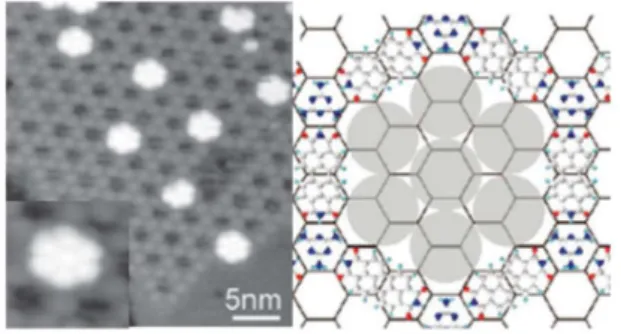
Later, Liu and coworkers theoretically predicted the single layer of aforementioned nanosheet to have topological insulator (TI)139 characteristics.
Figure 1.5.1 Prediction of TI characteristics of nickel bis(dithiolene) nanosheet139.
TI being the new state of matter has interested researcher due to their intrinsic property of conduction over the edges and not by bulk conductivity unlike normal conductors. The bulk band structure resembles as an insulator, yet the intrinsic phenomenon underlies that the symmetry protected surface states140 of such materials have a narrow gap and falls within the bulk gap. The
21
charge carriers are spin polarized i.e. the spin is locked at a right angle to their momentum (spin-momentum locking) hence there is no back scattering. It was also formulated that spin-orbit coupling (SOC) plays a vital role for the spin polarization as heavier elements increase the spin-orbit gap by splitting the topmost valence band so that SOC is strong enough to invert such insulating gap in case of TIs. Hence, building up such kind of 2-D coordinated layered material will be of much interest as for condensed matter physicists are concerned.
1.5.2 Problem Formulation
Taking a step further on replacing nickel by heavier metals of group 10 of nickel bis(dithiolene) the coordination complex nanosheet, it will be possible to increase SOC of the framework as the SOC increases down the group. Hence in my Ph.D. research, I focus at investigating on the synthetic strategies, electronic states and conductive behavior of heavier group 10 (Pd and Pt) metalladithiolene nanosheets due to the fact that heavier atoms have higher SOC. Additionally, it should be noted that their synthesis is highly challenging because the method to synthesize nickelladithiolene nanosheet by the reaction of Ni(II) ions and BHT cannot be simply applied because Pd(II) and Pt(II) system as they are easy to be reduced by thiols to their corresponding metallic state.
22 1.6 References:
1. Lovingood, D. D., Achey, R., Paravastu, A. K. & Strouse, G. F. Size- and site-dependent reconstruction in CdSe QDs Evidenced by 77Se {1H} CP-MAS NMR spectroscopy. J. Am.
Chem. Soc. 132, 3344–3354 (2010).
2. Lim, S. J., Zahid, M. U., Le, P., Ma, L., Entenberg, D., Harney, A. S., Condeelis, J. & Smith, A. M. Brightness-equalized quantum dots. Nat. Commun. 6, 1–10 (2015).
3. Gong, X., Yang, Z., Walters, G., Comin, R., Ning, Z, Beauregard, E., Adinolfi, V., Voznyy, O. & Sargent, E. H. Highly efficient quantum dot near-infrared light-emitting diodes. Nat. Photon. 10, 253–258 (2016).
4. Konstantatos, G., Badioli, M., Gaudreau, L., Osmond, J., Bernechea, M., Arquer, F. P. G., Gatti, F. & Koppens, F. H. L. Hybrid graphene–quantum dot phototransistors with ultrahigh gain. Nat. Nanotech. 7, 363–368 (2012).
5. Lin, Y., Dimitrakopoulos, C., Jenkins, K. A., Farmer, D. B., Chiu, H.-Y., Grill, A. & Avouris, Ph. 100-GHz Transistors from wafer scale epitaxial graphene. Science 327 , 662 (2010).
6. Kan, E., Li, M., Hu, S., Xiao, C., Xiang, H. & Deng, K. Two-dimensional hexagonal transition-metal oxide for spintronics. J. Phys. Chem . Lett. 4, 1120-1125 (2013).
7. Mueller, T., Xia, F. & Avouris, P. Graphene photodetectors for high-speed optical communications. Nat. Photon. 4, 297–301 (2010).
8. Bao, Q. & Loh, K. P. Graphene photonics, plasmonics, and broadband optoelectronic devices. ACS Nano 6, 3677–3694 (2012).
9. Bonaccorso, F., Sun, Z., Hasan, T. & Ferrari, A. C. Graphene photonics and optoelectronics. Nat. Photon. 4, 611–622 (2010).
10. Kroto, H. W. The stability of the fulerenes Cn, with n = 24,28,32,36,50,60 and 70. Nature
329, 529–531 (1987).
11. Courtney, C. M., Goodman, S. M., Mcdaniel, J. A. & Madinger, N. E. Photoexcited quantum dots for killing multidrug-resistant bacteria. Nat. Mater. 15, 529-535 (2016). 12. Sanchez-Valencia, J. R., Dienel1, T., Gro, O., Shorubalko, I., Mueller, A., Jansen, M.,
Amsharov, K., Ruffieux, P. & Fasel, R. Controlled synthesis of single-chirality carbon nanotubes. Nature 512, 61–64 (2014).
13. Fromm, K. M. Coordination polymer networks with s-block metal ions. Coord. Chem. Rev. 252, 856–885 (2008).
14. Welte, L., Calzolari, A., Di Felice, R., Zamora, F. & Gómez-Herrero, J. Highly conductive self-assembled nanoribbons of coordination polymers. Nat. Nanotech. 5, 110–115 (2010). 15. Novoselov, K. S., Geim, A. K., Morozov, S. V., Jiang, D., Zhang, Y., Dubonos, S. V.,
Grigorieva, I. V. & Firsov, A. A. Electric field effect in atomically thin carbon films. Science 306, 666–669 (2004).
23
16. Novoselov, K. S. & Geim, A. K. The rise of graphene. Nat. Mater. 6, 183–191 (2007). 17. Ding, S.-Y. & Wang, W. Covalent organic frameworks (COFs): from design to applications.
Chem. Soc. Rev. 42, 548–568 (2013).
18. Hsieh, D., Qian, D., Wray, L., Xia, Y., Hor, Y. S., Cava, R. J. & Hasan, M. Z. A topological Dirac insulator in a quantum spin Hall phase. Nature 452, 970–974 (2008).
19. Zhang, Y., Tan, Y., Stormer, H. L. & Kim, P. Experimental observation of the quantum Hall effect and Berry’s phase in graphene. Nature 438, 201–204 (2005).
20. Favron, A., Gaufrès, E., Fossard, F., Heureux, Anne-Laurence P.-L., Tang N. Y.-W., Lévesque, P. L., Loiseau, A., Leonelli, R., Francoeur, S. & Martel, R. Photooxidation and quantum confinement effects in exfoliated black phosphorus. Nat. Mater. 14, 826-833 (2015).
21. Zhang, Y., Tang, T.-Ta, Girit, C., Hao, Z., Martin, M. C., Zettl, A., Crommie, M. F., Shen, Y. R. & Wang, F. Direct observation of a widely tunable bandgap in bilayer graphene. Nature 459, 820–823 (2009).
22. Meric, I., Han, M. Y., Young, A. F., Ozyilmaz, B., Kim, P. & Shepard, K. L. Current saturation in zero-bandgap, top-gated graphene field-effect transistors. Nat. Nanotech. 3, 654–659 (2008).
23. Novoselov, K. S., Geim, A. K., Morozov, S. V., Jiang, D., Katsnelson, M. I., Grigorieva, I. V., Dubonos, S. V. & Firsov, A. A. Two-dimensional gas of massless Dirac fermions in graphene. Nature 438, 197–200 (2005).
24. Peimyoo, N., Li, J., Shang, J., Shen, X., Qiu, C., Xie, L., Huang, W. & Yu, T. Photocontrolled molecular structural transition and doping in graphene. ACS Nano 6, 8878– 8886 (2012).
25. Koehler, F. M., Jacobsen, A., Ensslin, K., Stampfer, C. & Stark, W. J. Selective chemical modification of graphene surfaces : distinction between single- and bilayer graphene. Small 6, 1125–1130 (2010).
26. Functionalized, G., Jeon, E. K., Kang, D., Kim, G., Kim,B.-S., Kang, D. J. & Shin, H. S. Reversibly light-modulated Dirac point of graphene functionalized with spiropyran. ACS Nano 6, 9207–9213 (2012).
27. Balog, R., Jørgensen, B., Nilsson, L., Andersen, M., Rienks, E., Bianchi, M., Fanetti, M., Lægsgaard, E., Baraldi, A., Lizzit, S., Sljivancanin, Z., Besenbacher, F., Hammer, B., Pedersen, T.G., Hofmann, P. & Hornekær, L. Bandgap opening in graphene induced by patterned hydrogen adsorption. Nat. Mater. 9, 315–319 (2010).
28. Cai, J., Ruffieux, P., Jaafar, R., Bieri1, M., Braun, T., Blankenburg, S., Muoth, M., Seitsonen, A. P., Saleh, M., Feng, X., Mṻllen, K. & Fasel, R. Atomically precise bottom-up fabrication of graphene nanoribbons. Nature 466, 470–3 (2010).
29. Tour, J. M. Top-down versus bottom-up fabrication of graphene-based electronics. Chem. Mater. 26, 163–171 (2014).
24
30. Haley, M. M. Synthesis and properties of annulenic subunits of graphyne and graphdiyne nanoarchitectures. Pure Appl. Chem. 80, 519–532 (2008).
31. Peng, Q., Dearden, A. K., Crean, J., Han, L., Liu, S., Wen, X. & De, S. New materials graphyne, graphdiyne, graphone and graphane : review of properties , synthesis , and application in nanotechnology. Nanotechnol. Sci. Appl. 7, 1–29 (2014).
32. Feng, L. & Zhang, W. X. The structure and magnetism of graphone. AIP Adv. 2, 042138 1-6 (2012).
33. Elias, D. C., Nair, R. R., Mohiuddin, T. M. G., Morozov, S. V., Blake, P., Halsall, M. P., Ferrari, A. C., Boukhvalov, D. W., Katsnelson, M. I., Geim, A. K. & Novoselov, K. S. Control of graphen's properties by reversible hydrogenation: evidence for graphane. Science 323, 610-613 (2009).
34. Resta, A., Leoni, T., Barth, C., Ranguis, A., Becker, C., Bruhn, T., Vogt, P. & Lay, G. L. Atomic structures of silicene layers grown on Ag(111): scanning tunneling microscopy and noncontact atomic force microscopy observations. Sci. Rep. 3, 2399 (2013).
35. Jose, D. & Datta, A. Structures and electronic properties of silicene: unlike graphene. Acc. Chem. Res. 47(2), 593-602 (2014).
36. Feng, J., Wagner, S. R. & Zhang, P. Interfacial coupling and electronic structure of two-dimensional silicon grown on the Ag ( 111 ) surface at high temperature. Nat. Publ. Gr. 1– 9 (2015).
37. Cahangirov, S., Topsakal, M., Aktu, E. & Ciraci, S. Two- and one-dimensional honeycomb structures of silicon and germanium. Phys. Rev. Lett. 102, 236804, 1–4 (2009).
38. Ni, Z., Liu, Q, Tang, K., Zheng, Z., Zhou, J., Qin, R., Gao, Z. Yu, D. & Lu, J. Tunable bandgap in silicene and germanene. Nano Lett. 12, 113–118 (2012).
39. Tao, L., Cinquanta, E., Chiappe, D., Grazianetti, C., Fanciulli, M., Dubey, M., Molle, A. & Akinwande, D. Silicene field-effect transistors operating at room temperature. Nat. Nanotech. 10, 227–231 (2015).
40. Liu, C., Feng, W. & Yao, Y. Quantum spin Hall effect in silicene and two-dimensional germanium. Phys. Rev. Lett. 107, 076802, 1–4 (2011).
41. An, X., Zhang Y., Liu, J. & Li, S. Quantum spin Hall effect induced by electric field in silicene. Appl. Phys. Lett. 102, 043113 1–5 (2013).
42. Tahir, M. & Schwingenschlo, U. Valley polarized quantum Hall effect and topological insulator phase transitions in silicene. Sci. Rep. 3, 1075, 1-5 (2013).
43. Ezawa, M. Quantum Hall Effects in Silicene. J. Phys. Soc. Japan 81, 064705 1–6 (2012). 44. Liu, F., Liu, C., Wu, K. Yang, F. & Yao, Y. d + id' Chiral superconductivity in bilayer
silicene. Phys. Rev. Lett. 111, 066804 1–5 (2013).
45. Xu, C., Luo, G., Liu, Q., Zheng, J., Zhang, Z., Nagase, S., Gao, Z. & Lu, J. Giant magnetoresistance in silicene nanoribbons. Nanoscale 4, 3111–3117 (2012).
25
46. Dávila, M. E., Xian, L., Cahangirov, S., Rubio, A. & Lay, G. Le. Germanene : a novel two-dimensional germanium allotrope akin to graphene and silicene. New J. Phys. 16, 095002 1-10, (2014).
47. Bianco, E., Butler, S., Jiang, S., Restrepo, O. D., Windl, W. & Goldberger, J. E. Stability and exfoliation of germanane : a germanium graphane analogue. ACS Nano 7, 4414–4421 (2013).
48. Li, L., Yu, Y., Ye, G. J., Ge, Q., Ou, X., Feng, D., Chen, X. H. & Zhang, Y. Black phosphorus field-effect transistors. Nat. Nanotechnol. 9, 372–377 (2014).
49. Brent, J. R., Savjani, N., Lewis, E. A., Haigh, S. J., Lewis, D. J. & O'Brien, P. Production of few-layer phosphorene by liquid exfoliation of black phosphorus. Chem. Commun. 50, 13338–13341 (2014).
50. Tayari, V., Hemsworth, N., Fakih, I., Favron, A., Gaufres, E., Gervais, G., Martel, R. & Szkopek T. Two-dimensional magnetotransport in a black phosphorus naked quantum well. Nat. Commun. 6, 7702 1–7 (2015).
51. Jia, Y., Xia, F. & Wang, H. Rediscovering black phosphorus as an anisotropic layered material for optoelectronics and electronics. Nat. Commun. 5, 1–6 (2014).
52. Sun, J., Lee, H. W., Pasta, M., Yuan, H., Zheng, G., Sun, Y., Li, Y. & Cui, Y. A phosphorene–graphene hybrid material as a high-capacity anode for sodium-ion batteries. Nat. Nanotech. 10, 980–985 (2015).
53. Mannix, A. J., Zhou, X. F., Kiraly, B., Wood, J. D., Alducin, D., Myers, B. D., Liu, X. & Fisher, B. L., Santiago, U., Guest, J. R., Yacaman, M. J., Ponce, A., Oganov, A. R., Hersam, M. C. & Guisinger, N. P. Synthesis of borophenes: anisotropic, two-dimensional boron poblymorphs. Science 350 , 1513-1516 (2013).
54. Zhu, F., Chen, W. J., Xu, Y., Gao, C. L., Guan, D. D., Liu, C. H., Qian, D., Zhang, S. C. & Jia, J. F. Epitaxial growth of two-dimensional stanene. Nat. Mater. 14, 1020- 1026 (2015). 55. Xu, Y., Gan, Z. & Zhang, S. C. Enhanced thermoelectric performance and anomalous
seebeck effects in topological insulators. Phys. Rev. Lett. 112, 226801 1–5 (2014).
56. Wang, J., Xu, Y. & Zhang, S. Two-dimensional time-reversal-invariant topological superconductivity in a doped quantum spin-Hall insulator. Phys. Rev. B 90, 054503, 1–5 (2014).
57. Tran, T. T., Bray, K., Ford, M. J., Toth, M. & Aharonovich, I. Quantum emission from hexagonal boron nitride monolayers. Nat. Nanotech. 11, 37-41 (2016).
58. Woessner, A., Lundeberg, M. B., Gao, Y., Principi, A., González, P. A., Carrega, M., Watanabe, K., Taniguchi, T., Vignale, G., Polini, M., Hone, J., Hillenbrand, R. & Koppens, F. H. L. Highly confined low-loss plasmons in graphene–boron nitride heterostructures. Nat. Mater. 14, 421–425 (2014).
59. Xu, X., Yao, W., Xiao, D. & Heinz, T. F. Spin and pseudospins in layered transition metal dichalcogenides. Nat. Phys. 10, 343-350 (2014).
26
60. Schmidt, H., Wang, S., Chu, L. Toh, M., Kumar, R., Zhao, W., Neto, A. H. C., Martin, J., Adam, S., Ȫzyilmaz, B. & Eda, G. Transport properties of monolayer MoS2 grown by
chemical vapor deposition. Nano Lett. 14, 1909-1913 (2014).
61. Zeng, H., Dai, J., Yao, W., Xiao, D. & Cui, X. Valley polarization in MoS2 monolayers by
optical pumping. Nat. Nanotech. 7, 490-493 (2012).
62. Ross, J. S., Klement, P., Jones, A. M., Ghimire, N. J., Yan, J., Mandrus, D. G., Taniguchi, T., Watanabe, K., Kitamura, K., Yao, W., Cobden, D. H. &Xu, X. Electrically tunable excitonic light-emitting diodes based on monolayer WSe2 p–n junctions. Nat. Nanotech. 9,
268–272 (2014).
63. Sun, L., Lin, J., Peng, J., Weng, J., Huang, Y. & Luo, Z. Preparation of few-layer bismuth selenide by liquid-phase-exfoliation and its optical absorption properties. Sci. Rep. 4, 4794 (2014).
64. Huang, C., Wu, S., Sanchez, A. M., Peters, J. J. P., Beanland, R., Ross, J. S., Rivera, P., Yao, W., Cobden, D. H. & Xu, X. Lateral heterojunctions within monolayer MoSe2 – WSe2
semiconductors. Nat. Mater. 13, 1096-1101 (2014).
65. Roy, A., Movva, H. C. P., Satpati, B., Kim, K., Dey, R., Rai, A., Pramanik, T., Guchhait, S., Tutuc, E. & Bannerjee, S. K. Structural and electrical properties of MoTe2 and MoSe2
grown by molecular beam epitaxy. ACS Appl. Mater. Interfaces 8, 7396-7402 (2016). 66. Radisavljevic, B., Radenovic, A., Brivio, J., Giacometti, V. & Kis, A. Single-layer MoS2
transistors. Nat. Nanotech. 6, 147-150 (2011).
67. Wang, Q. H., Kalantar-zadeh, K., Kis, A., Coleman, J. N. & Strano, M. S. Electronics and optoelectronics of two-dimensional transition metal dichalcogenides. Nat. Nanotech. 7, 699–712 (2012).
68. Mak, K. F., He, K., Shan, J. & Heinz, T. F. Control of valley polarization in monolayer MoS2 by optical helicity. Nature Nanotechnology 7, 494–498 (2012).
69. Feng, L., Fan, M., Wu, Y., Liu, Y. & Li, G. Metallic Co9S8 nanosheets grown on carbon
cloth as efficient binder-free electrocatalysts for the hydrogen evolution reaction in neutral media. J. Mater. Chem. A Mater. Energy Sustain. 4, 6860–6867 (2016).
70. Wang, L. & Sasaki, T. Titanium oxide nanosheets : graphene analogues with versatile functionalities. Chem. Rev. 114, 9455-9486 (2014).
71. Ma, R., Takada, K., Fukuda, K., Iyi, N., Bando, Y. & Sasaki, T. Topochemical synthesis of monometallic (Co2+-Co3+) layered double hydroxide and its exfoliation into positively
charged Co(OH)2 nanosheets. Angew. Chemie. Int. Ed. 47, 86–89 (2008).
72. Ma, B. R. & Sasaki, T. Nanosheets of oxides and hydroxides : ultimate 2D charge-bearing functional crystallites. Adv. Mater. 22, 5082–5104 (2010).
73. Lee, K.-H., Lee, B.-I., You, J.-H. & Byeon, S.-H. Transparent Gd2O3 : Eu phosphor layer
derived from exfoliated layered gadolinium hydroxide nanosheets. Chem. Commun. 46, 1461–1463 (2010).
27
74. Yoon, Y. S., Lee, B. I., Lee, K. S., Im, G. H., Byeon, S. H., Lee, J. H. & Lee, I. S. Surface modification of exfoliated layered gadolinium hydroxide for the development of multimodal contrast agents for MRI and fluorescence imaging. Adv. Funct. Mater. 19, 3375–3380 (2009).
75. Lee, B. I., Lee, K. S., Lee, J. H., Lee, I. S. & Byeon, S. H. Synthesis of colloidal aqueous suspensions of a layered gadolinium hydroxide: a potential MRI contrast agent. Dalton Trans. 14, 2490–2495 (2009).
76. Naguib, M., Mashtalir, O., Carle, J., Presser, V., Lu, J., Hultman, L., Gogotsi, Y. & Barsoum, M. W. Two-dimensional transition metal carbides. ACS Nano 6, 1322–1331 (2012).
77. Ghidiu, M., Lukatskaya, M. R., Zhao, M., Gogotsi, Y. & Barsoum, M. W. Conductive two-dimensional titanium carbide ‘clay’ with high volumetric capacitance. Nature 516, 78-81 (2014).
78. Halim, J., Lukatskaya, M. R., Cook, K. M., Lu, J., Smith, C. R., Naslund, L. A., May, S. J., Hultman, L., Ggotsi, Y., Eklund, P. & Barsoum, M W. Transparent conductive two-dimensional titanium carbide epitaxial thin films. Chem. Mater. 26, 2374-2381 (2014). 79. Gatti, R., MacLeod, J. M., Duffin, J. A. L., Moiseev, A. G., Perepichka, D. F. & Rosei, F.
Substrate, molecular structure, and solvent effects in 2D self- assembly via hydrogen and halogen bonding. J. Phys. Chem. C 118, 25505-25516 (2014).
80. Wieghold, S., Li, J., Simon, P., Krause, M., Avlasevich, Y., Li, C., Garrido, J. A., Heiz, U., Samori, P., Mullen, K., Esch, F., Barth, J. V. & Palma, C. A. Photoresponse of supramolecular self-assembled networks on graphene–diamond interfaces. Nat. Commun. 7, 10700 1–8 (2016).
81. Kudernac, T., Lei, S., Elemans, J. A. A. W. & Feyter, S. De. Two-dimensional supramolecular self-assembly : nanoporous networks on surfaces. Chem. Soc. Rev. 38, 402– 421 (2009).
82. Lit, J. V. D., Marsman, J. L., Koster, R. S., Jacobse,P. H., Hartog, S. A. D., Vanmaekelbergh, D., Gebbink, J. M. K., Filion, L. & Swart, I. Modeling the self-assembly of organic molecules in 2D molecular layers with different structures. J. Phys. Chem. C 120, 318-323 (2016).
83. Tuan, S., Pham, A. & Stöhr, M. Self-assembly of pyrene derivatives on Au(111): substituent effects on intermolecular interactions. Chem. Commun. 50, 14089–14092 (2014).
84. Schull, G., Douillard, L., Debuisschert, C. F. & Charra, F. Single-molecule dynamics in a self-assembled 2D molecular sieve. Nano Lett. 6, 1360–1363 (2006).
85. Yan, H., Park, S. H., Finkelstein, G., Reif, J. H. & Labean, T. H. DNA-templated self-assembly of protein arrays and highly conductive nanowires. Science 301, 1882-1884 (2003).
86. He, Y., Chen, Y., Liu, h., Ribbe, A. E. & Mao, C. Self-assembly of hexagonal DNA two-dimensional ( 2D ) arays. J. Am. Chem. Soc. 127, 12202–12203 (2005).
28
87. Wintjes, N., Bonifazi, D., Cheng, F., Kiebele, A., Stohr, M., Jung, T., Spillmann, H. & Diederich, F. A supramolecular multiposition rotary device. Angew. Chemie. Int. Ed. 46, 4089–4092 (2007).
88. Stöhr, M., Wahl, M., Spillmann, H., Gade, L. H. & Jung, T. A. Lateral manipulation for the positioning of molecular guests within the confinements of a highly stable self-assembled organic surface network. Small 3, 1336–1340 (2007).
89. Bruno, P. Tight-binding approach to the orbital magnetic moment and magnetocrystalline aisotropy of transition-metal monolayers. Phys. Rev. B 39, 865–868 (1989).
90. Qian, D., Jin, X. F., Barthel, J., Klaua, M. & Kirschner, J. Spin-density wave in ultrathin Fe films on Cu(100). Phys. Rev. Lett. 87, 227204 1-4 (2001).
91. Hjortstam, O., Trygg, J., Wills, J., Johansson, B. & Eriksson, O. Calculated spin and orbital moments in the surfaces of the 3d metals Fe, Co, and Ni and their overlayers on Cu(001). Phys. Rev. B 53, 9204–9213 (1996).
92. Huang, X.,Tang, S., Mu, X., Dai, Y., Chen, G., Zhou, Z., Ruan, F., Yang, Z. & Zheng, N. Freestanding palladium nanosheets with plasmonic and catalytic properties. Nat. Nanotech. 6, 28–32 (2011).
93. Chen, M., Tang, S., Guo, Z., Wang, X., Mo, S., Huang, X., Liu, G. & Zheng, N. Core-shell Pd@Au nanoplates as theranostic agents for in-vivo photoacoustic imaging, CT imaging, and photothermal therapy. Adv. Mater. 26, 8210–8216 (2014).
94. Duan, H., Yan, N., Yu, R., Chang, C. R., Zhou, G., Hu, H. S., Rong, H., Niu, Z., Mao, J., Asakura, H., Tanaka, T., Dyson, P. J., Li, J. & Li, Y. Ultrathin rhodium nanosheets. Nat. Commun. 5, 3093 1-8 (2014).
95. Yin, A. X., Liu, W. C., Ke, J., Zhu, W., Gu, J., Zhang, Y. W. & Yan, C. H. Ru nanocrystals with shape-dependent surface-enhanced raman spectra and catalytic properties: Controlled synthesis and DFT calculations. J. Am. Chem. Soc. 134, 20479–20489 (2012).
96. Yin, X., Liu, X., Pan, Y., Walsh, K. A. & Yang, H. Hanoi tower-like multilayered ultrathin palladium nanosheets. Nano Lett. 14, 7188-7194 (2014).
97. Huang, X., Li, S., Huang, Y., Wu, S., Zhou, X., Li, S., Gan, C. L., Boey, F., Mirkin, C. A. & Zhang, H. Synthesis of hexagonal close-packed gold nanostructures. Nat. Commun. 2, 292 1-6 (2011).
98. Niu, J., Wang, D., Qin, H., Xiong, X., Tan, P., Li, Y., Lu, X., Wu, J., Zhang, T., Ni, W. & Jin, J. Novel polymer-free iridescent lamellar hydrogel for two-dimensional confined growth of ultrathin gold membranes. Nat. Commun. 5, 3313 1-7 (2014).
99. Zhang, Q., Hu, Y., Guo, S., Goebl, J. & Yin, Y. Seeded growth of uniform Ag nanoplates with high aspect ratio and widely tunable surface plasmon bands. Nano Lett. 10, 5037–5042 (2010).
100. Zhao, J., Deng, Q., Bachmatiuk, A., Sandeep, G., Popov, A., Ecckert, J. & Rummeli, M. H. Free-standing single-atom-thick iron membranes suspended in graphene pores. Science 343
29 , 1228-1232 (2014).
101. Wu, Z., Li, Y., Liu, J., Lu, Z., Zhang, H. & Yang, B. Colloidal self-assembly of catalytic copper nanoclusters into ultrathin ribbons. Angew. Chemie. Int. Ed. 53, 12196–12200 (2014).
102. Huang, X., Tang, S., Liu, B., Ren, B. & Zheng, N. Enhancing the photothermal stability of plasmonic metal nanoplates by a core-shell architecture. Adv. Mater. 23, 3420–3425 (2011). 103. Saleem, F., Zhang, Z., Xu, B., Xu, X., He, P. & Wang, X. Ultrathin Pt − Cu nanosheets and
nanocones. J. Am. Chem. Soc. 135, 18304-18307 (2013).
104. Ockwig, N. W., Cote, A. P., Keeffe, M. O., Matzger, A. J. & Yaghi, O. M. Porous , crystalline , covalent organic frameworks. Science 310, 1166–1171 (2005).
105. Spitler, E. L. & Dichtel, W. R. Lewis acid-catalysed formation of two-dimensional phthalocyanine covalent organic frameworks. Nat. Chem. 2, 672–677 (2010).
106. Hunt, J. R., Doonan, C. J., LeVangie, J. D., Côté, A. P. & Yaghi, O. M. Reticular synthesis of covalent organic borosilicate frameworks. J. Am. Chem. Soc. 130, 11872–11873 (2008). 107. Kuhn, P., Antonietti, M. & Thomas, A. Porous, covalent triazine-based frameworks
prepared by ionothermal synthesis. Angew. Chemie. Int. Ed. 47, 3450–3453 (2008).
108. Ding, S.-Y., Gao, J., Wang, Q., Zhang, Y., Song, W. G., Su, C. Y. & Wang, W. Construction of covalent organic framework for catalysis: Pd/COF-LZU1 in Suzuki-Miyaura coupling reaction. J. Am. Chem. Soc. 133, 19816–19822 (2011).
109. Uribe-Romo, F. J., Doonan, C. J., Furukawa, H., Oisaki, K. & Yaghi, O. M. Crystalline covalent organic frameworks with hydrazone linkages. J. Am. Chem. Soc. 133, 11478– 11481 (2011).
110. Feng, X., Ding, X. & Jiang, D. Covalent organic frameworks. Chem. Soc. Rev. 41, 6010– 22 (2012).
111. Wan, S., Guo, J., Kim, J., Ihee, H. & Jiang, D. A belt-shaped, blue luminescent, and semiconducting covalent organic framework. Angew. Chemie. Int. Ed. 47, 8826–8830 (2008).
112. Ding, X., Guo, J., Feng, X., Honsho, Y., Guo, J., Seki, S., Maitarad, P., Saeki, A., Nagase, S. & Jiang, D. Synthesis of metallophthalocyanine covalent organic frameworks that exhibit high carrier mobility and photoconductivity. Angew. Chemie. Int. Ed. 50, 1289–1293 (2011).
113. Spitler, E. L., Colson, J. W., Uribe-Romo, F. J., Woll, A. R., Giovino, M. R., Saldivar, A. & Dichtel, W. R. Lattice expansion of highly oriented 2D phthalocyanine covalent organic framework films. Angew. Chemie. Int. Ed. 51, 2623–2627 (2012).
114. Ding, X., chen, L., Honsho, Y., Feng, X., Saengsawang, O., Guo, J., Saeki, A., Seki, S., Irle, S., Nagase, S., Parasuk, V. & Jiang, D. An n-channel two-dimensional covalent organic framework. J. Am. Chem. Soc. 133, 14510–14513 (2011).
30
115. Feng, X., Liu, L., Honsho, Y., Saeki, A., Seki, S., Irle, S., Dong, Y, Nagai, A. & Jiang, D. High-rate charge-carrier transport in porphyrin covalent organic frameworks: Switching from hole to electron to ambipolar conduction. Angew. Chemie. Int. Ed. 51, 2618–2622 (2012).
116. Wan, S., Gandara, F., Asano, A., Furukawa, H., Saeki, A., Dey, S. K., Liao, L., Ambrogio, M. W., Botros, Y. Y., Duan, X., Seki, S., Stoddart, J, F. & Yaghi, O, M. Covalent organic frameworks with high charge carrier mobility. Chem. Mater. 23, 4094–4097 (2011). 117. Feng, X., Chen, L., Dong, Y. & Jiang, D. Porphyrin-based two-dimensional covalent
organic frameworks: synchronized synthetic control of macroscopic structures and pore parameters. Chem. Commun. 47, 1979–1981 (2011).
118. Dogru, M., Sonnauer, A., Zimdars, S., Doblinger, M., knochel, P. & Bein, T. Facile synthesis of a mesoporous benzothiadiazole-COF based on a transesterification process. CrystEngComm 15, 1500–1502 (2013).
119. Pachfule, P., Panda, M. K., Kandambeth, S., Shivaprasad, S. M., Diaz, D. D. & Banerjee, R. Multifunctional and robust covalent organic framework–nanoparticle hybrids. J. Mater. Chem. A 2, 7944–7952 (2014).
120. Xu, H. & Gao, J. Stable , crystalline , porous , covalent organic frameworks as a platform for chiral organocatalysts. Nat. Chem. 7, 1–50 (2015).
121. Zhang, Y., Chang, T. R., Zhou, B., Cui, Y. T., Yan, H., Liu, Z., Schmitt, F., Lee, J., Moore, R., Chen, Y., Lin, H., Jeng, H. T., Mo, S. K., Hussain, Z., Bansil, A. & Shen, Z. X. Direct observation of the transition from indirect to direct bandgap in atomically thin epitaxial MoSe2. Nat. Nanotech. 9, 111–115 (2014).
122. Klee, V., Preciado, E., Barroso, D., Nguyen, A. E., Lee, C., Erickson, K. J., Triplett, M., Davis, B., Lu, I. H., Bobek, S., Mckinley, J., Martinez, J. P., Mann, J., Talin, A. A., Bartels, L. & Leonard, F. Superlinear composition-dependent photocurrent in CVD-grown monolayer MoS2(1−x)Se2x Alloy Devices. Nano Lett. 15, 2612-2619 (2015).
123. Yang, L., Majumdar, K., Liu, H., Du, Y., Wu, H., Hatzistergos, M., Hung, P. Y., Tieckelmann, R., Tsai, W., Hobbs, C. &Ye, P. D. Chloride molecular doping technique on 2D materials : WS2 and MoS2. Nano Lett. 14, 6275-6280 (2014).
124. Wu, T., Shen, H., Sun, L., Cheng, B., Liu, B. & Shen, J. Nitrogen and boron doped monolayer graphene by chemical vapor deposition using polystyrene , urea and boric acid. New J. Chem. 36, 1385–1391 (2012).
125. Bekyarova, E., Itkis, M. E., Ramesh, P., Berger, C., Sprinkle, M., Heer, W. A. D. & Haddon, R. C. Chemical modification of epitaxial graphene : spontaneous grafting of aryl groups. J. Am. Chem. Soc. 131, 1336–1337 (2009).
126. Li, R., Wei, Z., Gou, X. & Xu, W. Phosphorus-doped graphene nanosheets as efficient metal-free oxygen reduction electrocatalysts. RSC Advances 3, 9978–9984 (2013).
127. Miner, E. M., Fukushima, T., Sheberla, D., Sun, L., Surendranath, Y. & Dinca, M. Electrochemical oxygen reduction catalysed by Ni3(hexaiminotriphenylene)2. Nat.
31 Commun. 7, 10942 1-7 (2016).
128. Sheberla, D., Sun, L., Blood-Forsythe, M. A., Er, S., Wade, C. R., Brozek, C. K., Aspuru-Guzik, A. & Dinca, M. High electrical conductivity in Ni3
(2,3,6,7,10,11-hexaiminotriphenylene)2, a semiconducting metal-organic graphene analogue. J. Am.
Chem. Soc. 136, 8859–8862 (2014).
129. Campbell, M. G., Liu, S. F., Swager, T. M. & Dinca, M. Chemiresistive sensor arrays from conductive 2D metal-organic frameworks. J. Am. Chem. Soc. 137, 13780–13783 (2015). 130. Campbell, M. G., Sheberla, D., Liu, S. F., Swager, T. M. & Dinca, M.
Cu3(hexaiminotriphenylene)2: An electrically conductive 2D metal-organic framework for
chemiresistive sensing. Angew. Chemie. Int. Ed. 54, 4349–4352 (2015).
131. Takada, K., Sakamoto, R., Yi, S. T., Katagiri, S., Kambe, T. & Nishihara, H. Electrochromic bis(terpyridine)metal complex nanosheets. J. Am. Chem. Soc. 137, 4681–4689 (2015). 132. Sakamoto, R., Hoshiko, K., Liu, Q., Yagi, T., Nagayama, T., Kusaka, S., Tsuchiya, M.,
Kitagawa, Y., Wong, W. Y. & Nishihara, H. A photofunctional bottom-up bis(dipyrrinato)zinc(II) complex nanosheet. Nat. Commun. 6, 6713 1-9 (2015).
133. Kambe, T., Sakamoto, R., Kusamoto, T., Pal, T., Fukui, N., Hoshiko, K., Shimojima, T., Wang, Z., Hirahara, T., Ishizaka, K., Hasegawa, S., Liu, F. & Nishihara, H. Redox control and high conductivity of nickel bis(dithiolene) complex -nanosheet: A potential organic two-dimensional topological insulator. J. Am. Chem. Soc. 136, 14357–14360 (2014). 134. Hoshiko, K., Kambe, T., Sakamoto, R., Takada, K. & Nishihara, H. Fabrication of dense
and multilayered films of a nickel bis(dithiolene) nanosheet by means of the Langmuir-Schäfer method. Chem.Lett. 43, 252–253 (2014).
135. Kambe, T., Sakamoto, R., Hoshiko, K., Takada, K., Miyachi, M., Ryu, J. H., Sasaki, S., Kim, J., Nakazato, K., Takata, M. & Nishihara, H. -Conjugated nickel bis(dithiolene) complex nanosheet. J. Am. Chem. Soc. 135, 2462–2465 (2013).
136. Clough, A. J., Yoo, J. W., Mecklenburg, M. H. & Marinescu, S. C. Two-dimensional metal-organic surfaces for efficient hydrogen evolution from water. J. Am. Chem. Soc. 137, 118– 121 (2015).
137. Faust, T. B., Usov, P. M., D’Alessandro, D. M. & Kepert, C. J. Highly unusual interpenetration isomers of electroactive nickel bis(dithiolene) coordination frameworks. Chem. Commun. 50, 12772–4 (2014).
138. Huang, X., Sheng, P., Tu, Z., Zhang, F., Wang, J., Geng, H., Zou, Y., Di, C. A., Yi, Y., Sun, Y., Xu, W. & Zhu, D. A two-dimensional π-d conjugated coordination polymer with extremely high electrical conductivity and ambipolar transport behaviour. Nat. Commun. 6, 7408 1-8 (2015).
139. Wang, Z., Su, N. & Liu, F. T. Prediction of 2D organic topological insulator. Nano Lett. 13, 2842-2845 (2013).
32 3067 (2010).
141. Li, B. W., Osada, M., Ozawa, T. C., Ebina, Y., Akatsuka, K., Ma, R., Funakubo, H., and Sasaki, T. Engineered interfaces of artificial perovskite oxide superlattices via nanosheet deposition process. ACS Nano 4, 6673–6680 (2010).
142. Abellán, G., Gastaldo, C. M., Ribera, A., and Coronado, E. Hybrid materials based on magnetic layered double hydroxides: a molecular perspective. Acc. Chem. Res. 48, 1601−1611 (2015).
143. Wan, S., Guo, J., Kim, J., Ihee, H., and Jiang, D. A photoconductive covalent organic framework: self-condensed arene cubes composed of eclipsed 2D polypyrene sheets for photocurrent generation. Angew. Chem. 121, 5547-5550 (2009).
144. Amo-Ochoa, P., Welte, L., Prieto, R.G., Miguel, P. J. S., Gómez-García, C. J., Mateo-Martí, E., Delgado, S., Gómez-Herrerob, J., and Zamora, F. Single layers of a multifunctional laminar Cu(I,II) coordination polymer. Chem. Commun. 46, 3262–3264, (2010).
33
Chapter 2
-Conjugated Palladium Bis(dithiolene)
(PdDT) Coordination Nanosheets
34 2.1 Introduction
Research in 2-D coordination nanosheet (CONASH), or rather organic nanosheet, is now intensifying due to its versatility in tuning its properties over the whole range of periodic table by different combination of metals and strategic design of ligands forming isostructural inorganic lattices in ambient temperatures but also with specific optical-electronic properties. Previously, coordination polymerization of benenehexathiol (BHT) ligand with Ni2+ ions resulted in infinite
2-D layered multinucleated sheet1,2. Because of the increase in spin-orbit coupling (SOC), I
attempt a step further by utilizing the noble metal palladium, (having higher SOC value than nickel), as a candidate for CONASH. Noble metals are known for their positive reduction potentials and remain a challenge of using them with non-innocent hexathiol ligand system3, for
the fabrication of nanosheets. The use of interfacial reaction has proved to be useful for highly ordered, crystalline, layered material synthesis unlike the generation of amorphous material by monophasic reaction. In this work, I report the synthetic strategies and characterization of palladium bis(dithiolene) complex nanosheets (PdDT).
35
2.2 Liquid-Liquid Interfacial Synthesis of Palladium Bis(dithiolene) (PdDT) CONASH The pristine surface can be a mediating ground for reactions. We can exploit this kind of surfaces for the directional growth of the framework. In case of homogenous phase reaction, the framework will get intertwined as it lacks in directionality11. The framework being planar, the growth
directionality should be directed in x-y plane only. Out of solid, liquid, and gaseous medium reactions, liquid and gaseous phase reactions are more fast and controlled reactions compared to solids. The layering of two almost immiscible pair of liquids makes certain measured common phase. To understand this, for example, for water and CH2Cl2 system, which forms an azeotrope
mixture and solubility of CH2Cl2 in water being 17.5g/L at 25 ̊ C, when layered will always form
a very thin layer where both water and CH2Cl2 are miscible and is fixed depending on the volumes
of the pair of liquids. This can be a suitable site of reaction which will add the directionality to the growth of the framework4.
2.2.1 Synthesis of PdDT1
To synthesize PdDT, I employed the same approach similar to the case multilayer stacked nickel bis(dithiolene) CONASH or NiDT, which is a liquid-liquid interfacial reaction resulting to a high purity and larger domain of layered sheets. K2PdCl4 and NaBr in an aqueous phase and
benzenehexathiole (BHT) in an organic phase (dichloromethane) were layered in argon atmosphere. NaBr was added to supply counter cation for the anionic form of PdDT, [PdS4]- motif.
Figure 2.2.1 Fabrication of micro-PdDT. Both (a) and (b) illustrate liquid-liquid interfacial reaction and photography represent 1 and 2 (red arrow) at the interface, respectively.
36
After letting the two-phase solution standing overnight, a thin lustrous black film was formed at the interphase as shown in Figure 2.2.1a. Thickness of the PdDT film is around 2 - 3 µm and the film is referred to as PdDT1. The schematic equation is given in eq (i).
2.2.2 Results and Discussion of PdDT1
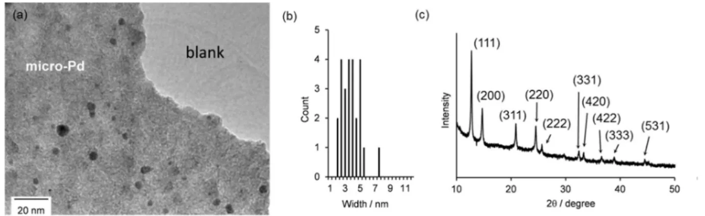
TEM measurement of PdDT1 displays a sheet material with some nm-scale grains (Figure 2.2.2 a,b). Powder XRD of PdDT1 shows several peaks characteristic of Pd(0) (Figure 2.2.2 c), implying that the observed grains are of metallic Pd(0)9. The TEM and XRD data reveal the
distribution of these grains of metallic Pd in the range of 3-5 nm diameter (Figure 2.2.2 b) which can be called as palladium nanoparticles PdNPs. The plausible reaction schemes are shown in Figure 2.3.1. This implies that the non-innocent BHT in dichloromethane has less positive potential than the Pd2+/Pd0 couple and acts as a reducing agent.
Figure 2.2.2 (a) TEM image showing PdDT1 sheet having black particles of Pd(0), (b) distribution of PdNPs as observed in (a). (c) Powder XRD data of (a). Observed peaks are corresponding to Pd(0) metal.
37
2.3 Liquid-Liquid Interfacial Synthesis of Nanoparticles Free PdDT
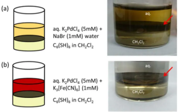
To prevent the formation of PdNPs, I introduced a layer of oxidizing agent, potassium ferricyanide (K3[Fe(CN)6]) in the aqueous layer to act as redox buffer which will prevent reduction of Pd2+ to
Pd(0) as given in eq(ii), before starting the liquid-liquid interfacial reaction as shown in Figure 2.3. The amount of K3[Fe(CN)6] strongly affects the film formation; addition of 1 mM K3[Fe(CN)6]
resulted in a formation of a black nanosheet with metallic luster, whereas 2 mM of K3[Fe(CN)6]
gave a pale blue material as shown in Figure 2.3. Further addition of K3[Fe(CN)6] formed
amorphous substance which does not have any sheet like morphology. The reaction condition A was found to be have sheet like morphology, so that further characterization was carried out with it and the sheet is called as PdDT2.
Figure 2.3 Photograph focusing on the water-dichloromethane interfaces with K3[Fe(CN)6] in the
aqueous layers. The concentrations of K3[Fe(CN)6] are 1 mM, 5 mM, 10 mM, and 20 mM in A,
38 2.4 TEM and Selected Area Diffraction of PdDT2
Transmission electron microscopy (TEM) displayed a sheet like morphology of PdDT2 in Figure 2.4 a. It is noteworthy that Pd(0) nanoparticles were not seen, which proves that K3[Fe(CN6)] acts
as an oxidizing agent and a redox buffer. In Figure 2.4 b, the edge has a stair like morphology which proves that it has a layered structure. Furthermore, selected area electron diffraction (SAED) showed a hexagonal diffraction pattern Figures 2.4 c, implying the skeleton of the framework has a hexagonal lattice with the in-plane cell length of 1.5 ± 0.1 nm. Plane indices shown in Figure 2.4c is fully consistent with the modelled kagome lattice structure and similar to NiDT nanosheets1.
Figure 2.4 (a) TEM image of PdDT2, (b) magnified view of (a), and (c) its selected area electron diffraction (SAED) pattern.
39 2.5 Infrared (IR) Spectroscopy of PdDT2
In the IR spectrum of PdDT2 (Figure 2.5), the strong S-H stretching vibration of BHT disappears completely. In addition, the broad C–S• stretching peak is observed at 1029 cm–1. Mononuclear
complex Pd(LBu)2 features three C–S• stretching peaks in the region of 1000-1100 cm–1 at the 0
oxidation state, whereas they change to a single peak at 1102 cm–1 in the –1 oxidation state1,5–7.
The observed broad peak at 1029 cm–1 assures that the 0 oxidation state is major in PdDT2.
40 2.6 X-ray Photoelectron Spectroscopy of PdDT2
XPS analysis of PdDT2 reveals the existence of each element (S, Pd, K) in Figure 2.6.1 and oxidation state of bis(dithiolato)palladium [PdS4]n (n=0, -1) units is reflected in the binding energy
of the S atom and is found by deconvolution of the S 2s envelope. Three deconvoluted bands emerge at 226.2, 227.7, and 232.6 eV for PdDT2 Figure 2.6.2 and Table 2.1 The first two are due to the -1 and 0 oxidation states of the [PdS4] motif, respectively, while the broad band at 230.5 and
232.6 eV are assignable to a ‘‘shake-up’’ peaks12,13, which are often observed in metal
bis(dithiolene) complexes1,8.
Figure 2.6.1 The S 2s (a), Pd 3d (b), K 2P (c) spectra of PdDT2.
Potassium ion is included as counter cation for both the anionic forms of PdDT, [bis(dithiolato)palladium(III)]-. Deconvolution of the S 2s peak indicates that the
[bis(dithiolato)palladium] unit is in the mixed valence state with 0 : –1 = 81 : 19 in PdDT2. We note that the valence is highly delocalized in PdDT, such that the oxidation number of the palladium bis(dithiolene) unit is uniform, adopting a value of –0.19. High ratio of the 0 oxidation state compared to micro-NiDT1 (0 : –1 = 74 : 26) is probably from the effect of the oxidant added
in the aqueous layer. Additionally, metal bis(dithiolene) complexes have their redox properties predominantly on the ligand center5. From these features, PdDT2 is suggested to possess the
41
mixed valence state of 0 and –1 similar to nickelladithiolene nanosheets (micro-NiDt and nano-NiDt)2- 1.
Figure 2.6.2 Deconvolutions of the S 2s peaks of PdDT2. The yellow and green Gauss curves are derived from the palladium bisdithiolene moieties with -1 and 0 oxidation states 1,3-6, respectively.
The gray one is assigned to the “shake-up” peak, which is often observed in bisdithiolene complexes12,13.
Table 2.1 Details of Deconvoluted S 2s XP Spectra
Band Position (eV) FWHM (eV) Area (%)
S2s band of PdDT2 1 226.2 2.5 15.0 2 227.7 3.3 64.9 3 232.6 3.7 20.1 220 225 230 235 240 Binding energies / eV In te ns ity / a. u.
42 2.7 Cyclic Voltammogram of PdDT1 and PdDT2
In fact, redox potentials in 0/–1 oxidation states of mononuclear complexes MII(LBu)2 (M = Ni,
Pd; LBu = 3,5-di-tert-butylbenzene-1,2-dithiolate ligands) are almost the same (–0.23 and –0.22 V vs ferrocenium/ferrocene)5. These data demonstrate that redox occurs on the ligand, and is nearly
independent of the central metal ion Ni or Pd. The cyclic voltammograms of PdDT1 and PdDT2 on HOPG are shown in Figure 2.7. A reversible redox wave was observed at 0.18 V and 0.27 V vs Ag+/Ag, which is ascribed to the 0/−1 redox couple of [PdS4] unit1,6. The wave derived from
the -1/-2 couple was not observed in the available potential window which is common for monomeric dithiolene complex5. At high scan rate, both reduction and oxidation waves disappear
implying that the electron transfer is very sluggish between reduced and oxidized palladium bis(dithiolene) motif of oxidation state -1 and 0, respectively.
Figure 2.7 Cyclic voltammograms1,6 PdDT1 (a) and PdDT2 (b) on ITO and HOPG,
43
2.8 Single Layer of Palladium Bis(dithiolene) CONASH
2.8.1 Synthesis by Gas-Liquid Interfacial Reaction of nano-PdDT
Figure 2.8.1 Synthesis of nano-PdDT.
The pristine surface being interesting site for reactions, thinner films can be anticipated via gas-liquid interfacial reactions. For nanoscience, control in the thickness is very important criteria. As explained previously, that the liquid-liquid interfacial reaction do not give control over the thickness in nm scale film formation. While spreading measured amount of ligand dissolved in ethyl acetate on surface of aqueous solution containing metal ion, the thickness of nanosheet in nm level can be controlled by the concentration of the ligand and the time of reaction.
BHT (30.4 µM) was gently spread to the surface (20.3 cm2) of an aqueous solution of K2PdCl4 (1
mM). The amount of BHT was restricted, so that it covered 30% - 70% of the aqueous surface area. The area covered with BHT was calculated using the space-filling model. After 15 minutes of standing time, nano-PdDT was deposited on a clean HOPG substrate by bringing the substrate close to the interface in the vertical direction (Langmuir-Schaefer (LS) method). The HOPG was then gently immersed in water, followed by ethanol and then ethyl acetate. It was then dried in vacuo for 48 hours. The samples for STM measurements were prepared by the same method as nano-PdDT but BHT covered 30% of the aqueous surface.
44 2.8.2 Atomic Force Microscopy (AFM) of nano-PdDT
A 2-D sheet like morphology can be seen under AFM. The structure can be clearly distinguished from the bare HOPG substrate in the AFM topographic image. However, small white spots ascribed to PdNPs are observed under AFM. I failed to find monolayers in the AFM image, instead, few layered nanosheet of 4 nm-10 nm were seen. This is probably due to severe - stacking between nanosheets.
Figure 2.8.2 AFM image of nano-PdDt. (a) AFM height image of topography image. (b) its cross-sectional analysis in (a).
2.8.3 Scanning Tunnelling Microscopy (STM) of nano-PdDT
Scanning probe microscopy (SPM) was exploited to determine the structure of atomically thin layered nanosheets. Thin sheets of nano-PdDT can be detected by STM as well as AFM measurements (Figure 2.8.2). Yet, by STM analysis I observed hexagonal patterns. The periodicity in STM image (Figure 2.8.3.1) of the hexagonal patterns (7.75 nm) was too large to be assigned directly to the in-plane lattice of nano-PdDT (1.5 ± 0.1 nm from (SAED) for PdDT2) nor for HOPG (0.246nm)1. Hence, the hexagonal periodicity observed is a moiré pattern conformed by
superimposition of two lattices: one is the in-plane of nano-PdDT and the other is derived from HOPG resulting the formation of a super lattice with a relative orientation angle of 1.78° (Figure 2.8.3.2). The same resulting periodicity can be simulated, which confirms that the moiré pattern is indeed due to the overlap between HOPG and PdDT CONASH.
45
Figure 2.8.3.1 (a) STM image of single layer nanosheet; Tip bias (Vtip) = -300 mV, (inset) Fast
Fourier Transform (FFT) of STM image, (b) magnified of area marked in (a).