INVITED PAPER
Special Section on Microwave and Millimeter-Wave TechnologyRecent Activities of Japanese Microwave Industry
Koji YAMANAKA†a), Yasunori SUZUKI††, Shoichi NARAHASHI††,Senior Members, Takaya WADA†††, Makoto KAWASHIMA†††,Nonmembers, Ken TAKEI††††,Member, Kazutaka TAKAGI†††††,Nonmember, Atsushi HONDA††††††, Zhengyi LI††††††,Members, Liang ZHOU††††††,Nonmember, Yoji OHASHI††††††,Member, Wataru HATTORI∗,andYusuke TAKAHASHI∗,Nonmembers
SUMMARY This invited paper is dedicated to introduce recent activi- ties of Japanese microwave industries. 7 topics are introduced from major microwave companies in Japan. All topics are from invited talks in 2014 Asia-Pacific microwave conference (APMC2014) held in Sendai, Novem- ber, 2014.
key words: microwave
1. Introduction
In APMC2014, many excellent papers were submitted from Japanese microwave industries. Among them, 7 papers are invited from Japanese major microwave related companies, namely Mitsubishi Electric Corp., NTT Docomo, Murata Manufacturing Co., Hitachi Ltd, Toshiba Corp., Fujitsu lim- ited and NEC Corp. They are all cutting-edge researches or most recent deployments of microwave technologies in Japan. In this paper, points of the 7 papers are introduced.
2. GaN Devices Employed in Infrastructure Systems (Yamanaka)
2.1 Solid State Weather Radar Systems
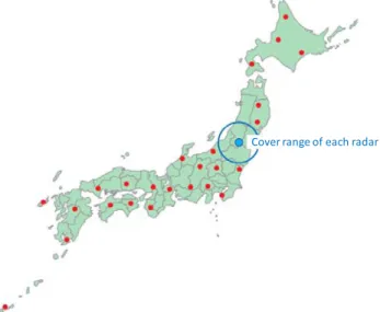
One of the most important applications of GaN devices in radar systems is the weather radar. Recently, extreme weathers like tornados and so-called guerrilla thunderstorms are observed quite often and sometimes cause loss of hu- man life. To save lives, weather radars are very impor- tant. There are 2 kinds of weather radar systems in Japan.
One is C-band radar systems to cover entire land of Japan Manuscript received April 3, 2015.
†The author is with Information Technology R&D Center, Mit- subishi Electric Corp, Kamakura-shi, 247–8501 Japan.
††The authors are with NTT Docomo, Yokosuka-shi, 239–8536 Japan.
†††The authors are with Murata Manufacturing Co., Ltd., Nagaokakyo-shi, 617–8555 Japan.
††††The author is with Hitachi Research Laboratory, Hitachi Ltd., Hitachi-shi, 319–1292 Japan.
†††††The author is with Komukai Complex, Toshiba Corporation, Kawasaki-shi, 212–8581 Japan.
††††††The authors are with Fujitsu Laboratories Ltd., Kawasaki-shi, 211–8588 Japan.
∗The authors are with NEC Corp., Kawasaki-shi, 273–8666 Japan.
a) E-mail: [email protected] DOI: 10.1587/transele.E98.C.621
Fig. 1 Allocation of C-band weather radar systems in Japan (reproduced from documents published by MLIT∗∗).
Fig. 2 GaN IM-FETs developed for weather radar systems (left: C-band 250W[1], right: X-band 120W[2]).
(Fig. 1). The other is X-band ones for the observation of local weather with higher resolution. Mitsubishi Electric has already developed both C-band and X-band GaN based radar systems. 250W C-band GaN amplifier[1]and 120W X-band GaN IM-FETs[2]are developed for this application (Fig. 2).
2.2 Satellite Communication Systems
C-band and Ku-band are popular frequency bands for satel- lite communication systems. GaAs devices have been used for small power terminals, e.g. V-SAT (very small aperture
∗∗MLIT: Ministry of of Land, Infrastructure, Transport and Tourism.
Copyright c2015 The Institute of Electronics, Information and Communication Engineers
Fig. 3 Ku-band 100W GaN IM-FET for satellite communication sys- tems[2].
terminals), while traveling wave tube amplifiers (TWTAs) have been employed for large power systems, e.g. satel- lite news gathering (SNG) systems and satellite loaded sys- tems. At C-band low efficiency of GaAs has been com- plaint of the users. However, 67% efficiency of GaN IM- FET[3] resolved the problem. In Ku-band, low power of GaAs was addressed with more than 100W output power of GaN (Fig. 3)[2]. Such high power also contributes to re- place TWTAs with GaN devices in SNG systems.
3. Base Station Digital Pre-Distortion Compensat- ing for Frequency-Dependent IMD Components (Suzuki and Narahashi)
Future base station power amplifiers (PAs) should offer lower power consumption, light weight, and miniaturiza- tion. Therefore, the output back-off should be reduced through the linearization techniques to help achieve the goals described above. However, it is known that the PA generates complicated inter-modulation distortion (IMD) components that are frequency dependent when reducing the output back-off. This section presents progress in the research of the digital pre-distorter proposed in[4]and[5]
(hereinafter referred to as proposed DPD) that compensates for frequency-dependent IMD components.
3.1 Proposed DPD
Figure 4 shows the basic configuration of the proposed DPD[4] which is based on a power-series DPD, and is equipped with a frequency characteristics compensator to suppress frequency-dependent IMD components. The pro- posed DPD sets the sample amplitude and the anti-phase at each frequency point, and the controller uses a coefficient calculation method[5] which directly calculates the coeffi- cients of the vector regulator and the frequency characteris- tics compensator based on the relationship between the co- efficients and the IMD components using the measurement results. Figure 5 shows the proposed dual-band DPD con- figuration which has two third-order distortion generation paths to compensate for the third-order IMD components in each band, and two third-order distortion generation paths to compensate for the cross-term IMD components. The con- troller of the dual-band DPD has the same configuration as
Fig. 5 Basic configuration of proposed dual-band DPD.
Fig. 6 Drain efficiency vs. ACLR.
that of the single band DPD.
3.2 Experimental Results
Figure 6 shows the experimental results of the drain effi- ciency of a PA with and without the proposed DPD. The PA has the saturation output power of 30 dBm in the 2 GHz band with class-AB biasing. The employed test signal is an orthogonal frequency division multiplexing signal with 64 sub-carriers at the center frequency of 2.14 GHz. It employs quadrature phase shift keying (QPSK) modulation and has the bandwidth of 3.84 MHz. The proposed DPD with and without the frequency characteristics compensator achieves the drain efficiency of 16% and 11%, respectively, when the adjacent channel leakage power ratio (ACLR) is−45 dBc.
The proposed DPD improves the drain efficiency because the frequency-dependent IMD components are suppressed.
Figure 7 shows the experimental results of dual-band simultaneous amplification with the proposed DPD when inputting the QPSK modulated test signals at the center frequencies of 2.6 GHz and 2.7 GHz, and the bandwidth of 3.84 MHz. The PA has the saturation output power of 50 W with class-A biasing. The vector regulators are set to the optimum values for 2.6 GHz and 2.7 GHz opera-
Fig. 7 ALCR performance at dual-band operation.
tions. The frequency characteristics compensators are not used in this experiment because the PA does not have the frequency-dependent IMD components. Figure 4 shows the worst ALCR performance at each frequency. The proposed dual-band DPD can simultaneously compensate for the IMD components at 2.6 GHz and 2.7 GHz bands.
3.3 Conclusion
This section presented progress in the research of the pro- posed DPD that compensates for frequency-dependent IMD components. There are still technical issues that need to be addressed such that the proposed DPD incurs a calculation cost for the frequency characteristic compensators.
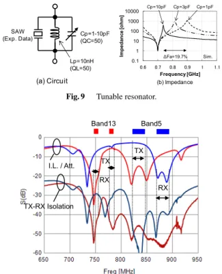
4. A New Tunable RF Front-End for Advanced 4G Handsets (Wada and Kawashima)
A new tunable RF front-end solution is proposed and its ef- fectiveness is shown experimentally. For the solution, novel devices such as a tunable duplexer, comprised of a wide band circulators and tunable SAW filters, and a tunable low RX noise PA have been developed for the whole LTE and UMTS low-band frequency range. The measured sup- pression values of RX band noise have reached to 50dB in Band5 and Band13. Those results indicate that the solution is strongly promising for a single chain tunable front-end of cellular terminals.
4.1 Circuit Configuration and Devices
In current cellular systems, the number of frequency bands which are specified in the 3rd Generation Partnership Project (3GPP) standard has been increasing[6]. In order to simplify the complex RF front-end circuit of the cellular handset, authors have proposed a new single chain tunable RF front-ends for three paths each (low band, medium band and high band), using wideband circulators, SAW-based tunable filters and tunable low RX noise PAs as shown in Fig. 8[7]. This paper presents the design and experimental results for the low-band circuit and devices.
For the SAW-based tunable filters, new spurious free wide band Love-wave resonators have been developed, and by using expansion inductors and variable capacitors, ade- quate tunable range of 31.5% has been obtained. Figure 9
Fig. 8 Proposed solution using circulators, tunable filters and tunable low RX noise PAs.
Fig. 9 Tunable resonator.
Fig. 10 Measured tunable duplexer module of Band5 and 13 tuned case.
shows typical characteristics of the tunable resonator. In or- der to realize the new miniaturized (1.8×1.6×0.5mm3) wide band circulator, a very weak magnetic field condition below the ferromagnetic resonance has been applied to a lumped element circulator. To reduce the RX band noise of the PA, the similar type of tunable SAW resonators have been em- bedded between the cascaded amplifiers as tunable band re- jection filters.
4.2 Evaluation Results and Conclusions
In combination with the developed tunable filters for TX and RX and wide band circulator, the tunable duplexer module was fabricated. The measurement results of the isolation from TX port to RX one and the attenuation from TX to ANT for Band 5 and 13 are shown in Fig. 10.
In both bands, more than 40dB isolation has been ob- tained.
Regarding the developed low RX nose PA, more than 10dB improvement is achieved compared with conventional
Wireless Systems (Takei)
A novel antenna, whose structure is automatically generated by computer using a brute-force algorithm, is introduced. At a glance, this antenna appears to consist of randomly allo- cated square patches, and it is difficult to guess its perfor- mance which exceeded that of a conventional antenna with the same gain and bandwidth.
5.1 Introduction
Computer assisted design is very useful for developing mi- crowave devices because their actual performances can be very accurately simulated by computer using Maxwell’s equation and electrical circuit theory. Therefore, the con- ceptional design of microwave devices can be performed by using a high performance computer and sophisticated cal- culation algorithms. This report introduces novel antennas that are designed by computer in the conceptional phase and explains the algorithms that are used for these conceptional designs.
5.2 Random-Pattern Antenna for Mobile Device
A random-pattern antenna (RPA) is a planar antenna whose two-dimensional structure consists of many small square patches. The antenna design requires a lot of repeats of randomly generated patches in the limited area where the antenna is enclosed and many calculations of the gain and bandwidth performances of all of them. Our strategy is simply to repeat such generation and calculation at a much higher speed than that of conventional technologies by using a newly developed method to calculate matrix equations.
5.2.1 Inverse Matrix Reverse Equation Method[8]
The voltage flow depends on the voltage occurring in the narrow gap between segments and is rigorously defined at the area of two absent adjacent segments within the frame- work of an MoM formulation. The voltage flow V and the induced current I are related to each other and can be derived by using the exiting source Ve and impedance matrix Z as
[Z]
I 0
≡
ZII ZIV
ZV I ZVV
I 0
= Ve
0
+ 0
V
(1) The induced currents determine every antenna characteris- tic, including the input impedance, gain, axial ratio, radia- tion efficiency, and far-field pattern. Equation (1) is derived from two matrix equation systems whose unknowns are the induced current and voltage flow as
Fig. 11 Built-in antenna for RFID reading module.
[ZII] I
= Ve
, Y≡Z−1 [YVV]V
=−[YV I]Ve
,I
=[YII]Ve
+[YIV]V (2-a,b)
Since Eqs. (2-a) and (2-b) are transformed into each other by using the inverse matrix and reciprocal quantity with physically reverse meaning, the electromagnetic char- acteristics of the antenna can be calculated only by the in- duced currents or voltage flows.
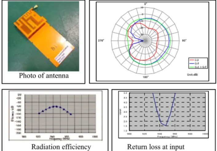
5.2.2 Built-In Antenna for RFID Reader Module[9]
A built-in antenna for RFID reading module that is inserted into Japanese commercial cell phones was designed and manufactured. The compact RFID reading module, whose size was 0.06×0.16×0.001λ, was achieved by using very thin random-pattern planar structure.
The voltage-flow design drastically reduces the number of unknowns to calculate EM performances.
Figure 11 shows the photo, radiation pattern, radiation efficiency and return loss at input of the antenna.
6. GaN HEMTs are Still Ongoing (Takagi)
6.1 AlGaN/GaN HEMTs with Field-Plate
Field-plates were necessary for reducing the current col- lapse, but they also decreased the gain by increasing the parasitic capacitance. Two kinds of AlGaN/GaN epitax- ial wafers were used in this study, called “Epi wafer A”
and “Epi wafer B”. “Epi wafer B” has considerably lower- density trap states than “Epi wafer A”. Three device struc- tures were then fabricated on both wafers. They were (a) without a source field plate, (b) with a source field plate Lsfp =0.5μm and (c) Lsfp =1.5μm. All devices had the same gate length (Lg) of 0.6μm and a total gate width of 540μm (270μm×2).
Figure 12 shows the drain efficiencies of the devices.
When the harmonics were shorted, each device showed al- most the same drain efficiency. But when the harmonics
Fig. 12 Dependency of the drain efficiency on the epitaxial wafer and the device structure. The devices were biased at Vds=40 V at a fundamental frequency of 3.0 GHz on a harmonic tuning active loadpull system.
Fig. 13 A device with two 35mm-gate-width dies which had a source field plate of 0.5μm produced output power reached 461W (56.64dBm) with a 15.44dB related gain and 59.4% of PAE at a drain voltage of 50V under the pulsed condition of 200μs pulse width and 10% duty cycles.
were optimized, each device showed a difference.
For devices fabricated on “Epi wafer A”, the drain effi- ciency increased with the longer source field plate. In con- trast, for devices fabricated on “Epi wafer B”, the drain effi- ciency decreased with the longer source field plate. And the drain efficiencies of “Epi wafer B” were higher than those of “Epi wafer A”. Both the device without a source field plate, and the device with a source field plate of 0.5μm on
“Epi wafer B” showed a drain efficiency of 84%, which was about 20% higher than that of “Epi wafer A”. To achieve high efficiency, the harmonics control needed a gain at the harmonics frequencies which were two or three times higher than the fundamental frequency.
Figure 13 shows the power characteristics of two 35mm-gate-width dies which had a source field plate of 0.5μm. The measured output power reached 461W with a 15.44dB related gain and 59.4% of PAE at a drain voltage of 50V.
6.2 AlGaN/GaN HEMTs without Field-Plate
At millimeter-wave frequencies, since it is more difficult to
Fig. 14 MMIC 16 cells for an output power stage (6.4mm), which was driven by 8 FET cells for the driver stage (3.2mm), achieved a saturated out- put power of 42.8dBm (19W) to 43.3dBm (21W) across 29GHz to 31GHz at VDD=28V under the pulsed condition of 100μs pulse width and 10%
duty cycles.
realize a high gain, special attention was paid to the for- mation of the epitaxial layer structure, the gate fabrication techniques and the layout pattern.
A 50μm gate-width 8-finger cell was designed for the millimeter-wave frequency. A Loadpull measurement was performed on the FET cell to determine the optimum load impedance using a passive-tuner system at 31GHz. The cell achieved a saturated output power of 31.2dBm (3.3W/mm), an associated gain of 7dB and PAE of 40%.
A 2-stage MMIC was designed with 16 cells for the output power stage (6.4mm) which was driven by 8 FET cells for the driver stage (3.2mm). The MMIC achieved a saturated output power of 19W to 21W across 29GHz to 31GHz as shown in Fig. 14.
7. Development of Wireless Communication Technolo- gies for Future Multi-Gigabit Data Transmission (Honda, Li, Zhou, and Ohashi)
Recently, several new applications such as 5th generation cellular communications or mobile backhaul systems are studied for realization of large communication capacity and cost reduction of base station. Meanwhile, low frequency bands such as VHF or UHF bands are already tightly used because of high date rate communication for multiple users.
To realize high data rate communications, it is mandatory to use more high frequency bands, where there are wide band- widths available for communications. However, the energy consumption would be enlarged if wide band transceivers are employed, so the studies of improvement of frequency efficiency are required to minimize the energy consumption and cost of transceivers. In this paper, we introduce commu- nication techniques to improve data rate at millimeter wave band using spatial multiplexing.
7.1 Millimeter-Wave Transmission Equipment
Table 1 summarize the transmission parameters. The sys- tem employs OFDM scheme for data transmission, the data
Besides, we introduce LOS-MIMO techniques for spatial multiplexing that are suitable for high frequency band com- munications such as millimeter wave communications.
For anN×NLOS-MIMO link with Uniform Linear Ar- ray (ULA), channel orthogonality can be obtained if the cor- relation between the different columns is equal to zero[11].
For a given rangeR0 and carrier wavelengthλ, the optimal antenna separationd for ULA MIMO systems is given by whenR0d,
d= λR0
N . (3)
Under the condition (3), the channel matrix becomes orthog- onal. Figure 16 shows eye-pattern of received signal of 2×2 LOS-MIMO system, the bit rate is 1Gbps for each antenna branch. We have confirmed the realization of spatial multi- plexing at LOS environment from the experiments.
Table 1 Summary of Transmission Parameters.
Fig. 15 RF measurement results of the test equipment. (a) Transmit spectrum. (b) Received signal after coherent detection (16 QAM).
Fig. 16 Eye patterns of 2×2 LOS-MIMO transmissions.
used, however, there are still many places where they can- not be applied. For examples; blind spots, crowded places with poor visibility, privacy-minded locations such as lava- tories, and so on. A presence sensor-sheet is a prospective candidate for monitoring such places instead of cameras.
The conventional presence sensor-sheets are mostly based on pressure sensors. These pressure sensors-sheets are nor- mally used for limited purposes such as researches, though they have developed for more than 10 years. The reasons are that they are too expensive to cover large area, and that they require special flooring materials which must conduct pressure.
We developed inexpensive presence sensor-sheets to detect objects and persons with no RFID tags attached[12], [13] by applying tag-antenna-based sensing (TABS)[14]
proposed by MIT Auto-ID Lab and near-field RFID tech- nology. MIT’s TABS provides presence sensing function to an ordinary passive ultra-high-frequency (UHF) RFID tag with the cost of only around 10 yen using the dependency of the tag antenna operation on its surrounding. This TABS adopted far-field radio wave propagation between a reader and tag antennas. Then, frequent tag reading errors occur due to non-line-of-sight conditions and multipath radio in- terference. These errors lead to false detection, which is fatal for practical usage.
To solve this problem, we employed wireless coupling between a near-field traveling-wave reader antenna and an antennas of passive UHF RFID tags as illustrated in Fig. 17.
Since the reader and tag antennas are closely arranged, noth- ing can easily enter between them and block the communi- cation through the coupling. In addition, this system is free from the multipath interference because the signal strength through the coupling is dominantly larger than those of in- terference waves. In this system, the presence of an ob- ject on a tag can be detected by the reduction of the signal strength. When nothing is on the tag, its antenna operates as a resonator and the reflected signal from the tag to the reader is strong. When something is on the tag, however, the res- onant operation of its antenna is inhibited, and the reflected
Fig. 17 Sensor unit configuration of our proposed sensor-sheet.
Fig. 18 Beverage bottle detection. (a) Setup of 120 beverage bottles on a shelf. (b) Detected results; Bottle mark shows presence of beverage bottle at corresponding position.
Fig. 19 Recognition of footprint. (a) Three persons standing on a proto- type sheet. (b) Footprint recognition results. Orange blobs indicate recon- structed region from tag signals. Open squares show blobs recognized as footprints.
signal strength decreases.
We applied the technology for detecting beverage- bottles and human footprints. Figure 18 (a) shows the demonstration of detection of 120 beverage bottles on a triple-stage shelf. Forty beverage bottles were arranged on a sensor-sheet on each stage. Each tag embedded in the sheet was placed beneath the corresponding bottle position. The detected results were displayed by bottle marks on a PC as shown in Fig. 18 (b). If TABS is applied to this case, it is difficult to install far-field antennas where the line-of-sight radio paths to all the tags can be ensured. This system is ap- plicable to real-time inventory and stock-out detection with no tag attached on each item unlike the conventional RFID systems, and it results in low-consumption of time, effort, and cost.
Figure 19 (a) shows a prototype sensor-sheet for foot- print recognition covered by a solid poly-carbonate plate.
After the signals from embedded tags were visualized to the orange-scaled blobs through intensity normalization and spatially interpolation, the blob was recognized as a foot- print by pattern recognition as framed in by an open square in Fig. 19 (b).
This sensor-sheet is superior to conventional pressure- sensor-sheets in the durability since a solid flooring mate- rial can be adopted. This is because that the surface ma-
terial needs to conduct not pressure, but electro-magnetic field sufficiently. Additionally, there is no need to attach the RFID tag on someone’s body. This provides monitor- ing people without identifying the individuals, that is, while protecting their privacy.
9. Conclusion
7 recent Japanese microwave industry activities presented in APMC2014 invited talks are introduced in this paper.
References
[1] H. Maehara, H. Uchida, N. Kosaka, E. Kuwata, K. Yamanaka, J.
Nishihara, K. Kawashima, and M. Nakayama, “Internally Matched GaN FET at C-band with 220W Output Power and 56% Power Added Efficiency,” 2012 Asia Pacific Microwave Conference Dig., pp.358–360, Dec. 2012.
[2] H. Noto et al, “X- and Ku-band Internally Matched GaN Amplifiers with more than 100W output power,” 2012 European Microwave Integrated Circuits Conference Dig., pp.695–698, Oct. 2012.
[3] S. Miwa, Y. Kamo, Y. Kittaka, T. Yamasaki, Y. Tsukahara, T.
Tanii, M. Kohno, S. Goto, and A. Shima, “A 67% PAE, 100 W GaN Power Amplifier with On-Chip Harmonic Tuning Circuits for C-band Space Applications,” 2011 IEEE MTT-S Int. Microwave Symp. Dig., WE3D-1, June 2011.
[4] S. Mizuta, Y. Suzuki, T. Hirota, and Y. Yamao, “Digital predis- tortion linearizer for compensating frequency-dependent IM distor- tion,” Proc. 34th European Micro. Conf., pp.1053–1056, 2004.
[5] J. Ohkawara, Y. Suzuki, and S. Narahashi, “Fast calculation scheme for frequency characteristic compensator of digital predistortion lin- earizer,” Proc. Vech. Tech. Conf. Spring, pp.1–5, 2009.
[6] 3GPP standardization http://www.3gpp.org/
[7] H. Obiya, T. Wada, H. Hayafuji, T. Ogami, M. Tani, M. Koshino, M.
Kawashima, and N. Nakajima, “A New Tunable RF Front-End Cir- cuit for Advanced 4G Handsets,” 2014 IEEE MTT-S Int. Microwave Symp. Digest, session WEP-54, June 2014.
[8] K. Takei and T. Ogawa, “Increment-Decrement Algorithm for Com- pact Circularly Polarized Antenna,” Proc. ICECom, Dubrovnic, pp.1–4, Oct. 2005.
[9] K. Takei, “Computational design of wireless interface for RFID reader module applied to mobile devices,” Proc. ECCSC 2010, Bel- grade, pp.216–219, Nov. 2010.
[10] T. Umaba, S. Kitazawa, A. Miura, H. Ohtsuki, M. Ueba, M. Azuma, A. Honda, S. Shimizu, “Demonstration experiment of millime- ter wave multi-gigabit wireless LAN system,” IEEE RFIT 2009, pp.28–31, Dec. 2009.
[11] L. Zhou and Y. Ohashi, “Design of non-uniform antenna arrays for robust millimeter-wave LOS MIMO communications,” IEEE PIMRC 2013, pp.1397–1401, Sept. 2013.
[12] W. Hattori, K. Ohashi, and H. Fukuda, “Tag-Antenna-Based Pres- ence Sensing Using Near-Field Traveling-Wave Reader Antenna,”
Proc. Internet of Things 2014, pp.103–107, 2014.
[13] W. Hattori, H. Fukuda, K. Takahashi1, R. Kawai, Y. Takahashi, and H. Miyano, “Near-Field RFID Sensor-Sheets to Detect Objects and Persons with No RFID Tags Attached,” Proc. APMC 2014, pp.486–488, 2014.
[14] R. Bhattacharyya, C. Floerkemeiner, and S. Sarma, “Low-cost, ubiq- uitous RFID-tag-antenna-based sensing,” Proc. IEEE, vol.98, no.9, pp.1593–1600, 2010.
and GaN high power amplifiers. He received the Best Paper Prize in GAAS2005 for the pa- per entitled “S and C band Over 100W GaN HEMT 1-chip High Power Amplifiers with Cell Division Configuration”.
Yasunori Suzuki received the B.E. and M.E.
degrees from Nagaoka University of Technol- ogy, Niigata, Japan, in 1993 and 1995, respec- tively, and the Ph.D. degree from Hokkaido Uni- versity, Sapporo, Japan, in 2011. In 1995, he joined NTT Mobile Communications Network (now NTT DOCOMO, INC.) where he was en- gaged in research on base station equipment for mobile communications. He is currently a Se- nior Research Engineer of Research Laborato- ries. He is a member of the IEEE.
Shoichi Narahashi received the B.E.
and M.E. degrees from Kumamoto University, Kumamoto, Japan, in 1986 and 1988, respec- tively, and the Ph.D. degree from Hokkaido Uni- versity, Sapporo, Japan, in 2008. In 1988, he joined Radio Communication Systems Labora- tories, Nippon Telegraph and Telephone (NTT) Corporation where he was engaged in research and development on base station equipment for digital mobile communications. Since 1992, he has been with NTT DOCOMO, INC. He is cur- rently an Executive Research Engineer, Group Leader of Research Labora- tories with the mission of investigating RF technologies for mobile commu- nications. Dr. Narahashi was the recipient of the 2011 IEICE Achievement Award and the 2012 IEICE Best Paper Award. He is a member of the IEEE, EuMA, IEEJ and the Society of Instrument and Control Engineers (SICE).
Takaya Wada was born in Japan in 1972.
He received the master’s degree in electrical and electronic engineering from Toyohashi Uni- versity of Technology, Aichi, Japan in 1996.
Currently, he is the senior manager of the Mi- crowave Technology Development Department at Murata Manufacturing Co., Ltd., involved in research and development efforts in Tunable fil- ter, Circulator and Front-end modules.
Ken Takei was born in Tokyo, Japan in 1960. He received the B.S. and M.S. de- grees in electric and electronic engineering from Tokyo Institute of Technology, Japan, in 1983 and 1985, respectively. In 1985 he joined Cen- tral Research Laboratory, Hiatchi Lid., where he had been engaged in the development of wire- less devices. In 2003 he joined Hitachi Cable Lyd. and had been engaged in the development of antennas for 3 years. He has been engaged in the development of highly secure wireless net- works from 2010 in Hitachi Research Laboratory.
Kazutaka Takagi received his master’s degree in engineering from Tokyo Metropoli- tan University. Since 1988, he has been with Toshiba Corporation, where he has been en- gaged in the development of compound semi- conductor electron devices. He has created many GaAs MESFET products, and is currently focusing on GaN based electron devices.
Atsushi Honda received the B.E. de- gree in electrical and electronic engineering in 2003 from Tokyo Institute of Technology, Japan.
Since 2003 he has been with Fujitsu Labora- tories Ltd., Kawasaki, Japan. His current re- search interests are millimeter-wave circuits and antenna technologies for wireless communica- tions.
Zhengyi Li was born in China. He re- ceived the B.E. degree in Information Engi- neering from Xi’an Jiaotong University, Xi’an, China, in 2004, and the Ph.D. degree in Elec- tronic Engineering from Tsinghua University, Beijing, China, in 2010. From 2010 to 2012, he was a Postdoctoral Researcher at the Research Center for Frontier Medical Engineering, Chiba University, Japan. Since April 2012, he has been a Researcher at Fujitsu Laboratories Ltd., Japan.
In October 2013, he visited Karlsruhe Institute of Technology (KIT), Karlsruhe, Germany. His research interests include millimeter wave commutation, small antennas for body-centric wireless communications, MIMO antennas, and reconfigurable antennas. Dr. Li is a Member of European Microwave Association (EuMA), and also a Member of the Institute of Electronics, Information and Communication Engineers (IEICE), Japan. He was the recipient of the 2010 Asia-Pacific Radio Sci- ence Conference (AP-RASC’10) Young Scientist Award, and the recipient of the 2013 IEEE Antennas and Propagation Society (IEEE AP-S) Japan Chapter Young Engineer Award.
Liang Zhou received the B.S. and M.S.
degrees in electrical engineering from Beijing Normal University, China, in 1983 and 1986 respectively, and the Ph.D. degree in intelli- gent science from Tokyo Institute of Technol- ogy, Japan, in 1997. From 1986 to 1993, he was with Sichuan University, Chengdu, China.
Since 1997, he has been with Fujitsu Laborato- ries Ltd., Kawasaki, Japan. His research experi- ence includes pattern recognition, speech signal processing, low power VLSI and DSP processor design. His current research interests include signal processing for wire- less communications, space time processing, MIMO-OFDM, LOS-MIMO, millimeter wave communications.
Yoji Ohashi received the B.S. in physics in 1984 and the M.S. in astronomy in 1986 from Nagoya University, Japan. Since 1986 he has been with Fujitsu Laboratories Ltd., Kawasaki, Japan. His research experience in- cludes millimeter-wave circuits and packages design. His current research interests include millimeter-wave radar and communication sys- tems.
Wataru Hattori received the B.E. and M.E.
degrees from Osaka University, Osaka, Japan, in 1992 and 1994, respectively, and Ph.D. degree from Tokyo University, Tokyo, Japan, in 2002.
He joined NEC Corporation in 1994, and cur- rently is a principal researcher of the Green Plat- form Research Labs., NEC Corp., Kawasaki, Japan. Since 2012, he has been engaged in the research and development on presence sensing systems using RFID. Dr. Hattori was the recipi- ent of the 1999 Spring Young Scientist Oral Pre- sentation Award presented by the Japan Society of Applied Physics (JSAP).
He is a member of the IEEE and JSAP.
Yusuke Takahashi received the B.E. de- gree from Tokyo Institute of Technology, Tokyo, Japan in 1995, and M.E. degree from Univer- sity of Sao Paulo, Sao Paulo, Brazil in 1997. He joined NEC Corporation in 1997, and currently is a senior researcher of the NEC Laboratories Singapore, NEC Asia Pacific, Singapore. Since 2013, he has been engaged in the research and development on presence sensing systems using image analysis and machine learning.
![Fig. 3 Ku-band 100W GaN IM-FET for satellite communication sys- sys-tems[2].](https://thumb-ap.123doks.com/thumbv2/123deta/5625256.1500139/2.892.472.801.108.693/fig-ku-band-gan-fet-satellite-communication-tems.webp)