• 検索結果がありません。

2017‑03‑10

N/A
N/A
Protected

Academic year: 2021

シェア "2017‑03‑10"

Copied!
297
0
0

読み込み中.... (全文を見る)

全文

(1)

Near‑Field Devices

Author Mark Daly

Degree Conferral Date

2017‑03‑10

Degree Doctor of Philosophy Degree Referral

Number

38005甲第1号 Copyright

Information

(C) 2017 The Author

URL http://doi.org/10.15102/1394.00000167

(2)

Graduate University Thesis submitted for the degree

Doctor of Philosophy

Light-Induced Interactions using Optical Near-Field Devices

by

Mark Daly

Supervisor: Prof. Síle Nic Chormaic

October, 2016

(3)

Declaration of Original and Sole Authorship

I, Mark Daly, declare that this thesis entitled Light-Induced Interactions using Optical Near-Field Devices and the data presented in it are original and my own work.

I conrm that:

• This work was done solely while a candidate for the research degree at the Okinawa Institute of Science and Technology Graduate University, Japan and the University College Cork, Ireland.

• No part of this work has previously been submitted for a degree at this or any other university.

• References to the work of others have been clearly attributed. Quotations from the work of others have been clearly indicated, and attributed to them.

• In cases where others have contributed to part of this work, such contribution has been clearly acknowledged and distinguished from my own work.

Date: October, 2016 Signature:

ii

(4)

Light-Induced Interactions using Optical Near-Field Devices

Optical near-elds are generated when light passes through components with wavelength, or subwavelength features. The near-elds generated at the surfaces of devices are often neglected, in part because the far-elds have more applications and are more readily accessible. Near-elds, as one might expect, occur very close to the surface of the material through which the light passes. However, near-elds present an interesting method of overcoming Rayleigh's diraction limit. For example, the evanescent eld at the surface of a prism or ultrathin bre rapidly decays, but can exist in sub-diraction limited areas.

Similarly, the eld generated by a subwavelength aperture or a plasmonic particle can have local eld distributions with minute dimensions, allowing one to conne light to areas otherwise unattainable, extremely close to the surface of the material in question.

By exploiting this aspect of optical near-elds we apply them to problems in atom and particle trapping.

Our main focus is on ultrathin optical bres. These bres dier from telecommunica- tions bre due to their lack of cladding material and their wavelength-scale dimensions.

These two factors combine to produce a signicant evanescent eld at their waist. This eld is readily accessible and can be used to trap particle or atoms through the optical forces which arise in such light-matter interactions. We can also use such devices to pas- sively collect light which is emitted into the available guided mode. Here, we demonstrate how an ultrathin bre can be used as a probe to determine the temperature of a cold atom cloud.

Ultrathin bres, while extremely useful, have some limiting factors related to the

strength and distribution of their evanescent elds. To improve upon the design, we also

investigated how one can nanostructure an optical bre using focussed ion beam milling

techniques or combine optical bres with gold dimer arrays to produce localised eld

enhancements. We used nanostructured bres to trap 100 and 200 nm dielectric spheres

within the structured region. Various numerical techniques were employed to characterise

(5)

both the nanostructured bre and the plasmonic-enhanced bre.

Aside from optical bres, we also briey discuss how an array of Fresnel microlenses

can be packaged with other atom chip designs to produce a device which could trap atoms

microns away from a gold surface. We discuss the theory and fabrication technique for

such a Fresnel microlens array atom chip.

(6)

Acknowledgement

After many years of PhD research there is a seemingly uncountable number of people of whom I need to acknowledge. But, I would like to start with perhaps the most important person during my research career so far, my supervisor, Prof. Síle Nic Chormaic. She has guided my research for so many years, both as part of the Quantum Optics Group in Ireland, and as part of the Light-Matter Interactions group in Japan. I am extremely thankful for all her help and support, and especially her patience, during my PhD years.

I hope that she will continue to guide many more students in the years to come.

During my time as a PhD student I had the pleasure to work with many people from all over the world. For many of these people it is dicult to pinpoint how exactly they helped me throughout my career, but I'll begin by thanking all of the group members I have worked with, past and present, for their support both academically and personally.

Thank you Aili, Ramgopal, Ravi, Mary, Ivan, Marios, Ciarán, Michael, Vu, Laura, Eugen, Krishnapriya, Thomas, Peter, Alex, Amy, Yuqiang, Vibhuti, Vandna, Yong, Kristoer, Aysen, Metin, Elaine, Alan, Bishwajeet, Sunny, Nitesh, Sho, Tridib, Jinjin, Wenfang, Xue, Fuchuan, Ratnesh, Ali (Seer), Sanele, Sahar, Cindy, Yuta, Lisa, Jan, Christiane, Vikraman, and Tushar. I'd like to especially thank Dr. Kieran Deasy, Dr. Viet Giang Truong, and Dr. Jonathan Ward for working closely with me throughout my PhD and providing me with invaluable advice and information. And I must also acknowledge Emi Nakamura for the incredible amount of work she has done for me throughout the years.

I must also acknowledge the technical support sta from OIST, UCC, and the Tyndall National Institute who have assisted me in both my technical training as well as producing

v

(7)

high quality devices when required. I would especially like to thank Dr. Laszlo Szikszai and Dr. Toshio Sasaki who were instrumental in my technical training at OIST. I must also thank the academic support sta at UCC and OIST. Margaret Bunce helped me many times at UCC, and the Student Support sta at OIST have always provided me with a friendly face to speak with despite bringing them an increasing number of problems to deal with. I'd also thank Dr. Kishan Dholakia for his support during my thesis proposal;

his advice following my exam was extremely benecial. I also thank Dr. Thomas Busch for being my mentor during my time at OIST, his wonderful sense of humour helped to improve my mood on many occasions.

I would also like to thank Dr. Jonathan Dorfan for his role as the president of OIST during its formative years. His phone call a week following the interview process allowed me to continue my work in physics to this day.

Aside from the technical support, I would also like to thank all of my friends, both from the past and the many new ones I have made during my PhD. It is safe to say that I would not have made it through my PhD without their support and company.

Finally I would like to thank my parents, Josephine and Mark, my sister Sarah-Jane,

and my wonderful girlfriend Emily for the years of support, fun, and love that they have

supplied me with, as well as my extended family who have always been supportive of my

studies.

(8)

Abbreviations

AOM Acousto-Optical Modulator DAQ Data Acquisition

EDS Energy Dispersive X-ray Spectroscopy FIB Focussed Ion Beam

EBID Electron Beam Induced Deposition STOF Slotted Tapered Optical Fibre FDTD Finite Dierence Time Domain FEM Finite Element Method

HE Hybrid Electric ITO Indium Tin Oxide MNF Micro/nanobre MOT Magneto-Optical Trap MST Maxwell Stress Tensor LP Linearly Polarised

LSPR Localised Surface Plasmon Resonance PD Photodiode

PSD Power Spectral Density SLM Spatial Light Modulator TE Transverse Electric TM Transverse Magnetic

OMA Orbital Angular Momentum

vii

(9)

R-S Rayleigh-Sommerfeld

SAS Saturated Absorption Spectroscopy SEM Scanning Electron Microscopy SIBA Self-Induced Back Action

SPCM Single Photon Counting Module SPP Surface Plasmon Polariton STOF Slotted Tapered Optical Fibre TOF Time-of-Flight

UHV Ultra High Vacuum

(10)

Nomenclature

c Speed of light ( 2.997 924 58 × 10 8 ms −1 )

~ Reduced Planck constant ( 1.054 572 66 × 10 −34 Js) k B Boltzmann constant ( 1.380 658 × 10 −23 JK −1 )

0 Permittivity of free space ( 8.85418782 × 10 −12 ) µ 0 Permeability of free-space ( 4π × 10 −7 Hm −1 ) n air/vacuum Refractive index of air (1)

n water Refractive index of water (1.33) n silica Refractive index of silica (1.45591)

λ Wavelength of light ω Frequency of light

~k Wave vector of light

β Propagation constant of light in a waveguide E ~ Electric eld

D ~ Electric displacement eld B ~ Magnetic eld

H ~ Magnetic intensity ( B/µ ~ 0 ) ρ Charge density

j Current density

J n , K n Bessel functions of the rst and second kind, respectively

σ ± Circularly polarised light with positive and negative handedness

85 Rb Rubidium isotope with 85 neutrons

ix

(11)

F Total atomic angular momentum J Total electronic angular momentum

I Nuclear angular momentum T D Doppler-limited temperature

γ Scattering rate

s 0 Saturation parameter I Intensity of light I s Saturation intensity µ 0 Magnetic moment of atom

C 3 C 3 parameter of the Lennard-Jones potential

(12)

included here.

(13)

Contents

Declaration of Original and Sole Authorship ii

Abstract iii

Acknowledgement v

Abbreviations vii

Nomenclature ix

Contents xii

List of Figures xvii

List of Tables xxi

1 Introduction 1

1.1 Applications . . . . 3

1.2 Optical Trapping Regimes . . . . 4

1.2.1 Rayleigh Regime . . . . 5

1.2.2 Mie Solutions and Discrete Dipole Approximation . . . . 7

1.2.3 Other Forces . . . . 9

1.3 Optical Tweezers with Free-Space Laser Beams . . . . 9

1.3.1 Optical Tweezers Basics . . . 10

xii

(14)

1.3.2 Dual Beam Optical Tweezers . . . 14

1.4 Trapping via Integrated Optics . . . 16

1.4.1 Channel Waveguides . . . 17

1.4.2 Optical Micro-Nanobres . . . 19

1.4.3 Slot Waveguides . . . 20

1.4.4 Photonic Crystal Cavities . . . 23

1.4.5 Microlenses . . . 26

1.5 Plasmonic Based Devices . . . 26

1.5.1 Surface Plasmon Polaritons and Localised Surface Plasmons . . . . 27

1.5.2 Scalability . . . 29

1.5.3 Self-Induced Back Action . . . 30

1.5.4 Super Resolution Optical Trapping . . . 32

1.5.5 Gratings . . . 34

1.5.6 Plasmonic Nanorods and Ultrathin Fibres . . . 35

1.5.7 Subwavelength Apertures . . . 37

1.6 Conclusion . . . 41

2 Fundamentals of Optical Fibres and Optical Trapping 43 2.1 Ultrathin Optical Fibres . . . 44

2.1.1 Maxwell's Equations and the Wave Equation . . . 46

2.1.2 Optical Fibre Modes in MNFs . . . 47

2.1.3 Fibre Pulling . . . 48

2.2 Optical Forces . . . 50

2.2.1 Maxwell Stress Tensor . . . 51

2.2.2 Dipole Approximation . . . 53

2.2.3 Mie Scattering . . . 54

2.2.4 Minkowski Force Density . . . 56

2.3 Atom Trapping . . . 58

(15)

2.3.1 Energy Levels in 85 Rb . . . 59

2.3.2 Cooling and Trapping . . . 60

2.4 Plasmonic Enhancement . . . 63

2.4.1 Quasi-static Approximation . . . 63

2.4.2 The Dipole Hybridization Model . . . 65

2.5 Conclusions . . . 66

3 Forced Oscillation Temperature Measurement Using an Ultrathin Fibre 68 3.1 Alternative Measurement Techniques . . . 70

3.1.1 Time-of-Flight . . . 70

3.1.2 Release and Recapture . . . 71

3.1.3 Forced Oscillation Method . . . 71

3.2 Sub-Doppler Temperature Measurements using an Ultrathin Fibre . . . 74

3.2.1 Ultrathin Optical Fibres in a Vacuum Chamber . . . 75

3.2.2 Experimental Setup . . . 76

3.2.3 Timing and Triggering . . . 80

3.2.4 Results . . . 82

3.3 Conclusions . . . 86

4 Slotted Tapered Optical Fibre for Atom Trapping 89 4.1 Guided Modes of the System . . . 91

4.1.1 Optical Mode Distributions . . . 91

4.1.2 Mode Denition . . . 95

4.2 Trap Design . . . 97

4.2.1 Surface Interaction Potential . . . 97

4.2.2 Optically Produced Potential and Atom Trapping . . . 99

4.2.3 Trapping Potential . . . 101

4.2.4 Atom Trap Viability . . . 109

4.3 Slot Endface Geometry . . . 110

(16)

4.4 Conclusion . . . 114

5 Particle Trapping using Ultrathin Optical Fibres 117 5.1 STOF Fabrication . . . 121

5.1.1 Tapering Process . . . 122

5.1.2 Coating Process . . . 122

5.1.3 Etching Process . . . 124

5.1.4 Alternative Approaches . . . 126

5.2 Transmission Characteristics of STOFs . . . 127

5.3 Experimental Setup . . . 128

5.3.1 Ultrathin Optical Fibres and Slotted Tapered Optical Fibres . . . . 128

5.3.2 Field Distribution . . . 128

5.3.3 Experimental Outline . . . 130

5.3.4 Polarisation Preparation . . . 133

5.4 Numerical Analysis . . . 134

5.5 Additional Considerations . . . 138

5.5.1 Multiple Particle Scattering . . . 138

5.5.2 Thermophoretic Forces . . . 140

5.6 Results and Trap Analysis . . . 142

5.7 Conclusion . . . 146

6 Plasmon Enhanced Ultrathin Fibres 148 6.1 Design and Fabrication . . . 149

6.1.1 Electron Beam Induced Deposition . . . 151

6.1.2 FEM Simulations . . . 152

6.2 Characterisation . . . 154

6.2.1 SEM Imaging . . . 154

6.2.2 Energy-Dispersive X-ray Spectroscopy and Oxygen Plasma Treatment156

6.2.3 Absorption Measurements . . . 158

(17)

6.3 Conclusions . . . 160

7 Fresnel Microlens Array for Atom Trapping 162 7.1 Fresnel Atom Microlens . . . 163

7.1.1 Wave Diraction Optics . . . 163

7.1.2 Atom Potential . . . 164

7.1.3 U- & Z-chips . . . 166

7.1.4 Fabrication . . . 169

7.2 Reection Spectra . . . 172

7.3 Conclusion . . . 173

Conclusion 177 8 Conclusion 177 8.1 Thesis Summary . . . 177

8.2 Impact and Future Work . . . 178

8.3 Final remarks . . . 180

A Solutions to the Scalar Helmholtz Equation Mie Scattering 182

B Relevant Code and Model Files 185

Bibliography 186

Published articles 213

(18)

List of Figures

1.1 Mie interference eects . . . . 8

1.2 Gaussian beam optical tweezers . . . 11

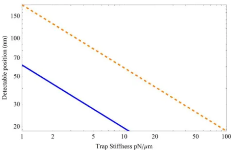
1.3 Detectable position change vs. trap stiness . . . 13

1.4 RNA polymerase step-size measurement . . . 15

1.5 Channel waveguide for particle propulsion . . . 18

1.6 Sorting using counter-propagating elds in a bre . . . 21

1.7 Slot waveguide for particle trapping . . . 22

1.8 Tapered photonic crystal cavity . . . 24

1.9 Photonic crystal cavity trap . . . 25

1.10 Channel waveguide with gold nanopads . . . 30

1.11 Plasmonic nano-aperture array . . . 31

1.12 Self-induced back action in plasmonic apertures . . . 32

1.13 Gold nanoblocks for plasmonic trapping . . . 33

1.14 Bowtie nanoantennas for optical trapping . . . 35

1.15 Plasmonic bottle beams . . . 36

1.16 Polymer embedded gold nanorods . . . 37

1.17 Gold nano rod exciting whispering gallery mode of ultrathin bre . . . 38

1.18 Double-nanohole . . . 39

1.19 NSOM tip with BNA . . . 40

2.1 Refractive index proles of step-index bres . . . 44

xvii

(19)

2.2 Fibre Pulling Rig . . . 50

2.3 Polar plot of dipole scattering. . . 57

2.4 D 2 transitions in rubidium 85 . . . 59

2.5 Optical Molasses Diagram . . . 61

2.6 Zeeman shifting of energy levels and atom trapping . . . 62

2.7 Sketch used in determining the quasi-static approach . . . 64

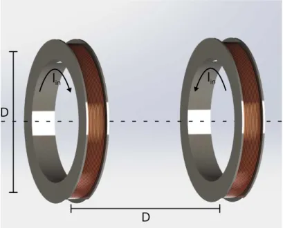
3.1 Diagram of anti-Helmoltz coil . . . 77

3.2 B-eld of an anti-Helmoltz coil . . . 78

3.3 Atom cloud oscillation diagram . . . 79

3.4 Timing scheme for temperature measurement . . . 81

3.5 Flow diagram of the timing scheme used in the temperature measurement . 82 3.6 Sinusoidal t to SPCM output . . . 83

3.7 Oscillation frequency versus phase dierence . . . 84

3.8 CCD image of atom cloud . . . 85

3.9 Oscillation frequency vs. phase dierence for varying pump beam detunings 86 3.10 Atom cloud temperature versus pump probe detuning . . . 87

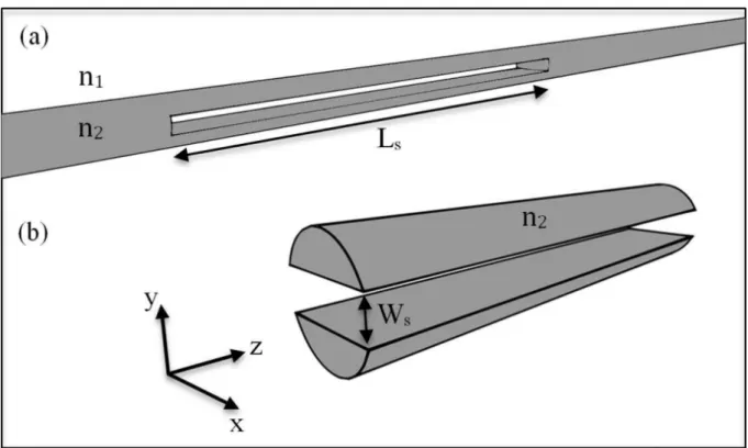
4.1 Schematic of the slotted bre for a vacuum-bre system . . . 92

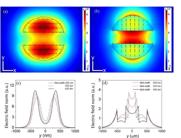
4.2 The electric eld distribution at the slot region of a STOF . . . 94

4.3 Electric eld distribution for the symmetric and anti-symmetric modes . . 95

4.4 Graphic comparing circular sectors and circular segments . . . 96

4.5 Analysis of single- and multi-mode operation regions . . . 96

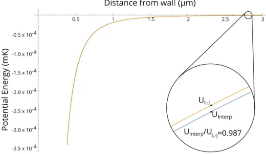
4.6 Normal L-J potential function compared to interpolation QED calculation 98 4.7 Observation of the van der Waals potential near inner STOF surfaces . . . 99

4.8 Combination of blue-detuned and vdW potentials . . . 102

4.9 Surface plot of STOF potential at the slot center . . . 103

4.10 Two-colour trapping potentials for various power combinations . . . 104

4.11 Contributions to the two-colour trap inside and outside the slot section . . 105

(20)

4.12 Eect of power on the trapping potential . . . 106

4.13 Trap depths for varying slot widths . . . 106

4.14 Trap depths at bre surface vs. slot width . . . 107

4.15 Optimisation plots for STOF parameters . . . 108

4.16 First four modes of a nanostrucutured bre . . . 111

4.17 Tapering proles for nanostructured bre . . . 112

4.18 Propagation of rst two excited modes for a tapered slot geometry . . . 113

4.19 FDTD simulation of an untapered and tapered slot . . . 114

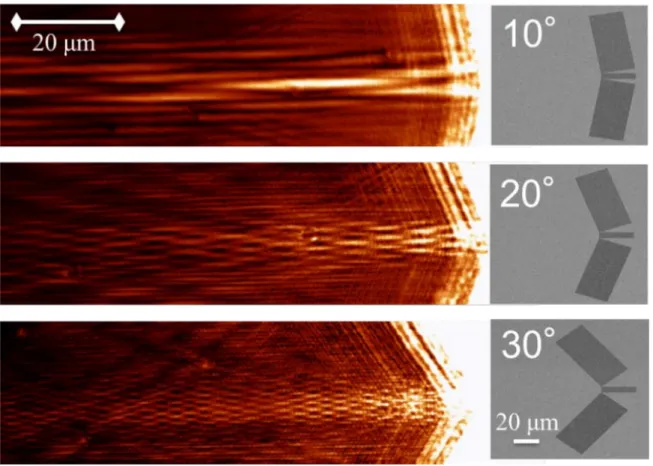
5.1 Slot milling procedure . . . 121

5.2 SEM images of STOFs fabricated using Helios Nanolab TM 650 . . . 125

5.3 SEM images of STOFs fabricated using FIB-SEM Helios G3 UC . . . 126

5.4 3D rendering of a STOF. . . 129

5.5 Fraction of the eld travelling in the core and cladding portions of an ultrathin bre and a segment of circle . . . 131

5.6 Optical setup for trapping 200 nm silica particles with a STOF . . . 132

5.7 FDTD analysis of STOF. . . 135

5.8 Forces on 200 nm particles in a STOF. . . 136

5.9 FDTD simulation for 200 nm particle in a STOF. . . 138

5.10 Interaction force between two particles . . . 139

5.11 Time series of images showing the eect of thermophoresis . . . 141

5.12 Time series and histogram of STOF trap . . . 143

5.13 Trap measurement of slotted tapered optical bre trap . . . 145

5.14 SEM images of uorescent particles . . . 146

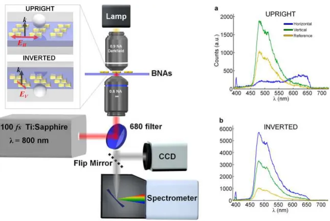
6.1 Elongated gold nanodisk dimers patterned on the surface of an MNF . . . 150

6.2 Elongated gold nanodisk dimer array layout . . . 151

6.3 Layout used for FEM simulation . . . 153

6.4 COMSOL simulation of a gold dimer on silica substrate . . . 154

(21)

6.5 SEM images of the GNR on an ultrathin optical bre taken immediately

after fabrication . . . 155

6.6 SEM images of the GNR on an ultrathin optical bre . . . 156

6.7 SEM images of the GNR on an ultrathin optical bre with defects . . . 156

6.8 Energy-dispersive X-ray spectroscopy measurement on an ultrathin bre plasmonic structure . . . 157

6.9 Absorption spectra for the gold nanodisk array on the surface of an ultra- thin bre . . . 159

6.10 Absorption spectra for the gold nanodisk array on the surface of an ultra- thin bre . . . 159

6.11 Spectrum of light scattered from gold dimer. . . 161

7.1 Schematic of Fresnel microlens traps . . . 163

7.2 Fresnel atom trap potential along central axis . . . 166

7.3 Fresnel atom trap potentials at various z-planes . . . 167

7.4 Diagram and elds from U- and Z- chips . . . 168

7.5 B-eld components for from U- and Z-shaped wires . . . 169

7.6 B-eld along the z-axis for a U-shaped chip for two models . . . 170

7.7 Atom chip design . . . 171

7.8 SEM images of nal devices . . . 173

7.9 Packaged Fresnel microlens atom trap with U- and Z-wires . . . 174

7.10 SEM images of nal devices . . . 175

7.11 Reection spectrum of Device 7 . . . 175

(22)

List of Tables

4.1 Parameters used in trapping potential models. . . 101 4.2 Trap parameters found by varying P r with respect to P b , which was xed

at 30 mW. Values were obtained for a bre width of 1 µ m and a slot width of 350 nm . . . 110 5.1 Parameters for ITO sputter process . . . 123 5.2 Trap stinesses for varying input powers . . . 144 7.1 Device parameters . . . 171

xxi

(23)

Chapter 1

Introduction 1

The idea that particles could be inuenced by the radiation pressure from light has existed as a concept for a very long time; almost 400 years ago Johannes Kepler published a treatise entitled De cometis libelli tres [2], wherein he proposed that solar rays were the cause of the deection of a comet's tail. However, it was not until much later, when James Clerk Maxwell formalised his theory of electromagnetism, that this force could be quantied. In 1906, John Henry Poynting, in relation to the force induced by radiation pressure, stated that even here, so minute is the force, that it only need be taken into account with minute bodies [3]. The next major milestone on the road to harnessing radiation pressure came with the discovery and invention of the laser in 1960 [4].

Just over two decades after the rst operational laser was created, Ashkin et al. [5]

published their seminal paper in 1986 in which they proposed and demonstrated how a laser could be used to trap and manipulate micron and submicron dielectric particles by considering the total conservation of momentum in a light-particle system. The initial design for the optical tweezers, as the design based on Ashkin et al.'s work came to be known, required very few optical components, with the laser source being the most costly. While Ashkin pioneered the work [6], other research groups quickly began to improve upon the design to make it more versatile. Modern optical tweezers allow for

1

This chapter is adapted from M. Daly et al. [1]. M. Daly wrote the majority of the text and S. Nic Chormaic guided the work. All authors reviewed the paper

1

(24)

a high degree of control over several trapping parameters, such as particle location and trap strength. This has been achieved by including components such as acousto-optical deectors, servo-controlled mirror arrays, etc. to create multiple trapping sites and/or to provide control over the particle's motion in the 2D focal plane of the optical tweezers.

Spatial light modulators allow for particle manipulation in the third (axial) direction.

Optical tweezers are capable of performing high resolution measurements when it comes to sensing small displacements of the trapped objects. This property has made the technique of interest to the life sciences where, typically, such small measurements of displacement or force are required, necessitating the use of optical techniques.

In more recent years, the eld of optical trapping has benetted greatly from advances in other optics-related areas. To overcome limitations imposed by the diraction limit of free-space laser beams, the research direction of many optical manipulation groups has shifted to devices that exploit optical near-elds. Optical near-elds, unlike far-elds, can create subdiraction-limited spot sizes. Near-eld devices range from the super- resolution lens as described by Pendry [7] to the use of surface plasmons [8, 9] created by the coherent oscillation of electrons near the boundary of a metal dielectric system. Both of these designs are capable of creating electric eld `hotspots' that can greatly enhance the eld strength locally.

In the introduction to this thesis we seek to outline the current state of the eld

while focussing mainly on methods that can be employed to shift optical trapping into

the nanometre regime through the use of methods and techniques that are not overly

complex in design. The scope of the eld of optical trapping makes a complete review

an almost impossible task. Instead, we touch on many aspects of optical trapping which

relate, in some shape or form, to the research presented in this thesis. The topic of this

thesis is, for the most part, the interaction of light in the evanescent eld of ultrathin

optical bres both in the presence of atoms and particles. In Chapters 3 and 4 some focus

is placed on atomic systems, but the research direction moves towards colloidal particle

systems and the total modication of ultrathin optical bres in Chapters 5 and 6. The

(25)

enhancement of ultrathin bres through surface or bulk modication is a major point in this thesis, and the work performed by other groups, outlined in this section, served as inspiration for many of the approaches we attempted. For more extensive reviews of the biological applications of optical tweezers, or more in-depth discussions about how optical tweezers can be improved by algorithms or diractive elements, the reader's attention is drawn to other works [1012]. Since biological applications are not a core part of this thesis, we do not discuss them in depth.

1.1 Applications

The eld of optical trapping, as with many scientic elds, is motivated by the potential applications that can stem from it. The high degree of control and precision with which one can trap and localise particles using optical tweezers, or other similar trapping systems based on optical forces, is impressive by itself, but it is the ability to then apply these techniques experimentally with incredible resolution that is of interest to scientists.

One of the most common applications of optical tweezers is the strong connement and manipulation of small objects. For example, Waleed et al. [13] used optical tweezers to spatially localise plasmid-coated microparticles that were then optically inserted into MCF-7 cells. The cells were optically perforated using a femtosecond laser to guarantee transfection. In this work, the versatility of the optical tweezers is shown since, not only were the optical tweezers used to manipulate the particle's position, but they were also used to experimentally determine the focal length of various laser sources.

Other work has been done using optical tweezers to measure exceptionally minute

position changes with high resolution. Examples include measuring the step sizes of ki-

nesin proteins along microtubules [14], determining the distance between adjacent base

pairs via determination of the step sizes of DNA polymerase [15]. More recently, unwind-

ing/rewinding dynamics in P-mbriae [16]. Some of these applications will be discussed

in more detail later.

(26)

The application of forces to trapped particles can also be achieved using an optical tweezers and this has been exploited to analyse biological systems. By incorporating opti- cal tweezers with Förster resolved energy transfer (FRET) 2 [17], conformational dynamics of Holliday junctions and the folding dynamics of DNA hairpins have been measured. In- tegrating optical tweezers with other spectroscopic and microscopic techniques is a vital step in the furthering of their applications in the life sciences. This has led to the inte- gration of optical tweezers with techniques such as Raman spectroscopy and stimulated emission depletion (STED) uorescence microscopy [1820]. All of these modications have served to further increase the eectiveness of optical tweezing techniques in many elds.

Moving from manipulating `large', i.e. micron-sized, particles to smaller, nanoscale particles opens up a vast array of applications. The previous examples, which certainly involved the investigation of nanoscale objects such as DNA, were only possible via the use of micron-sized spheres. Much research in this eld is, therefore, focussed on overcoming this size limitation. Eventually, we can expect that trapping small particles, such as bacteria and viruses, will become routine. This would be an excellent achievement for the nanobiology world [21] and some progress in this direction has already been made.

For example, inuenza viruses, of about 100 nm size, have been individually manipulated using optical forces alone [22]. Here, we aim to discuss some of the progress made in these applications, commencing with the introduction of the more well-established techniques in the eld.

1.2 Optical Trapping Regimes

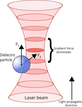
The rst applications of light to trap particles utilised a technique that came to be known as optical tweezing. By employing a tightly focussed Gaussian beam, particles can be trapped near the focus due to the gradient force induced by the momentum exchange

2

The mechanism which describes how energy is transferred between two light-sensitive molecules.

(27)

of photons with the dielectric particles. Ashkin proposed the application of focussed Gaussian beams for both particle [6] and atom trapping [23] using radiation pressure, albeit almost a decade apart. The description of how a particle behaves in a light eld can be understood using dierent models that depend on the particle's size in relation to the wavelength of the light used for trapping. For example, if the particle is large in comparison to the wavelength, a ray-optics approach can be used. Since this chapter focusses on the transition between the micro- and nano-worlds of optical trapping, the details of the ray-optics approach will not be discussed. However, the simple ray-optics explanation does provide a somewhat intuitive model for how trapping occurs and should not be discarded as an invalid approach to describing the optical forces on particles.

1.2.1 Rayleigh Regime

For particles with sizes smaller than or equal to the wavelength of light, an electromagnetic model is required to adequately represent the forces at play in a particlelight system. To assist the reader, we provide a brief description of the forces here, but a more thorough derivation is given in Chapter 2. This solution can range from a more complete theory, which uses the Mie solutions to scattering problems involving spherical or elliptical objects, to a simpler case when the particle size is much smaller than the wavelength of the trapping light and is made from a linear, isotropic material. This allows for the use of the dipole approximation in the calculations. The polarisability of a particle in this case gives rise to a dipole moment, ~ p [24], with

~

p = α ~ E, (1.1)

where E ~ is the electric eld. The electrostatic potential, U , generated by a dipole in an

electric eld is related to this dipole moment via U = − ~ p · E ~ . Hence, the force, F ~ , which

(28)

is the negative gradient of the potential, can be determined

F ~ = −∇ U = ∇ (~ p · E) = ~ α ∇| E ~ | 2 . (1.2) Because of this polarisability dependence, metallic nanoparticles, which, over wave- lengths of interest in particle trapping have a much higher real component of their po- larisability compared to silica or polystyrene particles of the same size, are often used as targets for trapping at the nm-scale since they require the use of lower optical pow- ers. Taking the time average of the eld into account and using the Clausius-Mossotti relationship for a spherical dielectric particle, the so-called gradient force, F ~ grad , a particle feels is nally given as

F ~ grad = 2πn 0 r 3 c

m 2 − 1 m 2 + 2

∇ I(~ r), (1.3)

where r is the particle's radius, c is the speed of light, n 0 is the refractive index of the medium, m is the dielectric contrast, i.e. the ratio of the particle's refractive index to the medium's refractive index, and I (~ r) is the time averaged intensity as a function of position, ~ r . A more in-depth derivation is given in Chapter 2. The dielectric contrast plays a role in the trapping strength of an optical tweezers, but, more interestingly, changing the value of this property can cause the sign of the force to be reversed. If particles of a lower index than their surrounding medium are used, i.e. m < 1 , as is the case for air bubbles in water, the sign of Eqn. 1.3 is seen to change and dierent trapping schemes involving vortex beams are required for trapping [25]. The origin of the term "gradient force" should now be evident from Eqn. 1.3; it is a force that is linearly dependent on the gradient of the intensity and tends to attract particles to regions of higher, or lower, intensity depending on the value of the dielectric constant.

Stable trapping occurs when the net force on a particle is zero and any small displace-

ments from this stable position result in an optical force that resists the motion of the

particle away from this position. Typically, traps with a potential depth greater than the

(29)

thermal limit, i.e. a few k B T , are required for stable trapping, where k B is the Boltzmann constant and T is the particle's temperature in Kelvin. A potential depth of 10k B T is often used as a threshold value for stable particle traps.

To complete the discussion on optical forces, one must also include the scattering force, F ~ scatt , felt by a particle that is being bombarded by a ux of photons of wavenumber k . Under the Rayleigh approximation, along with the Clausius-Mossotti relationship (see Appendix A), this is given as

F ~ scatt = 8πn 0 k 4 r 6 3 c

m 2 − 1 m 2 + 2

2

I(~ r)~ z. (1.4)

Again, these forces are discussed in more detail in Chapter 2, where a full derivation is given.

1.2.2 Mie Solutions and Discrete Dipole Approximation

For particles of intermediate sizes, between that of the ray optics and Rayleigh regimes,

one can apply the Mie solutions [26, 27]. These solutions are the complete solutions to the

Helmholtz equation that take the form of an innite series. The Mie solutions are very

important in this size regime. In the Rayleigh regime, the force scales as the cube of the

particle's radius and this can be shown to be incorrect for larger particles in the ray-optics

regime. The Mie solutions help to bridge this gap between the two regimes, while also

introducing some new phenomena which would otherwise be unnoticed in the theory. In

a paper by Stilgoe et al. [28], a detailed calculation of the trapping forces on particles

of varying radii and refractive indices using dierent numerical apertures is described. A

phenomenon known as a Mie resonance occurs in intermediate-sized particles and this is

more prominent in particles with a higher refractive index contrast between them and the

medium. The presence of Mie resonances strongly changes the trap strength of optical

tweezers, as can be seen from Fig. 1.1 [28], and should be taken into account when

developing tweezers to work at such particle sizes in order to maximise its eectiveness.

(30)

As can be seen in Fig. 1.1(b), interference eects can cause the trap strength to oscillate between trapping and nontrapping regions as the particle size is changed, an eect that is absent in the Rayleigh regime.

If the high accuracy of Mie solutions is not required, but work is being performed at or near the boundary between the Rayleigh and Mie regimes, the dipole can instead be approximated as a discrete sum of dipoles to reduce the errors arising from the single- dipole approximation. Again, a more mathematical description of Mie scattering and the forces at play in light-particle systems is given in Chapter 2.

Figure 1.1: Dependence of trapping force for (a) polystyrene and (b) diamond parti- cles for a xed numerical aperture and particle radii varying from 0 to 3 λ . Note the pronounced interference eects present in the higher refractive index diamond particles.

Reproduced with permission from [28].

(31)

1.2.3 Other Forces

To fully model an optical manipulation system, other forces must be considered. These forces include the Stokes' drag of a particle and the force due to the random Brownian motion. A further discussion of Brownian motion can be found in Section 5.6. The Stokes' drag present in a system can be quite complicated to determine due to the inuence of nearby surfaces. For optical tweezers, Faxen's law [23, 29] is often used to include the inuence of nearby planar surfaces, such as coverslips, in an experiment. Often, these eects can be solved in experiments by modelling the system as a damped harmonic system and calibrating accordingly.

1.3 Optical Tweezers with Free-Space Laser Beams

Optical tweezers epitomise optical trapping. They were the rst devices to be used for optical trapping and were quickly adapted for use in other elds. A discussion of op- tical trapping would, therefore, be incomplete without mentioning optical tweezers. By analysing shortcomings of such devices the motivation behind some of this thesis work is evident. Modular optical tweezers using free-space Gaussian beams are highly versa- tile tools that have high trap stiness when dealing with micron and, to some degree, submicron objects. This is a necessary requirement for precise trapping. They also have incredible resolution with respect to position or force measurements on trapped objects.

It is this resolution that makes optical tweezers invaluable in the life sciences. Applying this type of optical tweezers to the problem of trapping dielectric particles does have two drawbacks when it comes to trapping smaller particles. The rst arises from the diraction limit, which limits the waist size of a Gaussian beam refracted through a lens.

The second drawback is, admittedly, also a side-eect of the diraction limit; particles

of increasingly smaller size require larger gradient forces to trap them. Photons directly

exchange energy with particles via scattering; this force is typically called the scattering

force and, on average, acts in the direction of beam propagation. In the Rayleigh regime,

(32)

the ratio, R , of the magnitude of the gradient force to the scattering force yields an inverse cube dependence on radius. Taking this value at the position of maximal axial intensity gradient yields [5]

R = F grad

F scatt = 3 √ 3 64π 5

n

m

2

−1 m

2

+2

λ 5

r 3 ω 0 2 ≥ 1, (1.5)

where ω 0 is the focal spot size, n is the refractive index of the trapped particle, and m is again the refractive index contrast. This puts an upper limit on the particle size, since the gradient force must dominate. However, the time needed for a particle to be trapped must also be longer than the diusion time out of the trap to ensure ecient trapping. Trapping objects in the nanometre regime requires laser powers which can quickly destroy or denature the samples being trapped. Despite this, optical tweezers systems using focussed Gaussian beams remain invaluable tools.

1.3.1 Optical Tweezers Basics

The term `optical tweezers' has become a term which refers to any optical system that is capable of conning a particle in all three dimensions. The most commonly available system involves the use of free space optical beams to provide a gradient force trap in all directions. Recently, commercial, self-calibrating optical tweezers systems have become available, indicating the rise of interest in the eld.

Free-space optical tweezers exist in many dierent varieties due to their high customis-

ability. As mentioned previously, optical tweezers typically use focussed Gaussian beams,

Fig. 1.2, combined with a mechanism that can deect or otherwise steer the light beam in

and out of the focal plane of the tweezers. Some examples include: galvanometer mounted

mirror arrays to create multiple trapping sites by rapidly moving the trap centre around

the focal plane [30]; holographic optical tweezers that include a spatial light modulator

(SLM) to create dierent trapping patterns; acousto-optic deectors; and even diractive

or polarizing elements. Each variation of optical tweezers has advantages and disadvan-

(33)

Figure 1.2: Schematic of a Gaussian beam optical tweezers. The darker shades of red indicate regions of higher intensity.

tages. For example, SLMs allow for a higher degree of control and customisability, but have typically slow response times [3133]. Both continuous-wave (CW) or pulsed lasers can be used in optical tweezers [34].

The operation of optical tweezers is typically chosen to be in the near-infrared region, primarily because light of wavelength greater than 800 nm is poorly absorbed by most living matter and, as one moves further into the far infrared region, absorption from water molecules becomes an issue [35]. For these reasons, light from an Nd:YAG laser at approximately 1064 nm is commonly used for optical trapping. Optical tweezers are capable of resolving subnanometre motion and measuring pN of force [15, 36].

For optical tweezers in viscous media, the motion of the trapped particle can be well de-

scribed by an overdamped Langevin model, often termed the EinsteinOrnsteinUhlenbeck

theory of Brownian motion [37]. In this overdamped regime, the inertia terms in the

Langevin equation become negligible and the power spectrum of the system can be more

(34)

easily interpreted. To put it simply, the fundamental operational limit for measurements using optical tweezers, or indeed in any of the systems that will be discussed herein, is due to Brownian noise. This noise is always present and, unlike other measurement-based errors such as laser noise, shot noise, imaging errors, etc., it cannot be circumvented. The motion of a particle while trapped in optical tweezers can be described as a harmonic oscillator. Therefore, we may equate the energy of the particle's Brownian motion to the trap's energy using the equipartition theorem, i.e. 1 2 k B T = 1 2 κ h x 2 i [38], where k B is Boltzmann's constant, T is the temperature, κ is the spring constant of the system, and h x 2 i is the particle's mean squared displacement from equilibrium. This can be used to determine the fundamental measurement limit for experiments based on optical tweez- ers. By dening the square root of the mean squared displacement as √

x 2 = p

k B T /κ , the minimum detectable limit can be determined, as shown in Fig. 1.3. Therefore, if one wishes to measure a displacement, the displacement itself should be larger than the Brownian motion. In Fig. 1.3, the two lines correspond to motions which are one (blue solid) and three times (orange dashed) the Brownian motion, with their corresponding de- tection eciencies given in the caption. To measure the trap stiness, a simple Lorentzian function can be tted to the power spectrum, but this gives errors of 1020%. Further studies have shown how to increase the accuracy of such a measurement via modication of the Lorentzian t [39].

The assumption that one can work at this Brownian noise limit is, of course, untrue, as there will always be sources of error that cannot be entirely eradicated. One can, however, work extremely close to this limit. Attempts have been made over the years to reduce noise and increase trapping times in optical tweezers. These approaches range from the use of laser feedback control algorithms to reducing the average laser power and, hence, the associated noise, to the use of interferometric techniques to enhance sensitivity [14, 40].

Although not discussed in detail here, it is worth mentioning that the problems of noise

for optical tweezers in vacuum, such as that associated with optically levitated particles,

(35)

Figure 1.3: Log-log plot of detectable position change versus trap stiness at the thermal limit (blue solid line), which corresponds to 68.5% detection eciency, and three times the thermal limit (orange dashed line), which corresponds to 99.7% detection eciency.

are dierent. Earlier, we discussed an overdamped system, but, in vacuum, the system is underdamped as there is no viscous medium to interact with the trapped particle. A recent demonstration of this comes from Dholakia's group where they optically levitated a particle in vacuum [41]. Aside from the other eects that this has on optical trapping, it also means that the measurement limit now becomes a problem more strongly related to the laser intensity, or, rather, the photon ux. Recoil energy is directly imparted to the particles via interaction with the photons in the laser beam. This is, in many ways, similar to laser cooling of atoms in a magneto-optical trap, where the thermal limit comes not from any interaction with residual gases in the vacuum, but rather from the recoil energy of the laser photons.

An inuential demonstration of optical tweezers was performed in 1993 by Svoboda et

al. [14]. They concluded that kinesin, a type of motor protein found in eukaryotic cells,

moved in 8 nm steps. In this early application of optical tweezers, silica beads were coated

with kinesin in such a way as to allow only a single active molecule per bead. These beads

were then attached to microtubules along which kinesin can move and measurements of

(36)

the step size were made using overlapping beams from a Wollaston prism. Phase objects, such as silica beads, placed in the overlapping region caused varying degrees of ellipticity in the recombined beam and this eect was used to determine ne movements of the objects. This extra step was required to achieve the 8 nm resolution reported and helped show the versatility of optical tweezers in biology.

1.3.2 Dual Beam Optical Tweezers

Single-beam traps are at a disadvantage when compared with dual- or multiple-beam optical tweezers since only one particle can be steered or guided at any given time, un- less Bessel beams or other optics are used to produce multiple trapping planes [42, 43].

Multiple-beam traps can be created numerous ways, such as the time sharing of a single beam using galvonometric mirror arrays, or the splitting of a single beam via polarisation elements to create two individual trapping potentials [44]. A particle suspended in the op- tical gradient of a beam is somewhat decoupled from the environment, but measurements generally require that a second object, which is directly coupled to the environment via some physical stage or mount, be used. This second particle is subject to many forms of external noise, such as stage drift, that often dominate the noise spectrum.

Dual-beam optical tweezers are systems that, eectively, combine two single-beam op- tical tweezers. This allows one to simultaneously trap two objects and perform dierential detection measurements, thereby improving the attainable spatial resolution [36]. Traps of this form existed as early as 1993, although large improvements in stability occured a decade later. Comparing the 8 nm resolution previously obtained [14] to a more recent measurement using a dual-beam trap where a resolution of 3.7 Å was achieved [15], an impressive leap in measurement accuracy can be seen, though admittedly, this jump was not entirely due to the dual-beam conguration itself.

In 2005, base-pair stepping by RNA polymerase was measured and step sizes of 3.7 Å

were distinguishable [15]. This level of high resolution was made possible both through the

use of a dual beam tweezers, as well as isolating the system from external air currents via

(37)

Figure 1.4: RNA polymerase immobilised using a dual beam optical tweezers and

polystyrene beads. T strong and T weak are names given to the traps which refer to them

having high and low spring constants respectively. (b) Noise density for helium enclosure,

blue, and the unenclosed system, red. (c) Steps resolved for a stiy trapped bead moved

in 1 Å increments at 1 Hz. (d) 3.4 Å steps by using a bead-DNA-bead tension of 27 pN

then moving T strong in 3.4 Å increments at 1 Hz. Reproduced with permission [15].

(38)

the use of a helium-lled enclosure. By immobilizing both sides of the RNA polymerase with separate optical tweezers, the noise induced by the motion of the stage was eectively removed. The improved signal-to-noise ratio of dual-beam traps has been quantied by Mott et al. [45]. The system behaves like a three-spring system consisting of two optical tweezers and a DNA strand as the extra spring. Autocorrelations in the motions of two spheres tethered by a DNA strand, as illustrated in Fig. 1.4(a), were measured to determine the 3.7 Å step size. This study showed strong agreement between theory and experiment over the chosen parameter range.

Optical tweezers are also used to apply forces. One such example is the combination of an optical trap with a three color FRET process. In a FRET system, the energy transfer is strongly dependent on the distance between donor and acceptor chromophores [46], which allows one to measure the changes in uorescence during the application of force and hence infer information about the internal dynamics of the system.

Although we only discussed the application of Gaussian beams which have uniform phase-fronts, there have been many successful optical trapping experiments using non- standard beams. Interesting mode congurations, such as Bessel beams, have been used and in more recent years the ability to tailor the phase of light using SLMs or DMDs (deformable mirror devices) has begun to appear in the literature. This is of particular interest to physicists as it allows us to investigate the eects of spin and orbital angular momentum through their eects on dielectric particles, potentially providing us with some new insight into the fundamentals of light. More information can be found in the review paper upon which this chapter is based [1].

1.4 Trapping via Integrated Optics

Trapping nanoparticles, or submicron particles, in subdiraction-limited regimes can be

achieved by using optical near-elds. These can provide high electromagnetic eld gradi-

ents near dielectric surfaces, opening up attractive avenues of research for optical trapping.

(39)

Optical near-elds generally take the form of evanescent elds that decay exponentially from their point of origin. The rst work that made use of the evanescent elds produced by a dielectric channel waveguide was published in 1996 by Kawata and Tani [47]. Here, the authors used only the evanescent eld to propel latex particles of 5.1 µm in diameter along the length of a channeled waveguide at a speed of approximately 5 µm s -1 using only 80 mW of input laser power. While the particles propelled were of a relatively large size, it was the rst work that highlighted the applicability of evanescent elds to particle trapping. Some of the following applications can be classied as tweezers, since they al- low for full 3D connement of the particle, while others only provide connement in fewer dimensions.

The work in this section resonates strongly with the focus of the work in this thesis and the work of the Light-Matter Interactions unit as a whole. Near-eld devices, in the form of ultrathin bres are used in a variety of congurations. This section introduces a number of topics which ultimately led to the development of the devices discussed in later chapters.

1.4.1 Channel Waveguides

Evanescent elds that extend beyond the boundary of light carrying structures, such as waveguides, become more intense as the dimensions of the waveguide approach the wavelength of the guided light or become smaller [48]. This arises due to the wave nature of light that imposes certain boundary conditions on the structures in which they can exist.

Evanescent elds play an indirect role in many plasmonic structures, primarily because

they are used to excite SPPs via the Kretschmann conguration [49]. However, there are

many structures where the evanescent eld can be accessed directly to trap particles. The

evanescent eld from a single beam propagating in an evanescent waveguide provides a

gradient force that attracts particles towards the surface, while a simultaneous scattering

force is applied in the direction of beam propagation. Hence, single-beam evanescent eld

traps are useful for guiding particles along the surface of a waveguide, making them ideal

(40)

Figure 1.5: (a) E-eld intensity plot of the channel waveguide. (b) Particle velocity ver- sus guided power of a 3 µm particle trapped and propelled along a waveguide. Reproduced with permission [50].

for integration with microuidic systems.

An example of a microuidic/evanescent system is described in a paper by Schmidt et al. [50] where they demonstrated how particles could be trapped and propelled using channel waveguides in conjunction with microuidic channels. An illustration of the channel waveguide used is given in Fig. 1.5. This work provided a clear and concise explanation of the physics at play in optouidic systems, as well as displaying the trapping and propulsion of particles of varying size. Similarly, Yang and Erickson [51] have analysed optouidic particle trapping near waveguides. Building on these works, Ng et al. showed that gold colloidal particles as small as 17 nm could be propelled along a channel waveguide [52]. Using branched channel waveguides, or branched microuidic channels, other groups have been able to extend these ideas to particle sorting [53, 54]. The attractiveness of these approaches comes from the fact that microuidic channels and channel waveguides can run parallel to each other, or even inside each other. Simple waveguides can also be arranged such that they produce resonating structures. Lin et al. [55] showed how microparticles can be trapped above a planar silicon microring resonator with large trapping depths of 25 k B T .

There is a current trend in scientic research to encourage the development of lab-

on-a-chip devices. Channel waveguides perfectly t the requirements of a lab-on-a chip

(41)

device as they operate at the correct scale, can be mass produced, and are easily integrated with many existing technologies [56].

1.4.2 Optical Micro-Nanobres

Optical micro- or nanobres (MNFs), or ultrathin optical bres, are optical bres with micron or submicron diameters that do not operate in the weakly guided regime. They are sometimes used to trap particles in their evanescent elds [5760]. MNFs are, generally, manufactured from standard communication-grade optical bres by heating them until they became malleable, at which point a force is applied from either side to elongate and taper the heated region until the central (waist) region of the bre has a diameter less than or equal to 1 µm. A more detailed description of this heat-and-pull procedure can be found in the literature [61, 62]. In contrast, channel waveguides typically need to be grown on a substrate, which allows for complex geometries to be fabricated, but somewhat limits their versatility. For example, some studies in neurobiology require a probe that can reach deep inside tissues in vivo. Very recently, optogenetics has come to the fore in neuroscience and relies heavily on the use of optical bres due to their ability to guide light into areas that are inaccessible using other methods [63]. While these techniques do not directly make use of the evanescent eld or particle trapping, they emphasise the exibility that is introduced once one moves from a platform consisting of rigid channel waveguide structures towards the use of bres. Fibre-based waveguides are capable of trapping and guiding particles as eciently as their substrate-grown counterparts [58, 6466].

The use of a near-eld scanning optical microscope to create a bre optical tweezers (FOT) was realized by Xin et al. [67], and was used to reliably trap micron-sized particles.

Experiments also showed that smaller particles such as yeast, bacteria, and 0.7 µm silica beads could be trapped, albeit with higher laser powers.

To realise a device that operates closer to that of optical tweezers, but with only the

use of the evanescent elds produced by waveguides, one must consider counterpropagat-

ing laser beams [6870]. Here, a standing wave can be formed that produces a potential

(42)

landscape that favours the trapping of particles at certain lattice sites dened by the wavelength of light used. In practice, a standing wave is not entirely necessary for suc- cessfully immobilising particles. Lei et al. [71] showed that, by varying the power of two counterpropagating beams, without the formation of a standing wave, particles with a di- ameter of 710 nm could be transported in either direction along a bre. This was a useful study as it showed that standing waves are not necessary for the controlled guidance of micro- and nanoparticles along a tapered optical bre.

Particle sorting using counterpropagating beams of dierent wavelengths relies on the scattering force's dependence on particle size, refractive index, and the wavelength of light used [72, 73]. Zhang and Li [72] used a subwavelength optical bre with dierent wavelengths of light injected at either end (Fig. 1.6). The dierence in scattering for various particle sizes resulted in the particles being sorted by size.

As is the case for optical tweezers, higher-order modes can be used to trap particles in waveguides. MNFs are an ideal platform for this, as they are capable of supporting many higher-order modes [74, 75], including Bessel-beams [76]. Higher-order mode trapping in straight, channel waveguides has been realised [77], but maintaining these modes in ta- pered bres has proven to be a dicult process due to the ne degree of control required during the fabrication process, although it has been performed successfully using linearly tapered optical nanobres [78]. Adiabaticity requirements impose important shape re- quirements on the taper prole and the dimensions of the bre at the waist must also be considered. These combined conditions require a more complex tapering system [62] than is usually available to research groups. The use of higher-order modes in bres for the purposes of atom trapping has been discussed elsewhere [79, 80].

1.4.3 Slot Waveguides

When two waveguides are placed in close proximity to each other, as is the case in slot

waveguides, the evanescent elds of the two waveguides overlap, producing a region of in-

creased intensity between them [81]. Yang et al. have published a series of papers [82, 83]

(43)

Figure 1.6: (a-d) Visualisation of the dierence in the forces applied to 600 nm and

1000 nm diameter particles due to two dierent wavelengths counter-propagating along

a tapered optical bre. (b) and (d) are simulation results corresponding to (a) and (c)

respectively. (e) A graph of the optical scattering forces on dierent particle sizes due

to dierent wavelengths. Here, the blue line is the scattering from 808 nm light while

the red line shows the scattering from the 1310 nm light, nally, the black line shows the

contribution of both elds to the total scattering force acting on the particle. Reproduced

with permission [72].

(44)

where polystyrene and gold particles are trapped in an optouidic system consisting of a silicon slot waveguide grown on a glass substrate. The small waveguide separation, com- bined with the overlapping evanescent elds, provides a subdiraction-limited trapping potential (Fig. 1.7). The authors were able to trap 75 nm dielectric nanoparticles and λ - DNA molecules using this waveguide system. Lin and Crozier [84] applied this technique to the problem of particle sorting. They used a channel waveguide that ran parallel to a slot waveguide. By introducing a defect, in this case a microsphere that had been fused to the channel waveguide, they were able to `kick' smaller particles out of the potential formed by the channel waveguide and into the potential generated by the slot waveguide, which had a higher eld connement. Initially, 350 nm and 2 µm particles were guided along the channel waveguide. Upon reaching the defect, the 350 nm particles were pushed more than 250 nm away from the channel waveguide where they were then captured by the potential of the slot waveguide.

Figure 1.7: (a) Slot waveguide, (b) electric eld intensity proles for 65 nm polystyrene particles (left), and 100 nm gold particles (right). Reproduced with permission [82].

The use of evanescent devices to trap and manipulate micro- and nanoparticles contin-

ues to be of interest in the scientic community because of their versatility and customis-

(45)

ability. Channel waveguide structures can be incorporated into almost any device at the fabrication stage and are produced using common industrial techniques. This makes their potential uses in commercial products more likely than other, more specialised, devices which are produced by non-scalable, multi-stage techniques. The combination of a slot waveguide with an ultrathin bre was one of the driving motivations behind the work in Chapters 4 and 5.

1.4.4 Photonic Crystal Cavities

With the goal of conning light to subdiraction-limited sizes, many research groups have focussed their interest on photonic crystal (PC) cavities. Photonic crystal structures consist of a waveguide which has been periodically patterned to forbid the transmission of specic wavelengths. If, however, one introduces a defect to this periodic lattice, it is possible to create a region where frequencies that were previously forbidden are now allowed to propagate. By choosing the defect carefully, a cavity can be set up within the crystal structure [85, 86]. If the wave vector of this new cavity mode is chosen so that it is also a conned mode of the waveguide, both lateral and in plane connement is possible [87]. Photonic crystal cavities have some interesting properties that are advantageous for trapping particles. Robinson et al. [88] showed that the modes present in such structures have ultrasmall mode volumes. This leads to extremely high eld gradients over subwavelength dimensions; the connement of the electric eld is comparable to the defect size used to create the cavity.

Particle trapping using photonic crystal cavities was shown to be theoretically possible

by Barth and Benson in 2006 [89]. They concluded that, not only could particles of varying

sizes be trapped with a PC cavity, but the presence of the particles could shift the cavity

resonance, a process known as self-induced back action (SIBA), which is discussed in more

detail in Section 6.3. PC cavity devices have distinct advantages over other evanescent

eld-based devices. For example, Lin et al. [90] showed theoretically that, by tapering the

angle of a PC cavity and including a slot, the gradient force could be signicantly improved

(46)

over that given by a waveguide alone and that a high cavity quality (Q) factor can be maintained. Here the Q factor is a measure of how under-damped a cavity resonance is.

By tapering a PC cavity, as shown in Fig. 1.8, an interesting method of controlling a particle's position was achieved [91]. The angle with which such a device is tapered controls the distance along the z-axis at which dierent wavelengths are reected. This, in turn, produces trapping potentials at dierent locations depending on the frequency of the laser light. Using a tuneable laser source, particles can be moved along the axis of a PC cavity waveguide by gradually varying the wavelength and allowing the trapped particle to follow the changing trap position. Some uncertainity in the particle's position is introduced since the potentials created have multiple minima. However, input powers of 7 mW could, theoretically, trap 50 nm particles stably. PC cavities have also been integrated into optical bres via femtosecond laser ablation processes, as well as composite systems comprising of MNFs in optical contact with external nanostructured gratings [92, 93]. PC cavities oer an eective way of trapping dielectric particles. Recently, van Leest and Caro [94] were able to stably trap single bacteria of two dierent species with an inplane trap stiness of 7.6 pN nm -1 mW -1 .

Figure 1.8: Tapered photonic crystal cavity. zR, zG, and zB are the locations where light of three dierent colours red, green, and blue are reected. Reproduced with permission [91].

Surface traps have also been formed using photonic crystal structures that do not rely

on the introduction of a defect. For example, Jaquay et al. [95] used a photonic crystal

(47)

Figure 1.9: (a) Normalised transmission of the PC cavity system. (b) and (c) are histograms of the data highlighted with the horizontal bars at the left and right of (a), respectively. The histograms of the time series data (red) are given alongside the simulated histogram data (blue). Simulations were performed with a mean particle diameter of 24.8 nm (b) and 30 nm (c). Reproduced with permission [97].

structure where the light was incident perpendicular to the apertures. This produced a

lattice potential that caused particles to congregate and form large self-assembled arrays, a

process that they referred to as light-assisted self-assembly (LATS) [96]. Work performed

by Mirsadeghi and Young [97] using PC cavities has shown that they are a useful tool

for trapping nanoscale particles and providing a means by which the size of the trapped

particle can be determined with nm precision. By introducing a single-mode channel to

a PC structure, particles as small as 24 nm were trapped. Analysis of the transmission

spectra obtained over a number of trapping events was used to determine the mean diam-

eter of the trapped particles by assuming some variance in the particles' polarisabilities,

as shown in Fig. 1.9. As a particle trapping device, PC cavities are promising and their

integration into existing technologies makes them an attractive choice for future progress

in the trapping of particles.

(48)

1.4.5 Microlenses

Microlenses with diameters greater than the wavelength of light can also be used to trap particles in regular arrays. Zhao et al. [98] used arrays of 22 µm microlenses to trap 3.1 µm polymer particles. The relative ease of operation and reliability of such a macroscopic device makes it of interest for applications in the life sciences where high optical alignment may not be available. More recently, a similar device was made using femtosecond laser ablation [99].

1.5 Plasmonic Based Devices

As particle sizes become smaller, problems associated with gradient force trapping arise.

There are two options to enhance trapping at nanometre scales. One can choose to increase the power to further deepen the optical trap, but this is not usually viable as it is advisable to keep powers at a lower level to reduce noise and lessen power-induced damage to the trapped object. This means that one must increase the connement of the laser light by some other means. Plasmonic structures have come to the fore in this size regime.

The eect of surface plasmons on metallic nanostructures of varying designs is being

actively pursued for particle trapping [8, 100]. Nowadays, many research groups have ac-

cess to a wide array of lithography techniques, allowing the creation of arbitrarily shaped

designs. Furthermore, access to nite-element and FDTD software packages allow re-

searchers to model how light interacts with plasmonic materials, photonic crystals, III-V

semiconductors, etc., to a high degree of accuracy. With this arsenal of tools at hand, it

is no surprise that the number of publications in the eld has been rising rapidly in the

last decade.

Figure 1.2: Schematic of a Gaussian beam optical tweezers. The darker shades of red indicate regions of higher intensity.
Figure 1.3: Log-log plot of detectable position change versus trap stiness at the thermal limit (blue solid line), which corresponds to 68.5% detection eciency, and three times the thermal limit (orange dashed line), which corresponds to 99.7% detection ec
Figure 1.14: Au bowtie nanoantenna arrays in upright and inverted conguration and the associated experimental setup
Figure 1.15: Near-eld scanning optical microscopy images of plasmonic bottle beams generated at three dierent grating congurations
+7

参照

関連したドキュメント

On the other hand, when M is complete and π with totally geodesic fibres, we can also obtain from the fact that (M,N,π) is a fibre bundle with the Lie group of isometries of the fibre

S.; On the Solvability of Boundary Value Problems with a Nonlocal Boundary Condition of Integral Form for Multidimentional Hyperbolic Equations, Differential Equations, 2006, vol..

Corollary 5 There exist infinitely many possibilities to extend the derivative x 0 , constructed in Section 9 on Q to all real numbers preserving the Leibnitz

In this paper, we we have illustrated how the modified recursive schemes 2.15 and 2.27 can be used to solve a class of doubly singular two-point boundary value problems 1.1 with Types

Keywords and Phrases: number of limit cycles, generalized Li´enard systems, Dulac-Cherkas functions, systems of linear differential and algebraic equations1. 2001 Mathematical

Section 4 will be devoted to approximation results which allow us to overcome the difficulties which arise on time derivatives while in Section 5, we look at, as an application of

The main problems which are solved in this paper are: how to systematically enumerate combinatorial braid foliations of a disc; how to verify whether a com- binatorial foliation can

We have introduced this section in order to suggest how the rather sophis- ticated stability conditions from the linear cases with delay could be used in interaction with