Thesis for the degree of Doctor of Philosophy
Design of low-voltage and
ultra-low-power analog integrated circuits
by
Zhigang Qin
Graduate School of Electronics Engineering
Saitama Institute of Technology
i
Abstract
In recent years, as a result of the electronic devices in the medical field, the automobile electron system, the military astronautics domain, the smartphones and tablet’s widespread application, the demand for efficient low-power circuits is increasing just as rapidly due to the required battery operations of these handheld devices. Such applications usually require analog and mixed-mode circuits. One of the most important building blocks in analog and mixed-mode circuits is the operational amplifier (op-amp). In analog circuits, the current reference circuit influences on various features of the whole circuit.
The thesis has done the widespread investigation and study to the domestic and foreign technologies of analog low voltage circuits, and analyzed the principles of work, merits and shortcomings of these technologies. It designs a high performance operational amplifier. This article mainly aim at reducing the power consumption to launch the research and design operational amplifier. We develop and fabricate a 0.5-V rail-to-rail op-amp with ultralow-power operation in a 0.18-µm standard complementary metal-oxide-semiconductor (CMOS) process.
unity-ii
gain frequency was 4.0 kHz and phase margin was 56° with a capacitive load of 40 pF. The power consumption was 70 nW including all bias circuits.
iii
Acknowledgements
I would like to express my gratitude to all the people who helped me during the writing of this thesis. My deepest gratitude goes first and foremost to Professor Hirokazu Yoshizawa, my supervisor, for his constant encouragement and guidance. Prof. Yoshizawa taught me the knowledge of electronics and guided me to the world of analog integrated circuits. His constant encouragement and guidance lead me to the place I am standing today. Without his patiently instruction and valuable suggestion, the completion of this thesis would not have been possible. It is impossible to have this thesis completed.
I would like to thank Mr. Akihiro Tanaka, Mr. Kouhei Sakata and Ms. Naomi Takaya for their contribution to the circuit simulation and layout design.
I would like to acknowledge Mr. Hiroo Imamura for helpful advice on the measurements of the operational amplifier too.
Sincere thanks go to Saitama Institute of Technology and University of Science and Technology LiaoNing for the sponsorship of the international exchange programs. It's a great honor to be one of the international exchange student. I would like to thank the Presidents Shunichi Uchiyama and Qiubai Sun for their support.
iv
I would like to express my sincere thanks to Professor Jianting Cao, Professor Matsui Akinori and Professor Yasuhiro Aoki about the correction of my thesis and their precious advice.
And to Professor Zhongchu Wang, Professor Xuedong Zhang, Professor Chongmin Zhang, Professor Yan Chen, Professor Liping Wang, my good friend Mr. XianLong Song and electronic association members of University of Science and Technology LiaoNing, I want to say, thank you so much, from the bottom of my heart.
I would like to express my thanks to the teachers and students that I met in Saitama Institute of Technology and University, appreciate all your encouragement and support, study abroad is not easy as what I was thinking, even though it has a lot of challenges in different ways, but the experience enriched my life and fill with hope. Thanks for every single person I have met in the past several years while I am study in Japan, especially Xing Liu, Xinmao Fu and the others that we met in Ju laboratory. We fight though the hard time, laugh together for the happiness, makes studying and living in another country plenty more easier, find happy easy like I was at home.
This work is supported by VLSI Design and Education Center (VDEC), the University of Tokyo in collaboration with Synopsys Inc, Candence Inc, Mentor Graphics Inc, and Rohm Corporation.
v
vi
TABLE OF CONTENTS
Abstract ……….……..…ⅰ Acknowledgements ...………...….…………ⅲ 1. Introduction ………1 1.1 Thesis Introduction ……….………..……1 1.2 Thesis Outline ……….………...………...22. Fundamentalsof Analog Design and CMOS Integrated-Circuit Technology ………..3
2.1 Introduction ………...3
2.2 MOS transistor structure ………...3
2.3 Weak Inversion in CMOS Transistors ……….……..…………4
2.4 Current Source and Current Mirrors………..………....5
2.5 Cascode stage ...……….………8
2.6 Folded cascode op-amp ……….………8
3. Rail-to-Rail Operational Amplifier Using a Cross-Coupled Output Stage ……..…..10
3.1 Early Work and Applications ………..………...10
3.2 Proposed circuit ………..…………..……..……...12
3.2.1 Input stage ………..………..……..……..……...12
3.2.2 Cross-coupled output stage………..………..……...14
3.2.3 Reference-Current generation Circuit……….……..…………...16
3.3 Simulation Results ………. …………..……..……..……...17
3.4 Integrated Circuit Layout and Experimental Results ………...30
4. Ultra-Low-Voltage and Ultra-Low Current Reference Circuit ………...37
vii
4.2 Proposed low-voltage current reference circuit ………...42
4.3 Simulation Results and Layout………...46
5. Conclusions ………...49
Design of ultra-low-voltage and ultra-low-power
analog integrated circuits
Chapter 1 Introduction
1.1 Thesis Introduction
Microelectronic technique, electronic technology and computer technology with the close relations of mutually permeating, supporting and promoting each other, have gotten development at high speed. Analog and digital circuits with ultra-low power consumption can be widely used in many areas of applications. With the continuous development of deep-submicron technology, the voltage of power supply becomes lower and lower. It is very essential to study the design of low voltage and low power reference resource based on standard CMOS process [1].
At present, the low voltage low power CMOS analog integrated circuit and the current mode circuit with a great deal of merits are concerned very much by theory researchers and project engineers for VLSI technology.
2
nano-power rail-to-rail input stage CMOS operational amplifier and a ultra-low current reference circuit are described.
1.2 Thesis Outline
Chapter 2 of this thesis describes fundamentals of CMOS analog circuit design. It begins with a description of device in analog and digital CMOS processes. Then, Transistors in their weak-inversion saturation regions are introduced. In addition, the current sources and current mirrors are described.
Chapter 3 describes the background of this research work. Early work and applications are also discussed. Then, we proposed a rail-to-rail op-amp circuit, and described of simulation and experimental results.
In Chapter 4 the concept of ultra-low-voltage and ultra-low current reference circuit is introduced, and simulation results obtained from the new circuit are also shown.
3 Chapter 2
Fundamentals of Analog Design and CMOS Integrated-Circuit Technology
In this chapter, devices in analog and digital CMOS processes are described. Then, transistors in their weak-inversion saturation regions are introduced.
2.1 Introduction
Integrated circuit design is separated into two major categories: analog and digital. An analog signal is a signal that is defined over a continuous range of time and a continuous range of amplitudes. Circuit design is the creative process of developing a circuit that solves a particular problem. Design can be better understood by comparing it to analysis [2].
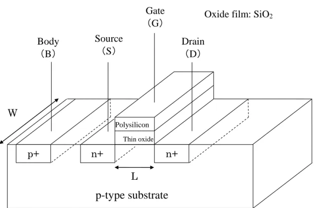
2.2 MOS transistor structure
4
n+
n+
p-type substrate
Thin oxide PolysiliconSource
(S)
Gate
(G)
Drain
(D)
p+
Body
(B)
L
W
Oxide film: SiO
2Fig. 2.1. Structure of a MOS device.
2.3 Weak Inversion in CMOS Transistors
The device operates in weak inversion when gate-source voltages less than the extrapolated threshold voltage VT but high enough to create a depletion region at the surface of the silicon.
In the weak inversion region, the drain current is
ID = 𝐼𝐼0𝑊𝑊𝐿𝐿 𝑒𝑒𝑒𝑒𝑒𝑒{𝑞𝑞(𝑉𝑉𝑛𝑛𝑛𝑛𝑛𝑛𝐺𝐺𝐺𝐺−𝑉𝑉𝑇𝑇)} �1 − exp �−𝑞𝑞𝑉𝑉𝑛𝑛𝑛𝑛𝐷𝐷𝐺𝐺��, (2.1)
5 2.4 Current Sink and Current Mirrors
Current sink is realized by an NMOS transistor as shown in Fig. 2.2. And its current-voltage characteristic is shown in Fig. 2.3. The voltage across the current sink must be larger than Vmin in order for the current sink to perform properly.
A simple CMOS current mirror shown in Fig. 2.4. In analog circuits, the design of current sources is based on “copying” currents from a reference, with the assumption that one precisely-defined current source is already available [1].
Iout VDS ID 0 Linear region
Fig. 2.3. Current-voltage characteristics (ID-VDS) [2].
Saturation region
VGS-VT
= VDS sat
Fig. 2.2. Current sink[3]. VOUT (min) =VBIAS–VT
IOUT
VBIAS
+
6
Fig. 2.4. A simple CMOS current mirror [1].
IOUT IREF M1 M2 VGS + ‐ 1 1 L W 2 2 L W VSS=0
The drain-gate voltage of M1 is zero. The transistor M1 operates in the saturation or active region if the threshold is positive.
M1 and M2 operate in the saturation region. Their currents are given by
(
1)
2 1 1 OX ( ) 1 C 2 1 DS TN GS n REF V V V L W I = µ − +λ , (2.2) ( 2) 2 2 2 OX ( ) 1 C 2 1 DS TN GS n OUT V V V L W I = µ − +λ . (2.3)In the most general case, the ratio of IOUT to IREF is
(
)
(
1)
1 1 2 2 2 1 1 DS DS REF OUT V L W V L W I I λ λ + + = . (2.4)Neglecting channel-length modulation, we can write
7
Consequently,the ratio of IOUT/IREF is given by the ratio of device dimensions.
8 2.5 Cascode stage
The cascade of a common-source (CS) stage and a common-stage (CG) is called a “cascode” topology (The term cascode is believed to be acronym for “cascade triodes,” possibly invented in vacuum tube days.) [1]. Fig. 2.5 shows a cascode stage. It provides a high output impedance and reduces the effect of the Miller capacitance.
V
DD M1 M2 R VOUT VIN Gm2 VIN VbiasFig. 2.5. Cascode stage.
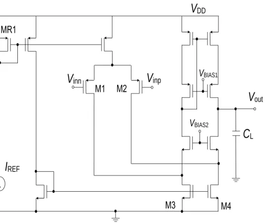
2.6 Folded-cascode op-amp
9
V
innV
inpI
REFV
BIAS2V
outV
DDC
LMR1
M1 M2
M3
M4
V
BIAS110 Chapter 3
Rail-to-Rail Operational Amplifier Using a Cross-Coupled Output Stage
3.1 Early Work and Applications
For more than a decade, low-voltage op-amps which operate with a supply voltage of 1V or below have been investigated [5-9]. Blalock proposed a body-driven input stage for a 1-V rail-to-rail op-amp [5], and Chatterjee realized a 0.5-V op-amp by using the body-driven technique [6]. However, the input impedance of these op-amps drop significantly when the pn junction of an input PMOS transistor, which consists of the source (p-type) and the body (n-type), is forward-biased. The circuit of [6] may get into the latch-up state when the supply voltage exceeds 0.7 V.
Stockstad proposed a buffered body-driven technique and realized a 0.9-V rail-to-rail op-amp [7], which operates up to 5.5 V. The input impedance is as high as that of a typical gate-driven CMOS op-amp. However, this circuit uses depletion-type NMOS transistors, which are usually not available in standard CMOS processes.
11 VDD Vout IS1 VDD inn inp C2 0.8p IS2 inn inp C1 0.8p M3 M1 M4 M6 M8 M7 M5 M2 M9
Fig. 3.1. Rail-to-Rail op-amp with a standard CMOS technology [9].
12 3.2 Proposed circuit
In this brief, we describe a 0.5-V rail-to-rail CMOS op-amp. It has a large common-mode input range, which comprises a cross-coupled output stage to increase both the gain of the op-amp and drivability for a capacitive load. It can be realized in a standard CMOS process. The performance of the op-amp has been verified by HSPICE simulations. We have fabricated the op-amp using a standard CMOS process, and described the experimental results.
3.2.1 Input stage
Fig. 3.2 shows the proposed rail-to-rail op-amp. Unlike the circuit of [9], the gates of M3 and M7 are not connected to their drains. Therefore, VDS3 and VSD7
can be as small as 100 mV while keeping these MOS transistors in their weak-inversion saturation regions.
In the circuit of Fig. 3.1, the minimum common-mode input voltage, Vcmin (min), is
Vcmin (min) = VGS3 + VSD1 – VSG1 > 0 V. (3.1)
Assuming VGS3 = VSG1, Vcmin (min) is higher than 0 V. It means that the
common-mode input range does not cover the ground (0 V) in this structure. In the circuit of Fig. 3.2, on the other hand, the minimum common-mode input voltage is
Vcmin (min) = VDS3 + VSD1 – VSG1 < 0 V. (3.2)
Assuming VDS3 = VSD1, Vcmin (min) can be lower than 0 V. Therefore, the
13
The maximum common-mode input voltage, Vcmin (max), in the circuit of Fig. 3.1 is
Vcmin (max) = VDD – VSG7 – VDS5 + VGS5 < VDD. (3.3)
In the circuit of Fig. 3.2, on the other hand, it is
Vcmin (max) = VDD – VSD7 – VDS5 + VGS5 > VDD. (3.4)
Additionally the proposed circuit has a cascode structure in the first stage and a high voltage gain is expected.
Each MOSFET has been designed to have a gate-to-source voltage (VGS) of
0.2 V. It is obvious that these MOSFETs operate in their subthreshold regions. Their drain-to-source voltages are kept more than 100 mV so that they stay in their saturation regions.
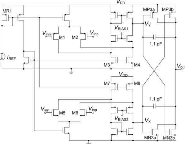
Vinn Vinp IREF VBIAS1 VX VY MN3a MN3b MP3a MP3b VBIAS2 Vinn Vinp Vout VDD VDD 1.1 pF 1.1 pF MR1 M1 M2 M3 M4 M5 M6 M7 M8
14 3.2.2 Cross-coupled output stage
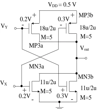
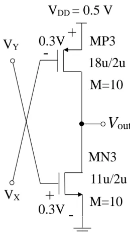
Fig. 3.3(a) shows a conventional common-source output stage. We assume here that both PMOS transistor MP3 and NMOS transistor MN3 comprise 10 unit transistors in parallel.
Fig. 3.3(b) shows our novel cross-coupled output stage [10]. Essentially, the PMOS transistor MP3 in Fig. 3.3(a) is divided in half and shown in Fig. 3.3(b) as MP3a and MP3b. Both MP3a and MP3b comprise five unit transistors in parallel. Similarly, NMOS transistor MN3 in Fig. 3.3(a) is also divided in half, as shown in Fig. 3.3(b) as MN3a and MN3b. Both MN3a and MN3b comprise five unit transistors in parallel. Therefore, the silicon area is unchanged in our new design.
In the following explanation, we assume that VDD is 0.5 V. The gate terminal
of MP3b is connected to the gate of MN3a, and the gate terminal of MN3b is connected to the gate of MP3a. For example, if VSG of MP3a is set to 0.2 V, then
VGS of MN3b is 0.3 V. Furthermore, if VGS of MN3a is set to 0.2 V, then VSG
of MP3b is 0.3 V. Because VGS of MN3b and VSG of MP3b are larger than those
of the conventional common-source output stage shown in Fig. 3.3(a), the transconductances of these MOSFETs increase. Conversely, VGS of MN3a and
VSG of MP3a are each 0.2 V that is similar to VGS or VSG of MOSFETs in the
15 Vout VX VY 0.2V
+
-
0.2V+
-
VDD = 0.5 V M=10 M=10 18u/2u 11u/2u MN3 MP3Fig. 3.3 (a). Conventional common-source output stage [18].
Fig. 3.3 (b). Proposed cross-coupled output stage.
16
is connected to VY, and the gate terminal of MP3 is connected to VX.
Although this structure increases the transconductance of the output stage, the quiescent current also increases significantly.
V
out
V
XV
Y0.3V
+
-
0.3V
+
-
V
DD= 0.5 V
M=10
M=10
18u/2u
11u/2u
MN3
MP3
Fig. 3.3 (c). shows a fully cross-coupled output stage. The gate terminal of MN3.
As a conclusion, we expect that the cross-coupled output stage shown in Fig. 3.3(b) is the most useful among them. It increases the transconductance of MOSFETs of the output stage and enhances the gain of the op-amp and drivability for a capacitive load with moderate current consumption.
3.2.3 Reference-current generation circuit
17
circuit [10] to generate a reference current of 2 nA. Without using a resistor, a supply-voltage-independent current-reference circuit is realized.
MIREF in Fig. 3.4 works as a current source (IREF) in Fig. 3.2. MR2, MR3, MR4,
MR5 and MR6 form the supply-independent bias circuit. Unlike a conventional bias circuit in which a resistor is used, an NMOS transistor MR6 is used for the resistor-free circuit [10].
V
DD IREF MIREF MR1 MR2 MR3 MR4 MR5 MR6Fig. 3.4. Reference-current generation circuit [10].
3.3 Simulation Results
We have run HSPICE simulations for the proposed circuit shown in Fig. 3.2 using SPICE parameters for a standard 0.18-µm CMOS process with a supply voltage of 0.5 V. Bias circuits for VBIAS1 and VBIAS2 (not shown in Fig. .2) are
18
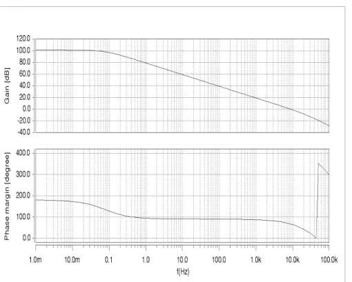
Fig. 3.5. Gain (above) and phase margin (below).
Fig. 3.5 shows the gain and phase margin at the common-mode input voltage of 0.25 V. The DC gain of the proposed op-amp is 101 dB, the unity-gain frequency is 8.2 kHz, and the phase margin is 50 degree with a load capacitance of 40 pF. The power consumption is 85 nW for the whole circuit including bias circuits.
19
Fig. 3.6. Voltage difference between the input and output in a voltage-follower configuration.
20 (a)
(b)
Fig. 3.7. Process corner simulations. (a) DC gain. (b) Unity-gain frequency.
0 15 30 45 60 75 90 105 120 FF FS TYP SF SS D C g a in [ dB ]
with internal current source with ideal 2-nA current source
0 5 10 15 20 25 30 FF FS TYP SF SS U ni ty -g a in fr eq ue nc y [ kH z]
with internal current source
21 (c)
Fig. 3.7. Process corner simulations. (c) Phase margin.
Fig. 3.8 shows the supply-voltage dependence of the total current consumption. For comparison, circuits using output stages of Figs. 2a and 2c are also shown. In the proposed circuit using the cross-coupled output stage of Fig. 2b, the total current increases to 774 nA at 0.6 V. In Fig. 2c, the total current was 1.34 µA at 0.6 V (It was 282 nA at 0.5 V). The supply-voltage dependence of total current consumption is a shortcoming of the cross-coupled output stage. However, the proposed circuit was developed for ultra-low voltage applications, such as 0.5 V, and is not suitable for a supply voltage larger than 0.5 V.
0 10 20 30 40 50 60 70 80 FF FS TYP SF SS P ha se m a rg in [º ]
22
Fig. 3.8. Supply-voltage dependence of total current consumption.
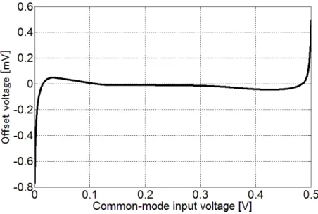
Fig. 3.9 shows the DC gain with the common-mode input voltage. The proposed circuit has a DC gain of more than 80 dB for common-mode input voltages from 40 mV to 400 mV, and more than 60 dB from 32 mV to 467 mV. For comparison, the DC gain of an op-amp without the cross-coupled output stage (with a common-source output stage instead) is also shown in Fig. 3.9.
0 0.2 0.4 0.6 0.8 1 1.2 1.4 1.6 0.5 0.52 0.54 0.56 0.58 0.6 T o ta l cu rren t [µ A] VDD[V]
with an output stage of Fig. 2a with an output stage of Fig. 2b with an output stage of Fig. 2c
23
Fig. 3.9. DC gain and common-mode input voltage.
The transconductance of the input stage is shown in Fig. 3.10. Since the input stage consists of a PMOS pair and an NMOS pair, the total transconductance of the input stage depends on the common-mode input voltage. This is a subject for future. 0 20 40 60 80 100 120 0 50 100 150 200 250 300 350 400 450 500 D C g a in [ dB ]
Common-mode input voltage [mV]
with a cross-coupled output stage (Fig.2)
with a common-source output stage (Fig. 10)
24
Fig. 3.10. Transconductance and the common-mode input voltage.
Common-mode rejection ratio (CMRR) is shown in Fig. 3.11. CMRR of 90 dB is obtained for low frequencies.
Figure of merit (FoM) is calculated using the equation described below,
total L I C UGF FoM = ⋅ , (3.5)
where UGF is the unity-gain frequency, CL is the load capacitance, and Itotal
25
Fig. 3.11. Common-mode rejection ratio (CMRR).
Maximum sink current and source current at a supply voltage of 0.5 V are 52 µA and 23 µA, respectively.
26 Vinn Vinp IREF VBIAS1 VX VY MN3 MP3 VBIAS2 Vinn Vinp Vout VDD VDD 1.1 pF 1.1 pF MR1 M1 M2 M3 M4 M5 M6 M7 M8
Fig. 3.12. Rail-to-rail op-amp with a common-source output stage.
27
Fig. 3.13 shows simulation results of the current reference circuit used in the op-amp. The reference current was 2 nA at a supply voltage of 0.5 V. Because the reference current is not constant at a supply voltage of 0.5 V, the reference current circuit must be improved for future.
28
Fig. 3.14 shows process variations of the reference current used in the op-amp. In Fig. 3.14, the first symbol represents the NMOS condition and the second symbol represents the PMOS condition. The symbol F means fast and S means slow. T represents typical. For example, FS indicates a combination of fast NMOS and slow PMOS. At a supply voltage of 0.5V, the reference current was affected a lot by process conditions. The robust design of the 2-nA reference current circuit which operates at 0.5 V is our future task.
Fig. 3.14. Reference currents for process variations.
0 1 2 3 4 5 6 0 0.1 0.2 0.3 0.4 0.5 0.6 0.7 0.8 0.9 1 1.1 1.2 1.3 1.4 1.5 1.6 1.7 1.8 1.9 R ef er en ce cu rr en t [ n A ] Supply voltage [V]
Process corner simulation
29
Table I summarizes simulation results of the proposed circuit with those of related circuits.
TABLE I SUMMARY OF SIMULATION/EXPERIMENTAL RESULTS [16]
[1]* [2]* [3]* [4]* [5]** This work with a cross-coupled output stage**
This work with a common-source output stage** Supply voltage [V] 1.0 0.5 0.9 0.5 0.4 0.5 0.5
DC gain [dB] 49 62 79 62 63 101 92
Unity-gain frequency [kHz] 1,300 10,000 5.6 102 5.0 8.2/8.6 8.3 Load capacitance CL [pF] 22 20 12 20 N/A 40/20 5
Phase margin [degree] 57 N/A 62 52 N/A 50/59 49 Supply current [µA] 300 150 0.5 3.0 0.02 0.17 0.057
Power [µW] 300 75 0.45 1.5 0.008 0.085 0.029 CMRR (at DC) [dB] 56** N/A 59 N/A N/A 90 90 Figure of Merit [MHz⋅pF/mA] 100 1330 130 680 N/A 1930/1010 730
30
3.4 Integrated Circuit Layout and Experimental Results
We fabricated the proposed op-amp shown in Fig. 3.2 in a standard 0.18-µm CMOS process. The layout and die photograph of the op-amp are shown in Figs. 3.15 and 3.16, respectively. Excluding the 2-nA current reference circuit, the die area for the op-amp was 0.018 mm2; similarly, the die area of the 2-nA current
reference circuit was 0.018 mm2.
31
Fig. 3.16. Die photograph of the op-amp [18].
32
Fig. 3.17. Measured rail-to-rail input (yellow line) and output (blue line) waveforms with a 0.5-V supply voltage [18].
33
(a)
(b)
Fig. 3.18. Measured open-loop frequency response. (a) Gain. (b) Phase [18].
34
Fig. 3.19 shows the DC gains and common-mode input voltages. For common-mode input voltages at 50 and 450 mV (i.e., at 50 mV from each supply rail), the DC gains of more than 40 dB were obtained.
Fig. 3.19. Measured DC gain and common-mode input voltage [18].
We measured the common-mode rejection ratio (CMRR) and power supply rejection ratio (PSRR) of the proposed circuit shown in Fig. 3.2. With a supply voltage of 0.5 V, CMRR was 55 dB for the common-mode input voltages of 0 and 0.5 V. PSRR was 52 dB for the supply voltages ranging 0.5−1.0 V.
-0.3 2.2 10.0 20.1 29.5 40.2 56.8 63.3 72.0 77.3 72.7 64.7 56.2 40.7 31.0 25.0 15.2 7.1 -1.7 -10 0 10 20 30 40 50 60 70 80 90 0 50 100 150 200 250 300 350 400 450 500 D C g a in [ dB ]
35
Furthermore, the measured offset voltages were −0.8, −4.4, −6.2, and −7.8 mV (four samples). And the slew rate of the op-amp was 2 V/ms for both the rise and fall.
The figure of merit (FoM) of the op-amp was calculated using the conventional equation described as follows [4]:
total L I C UGF FoM1= ⋅ , (3.6) where UGF is the unity-gain frequency, CL is the load capacitance, and Itotal is the current consumed in the entire circuit. Thus, the FoM1 of our proposed circuit (including all bias and reference circuits) was 1143 with a load capacitance of 40 pF. Here, to include the effect of the phase margin for fair comparison, we also adopted another FoM equation described as follows [12]:
° ⋅ ⋅ = 60 tan tan 2 M total L I C UGF FoM φ , (3.7) where φM is the phase margin of the op-amp. Then, the FoM2 of our circuit
was 978.
TABLE II SUMMARY OF SIMULATION AND EXPERIMENTAL RESULTS [18]
Simulation results Experimental results Supply voltage [V] 0.5 0.5 DC gain [dB] 101 77 Unity-gain frequency [kHz] 8.2 4.0 Load capacitance [pF] 40 40 Phase margin [˚] 50 56
Supply current [nA] 170 140
Power [nW] 85 70
FoM1 [MHz pF/mA] 1929 1143
36
Table II summarizes the simulation and experimental results of the proposed op-amp. Table III summarizes the experimental results of the proposed circuit and those of the previously reported low-voltage op-amps. Our op-amp shows a large FoM, occupies a relatively small chip area, and has a rail-to-rail input/output feature operating with a supply voltage of 0.5 V. Moreover, high FoM values were obtained in [4] and [8]. However, these two op-amps do not have the rail-to-rail input/output feature. With a supply voltage of 0.5 V or less, the rail-to-rail operation is only available in [6], [9], and this work.
TABLE III SUMMARY OF EXPERIMENTAL RESULTS AS COMPARED TO PREVIOUSLY
REPORTED LOW-VOLTAGE OP-AMPS [18] This work [1] [2] [3] [4] [13] [14] [15] Supply voltage [V] 0.5 1.0 0.5 0.9 0.5 1.0 1.0 0.25 Technology 0.18 µm 2 µm 0.18 µm 2.5 µm 0.18 µm 0.35 µm 0.35 µm 0.13 µm DC gain [dB] 77 49 62 79 62 76 88 60 Unity-gain frequency [kHz] 4.0 1,300 10,000 5.6 102 8,100 11,670 1.9 Load capacitance [pF] 40 22 20 12 20 17 15 15
Phase margin [˚] 56 57 N/A 62 52 N/A 66 53
Supply current [µA] 0.14 300 150 0.5 3.0 358 197 0.072
Power [µW] 0.07 300 75 0.45 1.5 358 197 0.018
Slew rate (rise) [V/µs] 0.002 0.7 2 N/A 0.035 2.74 2.53 0.0006 Slew rate (fall) [V/µs] 0.002 1.6 N/A N/A 0.032 5.02 1.37 0.0008 CMRR [dB] 55 @ DC N/A 75 @ 5 kHz 59 @ DC N/A 71 @ DC 40 @ DC N/A
PSRR [dB] 52 @ DC 61 @ 10 kHz 81 @ 5 kHz N/A N/A 45 @ DC 40 @ DC N/A Area [mm2] 0.036 1.514 0.017 0.5 0.006 0.053 0.157 0.083
FoM1 [MHz pF/mA] 1,143 95 1,334 134 680 385 889 392
FoM2 [MHz pF/mA] 978 85 – 146 503 – 1,152 303
37 Chapter 4
Ultra-Low-Voltage and Ultra-Low Current Reference Circuit
In analog circuits, the current reference circuit influences on various features of the whole circuit. A resistor-less current reference circuit for ultra-low-voltage and ultra-low current circuits is proposed in this chapter.
This chapter describes a 0.6-V current reference circuit for use in ultra-low-power applications. In a conventional beta multiplier current reference circuit, a MOSFET that operates in the strong inversion and triode regions is used as a resistor. Our proposed circuit provides a forward body-biasing for the MOSFET to lower its threshold voltage and make it operate in its strong inversion region even at a very low supply voltage of 0.6 V. We ran simulations using SPICE parameters for a 0.18-µm standard CMOS process.
38 4.1 Early Work and Applications
As the requirement about battery operations of handheld devices increases, the digital increases which about portable electronic devices, such as smart phones and tablets. And the demand for efficient low-power circuits increases rapidly. The current reference circuit is one of the most important parts in analog and mixed circuit systems. It generates reference current, which is used for op-amps, oscillators, phase-locked loops and, A/D and D/A converters, etc [10], [20-21].
CMOS analog integrated circuit, operated in the weak region, with has been draw much attention because of its potential in low operating voltage and low power consumption. The dedicated special circuit structure in order to the special requirements of analog integrated circuits.
Low-voltage, low-current reference circuits have been reported [19-35]. Circuits of ref [20-29] operate at a supply voltage over 1 V. Circuits of refs. [30-35] operate at a supply voltage of 1 V or less, however reference currents of refs. [31, 33] are over 50 nA. Circuits with reference currents of only several nano-amperes have also been reported [24, 29, 30].
A conventional current reference circuit (Beta-multiplier current reference circuit [20]) is show in Fig. 4.1. P-channel MOSFETS M1 and M2 forms a current mirror. When N-channel MOSFETS M3 and M4 operate in weak inversion region, the source voltage of M3 is given by:
39
where UT = kT/q is the thermal voltage, and SM1–SM4 are aspect ratios of M1 –
M4 [20]. VSM3 is equal to the voltage difference across the resistor R. The area of the resistor R becomes very large. The reference current IREF is therefore given
by the following equation:
𝐼𝐼REF = 𝑈𝑈𝑅𝑅𝑇𝑇ln (𝑆𝑆𝑆𝑆𝑀𝑀4𝑀𝑀3𝑆𝑆𝑆𝑆𝑀𝑀2𝑀𝑀1) (4.2)
V
DDI
REFM1
M2
M3
M4
R
Fig. 4.1. Beta-multiplier current reference circuit [20].
A nano-ampere order of magnitude of the current reference circuit as show in fig. 4.1 needs hundreds of mega-ohm resistor elements, and it is hard to realize it in integrated circuits.
40
other word, a circuit was proposed in which the resistor R was replaced by an NMOS operating in strong inversion region and ohmic region. NMOS transistor M5 operates in its strong inversion and triode region. N-channel MOSFETs M3 and M4 operate in weak inversion. A chip area can be made smaller than a circuit using resistive elements.
However, the output voltage is 0.5 V of one unit solar cell, under such a low supply voltage, it is difficult to realize that the NMOS transistor M5 works in strong inversion region.
V
DDI
REFM1
M2
M3
M4
M5
M6
M7
41
A 0.5-V operational amplifier was been proposed [18]. That paper used the Oguey bias circuit to generate a reference current of 2 nA. Without using a resistor, a supply-voltage-independent current-reference circuit is realized. The current reference circuit takes the place of the MOS transistor resistance element which works on the weak inversion region.
However, at a supply voltage of 0.5V or 0.6 V, NMOS transistor M5 operates in its weak inversion region, unless a special process with a low threshold voltage is used. The resistance linearity of this NMOS transistor then becomes worse than in the strong inversion region.
In the weak inversion region, the drain current of the NMOS transistor M5 is given by the following equation:
ID = 𝐼𝐼0𝑊𝑊𝐿𝐿 𝑒𝑒𝑒𝑒𝑒𝑒{𝑞𝑞(𝑉𝑉𝑛𝑛𝑛𝑛𝑛𝑛𝐺𝐺𝐺𝐺−𝑉𝑉𝑇𝑇)} �1 − exp �−𝑞𝑞𝑉𝑉𝑛𝑛𝑛𝑛𝐷𝐷𝐺𝐺��, (4.3)
where 𝐼𝐼o is the process-dependent parameter, and n is the slope factor. The drain conductance is given as follows:
𝑔𝑔𝑑𝑑 = 𝜕𝜕𝐼𝐼𝐷𝐷 𝜕𝜕𝑉𝑉𝐷𝐷𝐺𝐺= 𝑞𝑞 𝑛𝑛𝑛𝑛𝐼𝐼0 𝑊𝑊 𝐿𝐿 𝑒𝑒𝑒𝑒𝑒𝑒{ 𝑞𝑞(𝑉𝑉𝐺𝐺𝐺𝐺−𝑉𝑉𝑇𝑇−𝑛𝑛𝑉𝑉𝐷𝐷𝐺𝐺) 𝑛𝑛𝑛𝑛𝑛𝑛 }. (4.4)
Therefore, the MOSFET drain resistance can be expressed as following: 𝑅𝑅 =𝜕𝜕𝑉𝑉𝐷𝐷𝐺𝐺 𝜕𝜕𝐼𝐼𝐷𝐷 = 𝑛𝑛𝑛𝑛 𝑞𝑞 1 𝐼𝐼0 𝐿𝐿 𝑊𝑊𝑒𝑒𝑒𝑒𝑒𝑒{ −𝑞𝑞(𝑉𝑉𝐺𝐺𝐺𝐺−𝑉𝑉𝑇𝑇−𝑛𝑛𝑉𝑉𝐷𝐷𝐺𝐺) 𝑛𝑛𝑛𝑛𝑛𝑛 }. (4.5)
From Eqs. (1) and (5), the reference current IREF can be given by the following equation:
𝐼𝐼REF = 𝐼𝐼0𝑊𝑊𝐿𝐿 ln �𝑆𝑆𝑆𝑆𝑀𝑀4𝑀𝑀3𝑆𝑆𝑆𝑆𝑀𝑀2𝑀𝑀1� 𝑒𝑒𝑒𝑒𝑒𝑒 �𝑉𝑉𝐺𝐺𝐺𝐺−𝑉𝑉𝑛𝑛𝑈𝑈𝑇𝑇−𝑛𝑛𝑉𝑉T 𝐷𝐷𝐺𝐺� (4.6)
42
It is possible to reduce the temperature dependence of the current if the resistance of NMOS transistor M5 has the PTAT characteristics.
However, the circuit is dependent on the temperature exceedingly and there is such a big total area. The layout of the 2-nA current reference circuit is shown in Figure 4.3. Although the line regulation is 47.5%/V, this is a big problem to be solved. When the power supply voltage of the circuit in Fig. 4.2 is lowered to about 0.6 V, it becomes difficult to operate the NMOS in the strong inversion region acting as a resistance.
The layout of the beta-multiplier current reference shown in Fig. 4.2 is shown in Fig. 4.3. The area of the conventional circuit was 0.011 mm2.
In order to solve the problem, we propose a circuit that provides a current of 2 nA with a supply voltage of 0.6 V.
Fig. 4.3. Layout of the conventional current reference circuit (Fig. 4.2).
4.2 Proposed low-voltage current reference circuit
Fig. 4.4 shows the proposed current reference circuit. In the proposed circuit, the threshold voltage is lowered by using the body-bias effect so that M5 can
63 µm
43
operate easily in the strong inversion region.
Furthermore, CMOS current reference circuit with simple structure has been configured using basic current mirror technique. PMOS transistors M1 and M2 constitute a current mirror. NMOS transistors N3 and M4 operate in weak inversion region. PMOS transistor M6 and NMOS transistor M7 provide a gate voltage for NMOS transistor M5. In order to realize an ultra-low-voltage operation, all transistors except NMOS transistor M5 operate in their weak inversion regions. Moreover, the linear region of NMOS transistor M5 becomes larger in strong inversion regions. In an alternative circuit, load device M5 has its body connected to its gate and is biased to operate in the strong inversion region. Since the source and the body of the MOS transistor M7 are both connected to the ground, there is no substrate bias effect. However, the body of the transistor M5 is connected to the gate. It becomes forward biased.
The body potential of the transistor M5 is higher than that of the body terminal connected to ground. Body-voltage value is greater than zero. As a result, the phenomenon caused the transistor M5 substrate bias effect, the threshold voltage of transistor M5 is lower than that of the transistor M7. In other words, threshold voltage gets lowered because the forward bias is applied to the body terminal of M5.
44
V
DDM1
M2
M3
M4
M5
M6
M7
Fig. 4.4. Proposed CMOS current reference circuit
Since the reference current is in the order of nano-amperes, the gate lengths of MOSFETs M5 and M7 have to be several hundred micrometers.
Furthermore, in the proposed circuit, the threshold voltage of M5 can be reduced by body-biasing; hence, its gate length can be a few times larger than that in the conventional circuit shown in Fig. 4.2. Therefore, we adopted the self-cascode structure for M5 and M7 as shown in Fig. 4.5 to reduce the gate lengths and make the layout compact.
45
V
DDM1
M2
M5a
M6
M7a
M4
M3
M5b
M5c
M7b
M7c
I
REFFig. 4.5. Proposed current reference circuit using the self-cascode structure.
Fig. 4.6. Layout of the proposed current reference circuit. 63 µm
46 4.3 Simulation Results and Layout
To verify the effectiveness of the proposed circuit, We ran HSPICE simulations for the proposed circuit shown in fig. 4.6 using BSIM3v3 SPICE parameters for a standard 0.18-µm CMOS process. Supply voltage is 0.6 V. The threshold voltages for PMOS and NMOS are approximately -0.4 V and 0.45 V, respectively. Fig. 4.7 shows reference current of the proposed circuit (Fig. 4.5) and conventional circuit (Fig. 4.2) for the supply voltage ranging from 0 to 1.8 V. The minimum supply voltage of the proposed circuit was 0.6 V and the reference current was 1.96 nA. The total power consumption is 3.5 nW at a supply voltage of 0.6 V. On the other hand, the minimum supply voltage of a conventional circuit shown in Fig. 4.2 was 0.8 V.
Fig. 4.7. The line regulation of conventional current reference circuit.
47
As show in fig. 4.7, the line regulation of conventional current reference circuit Fig. 4.2 is 40.4 %/V, while the proposed current reference circuit Fig. 4.5 is reduced to 18.3 %/V with the supply voltage changed from 0.6 V to 1.8 V. Notice that a parasitic p-n diode current between the body and source of M5 is about 10% at a supply voltage of 0.6 V. Table Ⅳ summarizes the simulation results of the conventional circuit at supply voltage of 0.8 V and proposed circuit at supply voltage of 0.5 V and 0.6 V.
TABLE IV SUMMARY OF SIMULATION RESULTS
Conventional circuit (Fig. 4.2)
Proposed circuit (Fig. 4.5)
Supply voltage [V] 0.8 0.5 0.6
Reference current IREF [nA] 3.3 1.84 1.96
Total power consumption [nW] 8.0 2.6 3.5
Line regulation [%/V] 40.4 22.3 18.3
Chip area [mm2] 0.011 0.022 0.022
Table Ⅴ summarizes the simulation results of the proposed circuit and those of the previously reported low-voltage current reference circuits. The minimum supply voltage of our proposed circuit was 0.6 V, which was 0.2 V lower than those of previously reported circuits. Note that the minimum supply voltage of our proposed circuit was 0.25 V lower than the sum of the threshold voltages, VTN + | VTP |.
48
p–n diode current between the body and source of M5 was approximately 10% of the drain current of M5 (IREF) at a supply voltage of 0.6 V.
One of the issues noted was that the temperature coefficient (TC) of the proposed circuit was much higher than those of the other circuits. The reason is surmised that NMOS transistor M5 in Fig. 4.2 (and M5a-c in Fig. 4.5) is in the moderate inversion region rather than completely in the strong inversion region, and the reference current is largely affected by temperature. This is the issue that we intend to improve in future.
TABLE V SUMMARY OF THE SIMULATION/EXPERIMENTAL RESULTS AS COMPARED TO
PREVIOUSLY REPORTED REPORTED CIRCUITS [19]
Proposed circuit **
[22]* [24]* [30]** [31]* [34] ** Minimum supply voltage
[V]
0.6 1.25 1.3 0.85 0.8 0.8 Technology [µm] 0.18 0.18 0.35 0.18 0.18 0.18
VTN + | VTP | [V] 0.85 - - 0.87 - -
Reference current IREF [nA] 2.0 92.3 9.95 2.05 54.1 20
Total power consumption [nW] 3.5 @0.6V 670 @1.8V 88.5 @1.3V 5.1 @0.85 289 @1V 120 @0.8V Temperature (°C) −40 to 80 −40 to 85 −20 to 80 - 0 to 80 −40 to 65 TC (ppm/°C) 26,015 177 1,190 91 63 - Line regulation [%/V] 18.3 7.5 0.046 1.35 0.21 - Chip area [mm2] 0.022 0.001 0.12 - 0.245 - Year 2017 2016 2010 2010 2013 2016
49 Chapter 5 Conclusions
We developed and fabricated a 0.5-V rail-to-rail operational amplifier (op-amp) with ultra-low-power operation in a 0.18-µm standard CMOS process. The op-amp has a two-stage structure that comprises a complementary input stage and a novel cross-coupled output stage. The cross-coupled output stage increases the transconductances of the MOSFETs of the output stage without requiring additional chip area. Hence, it increases the gain of the op-amp and drivability for a capacitive load. Our experimental results showed that the DC gain was 77 dB at the common-mode input voltage of 0.25 V with a supply voltage of 0.5 V. DC gains of more than 40 dB were obtained for common-mode input voltages ranging 50−450 mV. Furthermore, the unity-gain frequency was 4.0 kHz and phase margin was 56° with a capacitive load of 40 pF. The power consumption was 70 nW including all bias circuits.
50
51
References
[1] P. R. Gray, P. J. Hurest, S. H. Lewis and R. G. Meyer, Analysis and Design of Analog Intergrated Circuits, 4th. Ed., Wiley, New York, 2001.
[2] H. Yoshizawa, Fundamentals of practical design of CMOS op-amp, CQ publishing, 2007 (in Japanese).
[3] B. Razavi, Design of Analog CMOS Integrated Circuits, McGraw-Hill, 2001.
[4] P. E. Allen, D. R. Holberg, CMOS Analog Circuit Design, 2th. Ed., Oxford, U. S. A, 2002.
[5] B.J. Blalock, P.E. Allen, and G.A. Rincon-Mora, “Designing 1-V Op Amps Using Standard Digital CMOS Technology,” IEEE Trans. Circuits Syst. II, vol.45, pp. 769-780, 1998.
[6] S. Chatterjee, Y. Tsividis, and P. Kinget, "0.5-V Analog Circuit Techniques and Their Application in OTA and Filter Design," IEEE Journal of Solid-State Circuits, vol. 40, no. 12, pp. 2373–2387, 2005. [7] T. Stockstad and H. Yoshizawa, “A 0.9-V 0.5-µA Rail-to-Rail CMOS
Operational Amplifier,” IEEE Journal of Solid-State Circuits, vol.37, pp. 286-292, 2002.
52
[9] R. Takahashi, T. Harada, S. Okuyama, and K. Matsushita, “Ultra-Low Voltage 2-stage Amplifier Circuit with Wide Input/Output Range,” IEICE Technical Report, ICD2009-85, pp.49-53, 2009.
[10] H. Oguey and D. Aebischer, “CMOS current reference without resistance,” IEEE Journal of Solid-State Circuits, vol. 32, no. 7, pp. 1132– 1135, 1997.
[11] R. Muller, S. Gambini, and J.M. Rabaey, “A 0.013 mm2, 5 µW, DC-Coupled Neural Signal Acquisition IC With 0.5 V Supply,” IEEE J. Solid-State Circuits, vol. 47, no. 1, pp.232-243, 2012.
[12] A. F. Yeknami and A. Alvandpour, “A 0.5-V 250-nW 65-dB SNDR Passive ∆Σ Modulator for Medical Implant Devices,” Proc. IEEE Int. Symp. on Circuits and Systems, pp. 2010–2013, 2013.
[13] J. M. Carrillo, G. Torelli, R. Pérez-Aloe, and J. F. Duque-Carrillo, “1-V Rail-to-Rail CMOS OpAmp With Improved Bulk-Driven Input Stage,” IEEE J. Solid-State Circuits, vol. 42, pp.508–517, Mar. 2007.
[14] L. Zuo and S. K. Islam, “Low-Voltage Bulk-Driven Operational Amplifier With Improved Transconductance, IEEE Trans. Circuits Syst. I, vol. 60, pp. 2084–2091, 2013.
[15] L.H.C. Ferreira and S. R. Sonkusale, “A 60-dB Gain OTA Operating at 0.25-V Power Supply in 130-nm Digital CMOS Process,” IEEE Trans. Circuits Syst. I, vol. 61, pp. 1609–1616, 2014.
53
[17] H. Yoshizawa, “An improved figure-of-merit equation for op-amp evaluation,” IEICE Electron. Express, vol. 12, no. 15, pp. 20150533, 2015. [18] Zhigang Qin, Akihiro Tanaka, Naomi Takaya, and Hirokazu Yoshizawa,
“A 0.5-V 70-nW Rail-to-Rail Op-Amp Using a Cross-Coupled Output Stage,” IEEE Transactions on Circuits and Systems Ⅱ, vol.63, no. 11, pp. 1009-1013, 2016.
[19] Zhigang Qin and Hirokazu Yoshizawa, “A 0.6-V 2-nA CMOS Current Reference Circuit, ” Int. Journal of Engineering Research and Application, vol. 7, no. 2, pp.19-22, 2017.
[20] E. Vittoz and J. Fellrath, “CMOS analog integrated circuits based on weak inversion operation,” IEEE Journal of Solid-State Circuits, vol. 12, no. 3, pp. 224-231, 1977.
[21] S. S. Chouhan, et al., “A modified CMOS nano-power resistorless current reference circuit,” Proc. IEEE Conference on Ph.D. Research in Microelectronics and Electronics, pp. 1-4, 2014.
[22] S. S. Chouhan, et al., “A 0.67-μW 177-ppm/°C All-MOS Current Reference Circuit in a 0.18-µm CMOS Technology,” IEEE Transactions on Circuits and Systems II, vol. 63, no. 8, pp. 723-727, 2016.
[23] K. Ueno, et al., “A 1-μW 600-ppm/°C Current Reference Circuit Consisting of Subthreshold CMOS Circuits,” IEEE Transactions on Circuits and Systems II, vol. 57, no. 9, pp. 681-685, 2010.
54
carrier mobilities,” Proc. of the European solid-state circuits, pp. 114-117, 2010.
[25] Y. Osaki, et al., “Temperature-Compensated Nano-Ampere Current Reference Circuit with Subthreshold Metal-Oxide-Semiconductor Field-Effect Transistor Resistor Ladder,” Japanese Journal of Applied Physics,” vol. 50, no. 4, pp. 04DE081-04DE086, 2011.
[26] W. Liu, et al., “A resistor-free temperature-compensated CMOS current reference,” Proc. IEEE International Symposium on Circuits and Systems, Paris, France, pp.845-848, 2010.
[27] F. Fiori, et al., “A new compact temperature-compensated CMOS current reference,” IEEE Transactions on Circuits and Systems II, vol. 52, no. 11, pp. 724-728, 2005.
[28] C. Azcona, et al., “Precision CMOS Current Reference with Process and Temperature Compensation,” Proc. IEEE International Symposium on Circuits and Systems, pp. 910-913, 2014.
[29] R. Vaghela, et al., “A 4.7 nA, 1.2V, CMOS Current Reference Circuits Using Sub-threshold Operation,” International Journal of Innovative Research in Science, Engineering and Technology, vol. 5, no. 7, pp. 13339-13344, 2016.
55
[31] F. Cucchi, et al., “Design of a nano power current reference with reduced process variability,” Analog Integrated Circuits and Signal Processing, vol. 77, no. 1, pp. 45-53, 2013.
[32] J. Lee, et al., “A 1.4-µW 24.9-ppm/°C Current Reference with Process-Insensitive Temperature Compensation in 0.18-µm CMOS,” IEEE Journal of Solid-State Circuits, vol. 47, no. 10, pp. 2527-2533, 2012.
[33] I. Homjakovs, et al., “A 0.8-V 110-nA CMOS current reference circuit using subthreshold operation,” IEICE Electronics Express, vol. 10, no. 4, pp. 1-6, 2013.
[34] D. M. Colombo, et al., “Low voltage low power current reference circuit for passive RFID applications,” Proc. IEEE 7th Latin American Symposium on Circuits & Systems, Florianopolis, pp. 107-110, 2016. [35] J. Cruz, et al., “A 1-V PTAT current reference circuit with 0.05 %/V
![Fig. 2.3. Current-voltage characteristics (I D -V DS) [2].](https://thumb-ap.123doks.com/thumbv2/123deta/10124493.1958463/13.892.249.689.375.929/fig-current-voltage-characteristics-i-d-v-ds.webp)
![Fig. 3.1. Rail-to-Rail op-amp with a standard CMOS technology [9].](https://thumb-ap.123doks.com/thumbv2/123deta/10124493.1958463/19.892.187.781.172.705/fig-rail-rail-op-amp-standard-cmos-technology.webp)
![Fig. 3.4. Reference-current generation circuit [10].](https://thumb-ap.123doks.com/thumbv2/123deta/10124493.1958463/25.892.214.735.432.770/fig-reference-current-generation-circuit.webp)