九州大学学術情報リポジトリ
Kyushu University Institutional Repository
ミリ波CMOS応用のための遅波構造の開発
ダヤング, アズラ, ビンティ, アワング, マト
https://doi.org/10.15017/1441258
出版情報:Kyushu University, 2013, 博士(工学), 課程博士 バージョン:
権利関係:Fulltext available.
Graduate School of Information Science and Electrical Engineering Kyushu University
Development of Slow Wave Structures for Millimeter-wave CMOS Applications
by
Dayang Azra Binti Awang Mat
A THESIS
SUBMITTED TO THE GRADUATE SCHOOL OF INFORMATION SCIENCE AND ELECTRICAL ENGINEERING IN PARTIAL FULFILMENT OF THE REQUIREMENTS FOR THE DEGREE OF
DOCTOR OF ENGINEERING Kyushu University, Fukuoka, Japan
2014
Abstract
Recently, researches in unlicensed frequency of 60GHz band becoming great importance due to high data rate demand. Larger bandwidth, higher transmit power, shorter wavelength and higher directivity are the main important in millimeter-wave design technology. Although well-known Gallium Arsenide (GaAs) technology offers high performance device but IC designers have move towards Complementary metal–oxide–semiconductor (CMOS) process. CMOS not only offers higher level of integration for IC design, high noise immunity and low static power consumption, it also has very good thermal conductivity than GaAs technology and allows high density of logic function on a chip with lower cost of manufacturing.
Transmission lines and filters are the most important front-end device in
millimeter-wave transmission system. One of the biggest challenges in
CMOS technology process is due to the lossy silicon substrate. Lossy silicon
substrate could be solved by using a low dielectric loss substrate but this
would increase the cost of manufacturing. Thus, slow wave propagation
technique is applied in this research to reduce the loss of the design
structure as well as solving the cost problem. Slow wave technique is used to
minimize RF energy coupled into the substrate by arranging the strips into
patterned structure. The strips and slots in the shield will prevent short- circuit of the magnetic flux by stopping the flow of the induced current along the signal path. In this research, coplanar transmission line (CPW) and bandpass filters (BPFs) are designed with patterned ground shields in the CMOS 0.18μm process. CPW has several advantages over other microwave transmission line in terms of low dispersion, and easy connection to both shunt and series elements. Classical CPW suffered from 1-2dB/mm losses at 10GHz, to solve this, silicon on insulator (SOI) CMOS CPW is used, but it is costly. Meanwhile, BPFs are also designed with metamaterial structure, Split ring resonator (SRR) placed on the second lowest metal of CMOS process. Conventional, quadrilateral and complimentary SRRs are used in this design. All designs are simulated using Agilent ADS Momentum 2008 2D EM simulator, HFSS v13.0 and Cadence Virtuoso. On wafer measurement was carried out by Agilent Vector Network Analyzer (VNA:
E8361C PNA series) and Cascade Microtech Infinity probes. All designs
show very good agreement with simulation results. It shows that, both CPW
and BPFs are suitable for integration of the mm-wave SoC technology.
Contents
Acknowledgements………... ii
Abstract ……….. iii
Contents……….. v
List of Figures ……….. ix
List of Tables ………. xiv
CHAPTER 1: INTRODUCTION 1.1 Background ……… 1
1.2 Motivations ……… 5
1.3 Research Objectives ………. 8
1.4 Thesis Outline ………... 9
CHAPTER 2: DESIGN OF 60GHz MILLIMETER-WAVE TRANSMISSION LINE 2.1 Introduction ………... 11
2.2 Complementary metal-oxide-semiconductor (CMOS) 12 2.3 CMOS mm-wave transmission lines ………... 13
2.3.1 Coplanar waveguide transmission line …….…...…. 13
2.3.2 Silicon substrate in mm-wave application and slow wave concept ………..…...…...…...…... 15
2.3.3 Metal shield and floating strips ………...…… 18
2.3.4 Patterned ground shield ..………..…...…. 22
2.3.5 Recent researches on mm-wave transmission lines. 23
2.3 Conclusion ………...…... 26
CHAPTER 3: DESIGN OF 60GHz BANDPASS FILTERS (BPFs) WITH SPLIT RINGS AND METHODOLOGY 3.1 Introduction ………..…...….. 27
3.2 Filter design methods ……….…...…. 28
3.3 Bandpass filter characteristics ……….…...…. 31
3.4 Filters’ tradeoffs ………..…...….. 36
3.5 History of split ring resonators (SRRs) ……….…...…... 38
3.5.1 SRR characteristics………..…...……. 39
3.5.1.1 SRR in filter design ……… 41
3.5.1.2 Proposed SRR in filter design ………….. 49
3.5.2 Complementary split ring resonator (CSRR) …...…. 49
3.6 Design methodology ………...….. 50
3.7 Chips calibration and measurement procedure ……..…...…... 52
3.8 Conclusion ……….…...….. 54
CHAPTER 4: DEVELOPMENT OF LOW-LOSS 60GHz COPLANAR WAVEGUIDE (CPW) TRANSMISSION LINE WITH PATTERNED GROUND SHIELD 4.1 Introduction ………...… 55
4.2 CPW transmission line ………...… 57
4.3 Design structure of patterned ground coplanar waveguide
(PGS-CPW) ………..………..…...…. 61
4.3.1 Determining the strips space and width …..…...…... 62
4.3.2 Patterned ground shield coplanar waveguide (PGS- CPW) ………..…...…………...….. 64
4.4 Results and discussions .……….…...…. 65
4.5 Conclusion ……….…...….. 69
CHAPTER 5: DEVELOPMENT OF 60GHz BANDPASS FILTERS (BPFs) ON PATTERNED GROUND SHIELD AND SPLIT RING RESONATOR (SRR) 5.1 Introduction ………...… 70
5.2 Design methodology ……….…...… 71
5.2.1 Impedance matching ………...…...… 71
5.2.2 Coupling coefficients and external quality factor…. 73 5.2.3 Multilayer substrate ………...… 74
5.3 Bandpass filters’ (BPFs) design ……….…...… 76
5.3.1 Patterned ground shield (PGS) and complementary SRR as ground ………...…...…...….... 77
5.3.2 Filter with split ring resonators (SRRs) ………. 87
5.4 Results and discussions ………..……….…...… 91
5.4.1 Filters with patterned ground shield (PGS) and complementary split ring resonators (CSRRs) as ground shield ……….…...……… 91
5.4.2 Filter with split ring resonators placed at M2 ...… 96
5.5 Coupling coefficient for designed BPFs ………..…...…. 101
5.5 Conclusion ………..…...…. 103
CHAPTER 6: CONCLUSION AND FUTURE WORKS
6.1 Conclusion ………..…...…. 104 6.2 Future works ……….…...…. 108
References …………..………...… 109
List of Figures
Fig. 1.1 Current trend in the wireless communication data
rate and technologies ...………... 6
Fig. 1.2 Block diagram for 60GHz wireless transceiver…….. 7
Fig. 2.1 Available spectrum in 60GHz band for indoor wireless communication around the world ………… 12
Fig. 2.2 Common microwave transmission lines structure……….. 13
Fig. 2.3 CPW with floating metal shield ……… 15
Fig. 2.4 Metal interconnect schemes in production of III-V GaAs technology and slow wave design implemented in Si substrate...………... 16
Fig. 2.5 Front view of CPW without ground plane ………….. 19
Fig. 2.6 Front view of CPW with metal shield as ground ... 19
Fig. 2.7 Floating strips ..………... 20
Fig. 2.8 Asymmetrical coaxial waveguide concept ………….. 21
Fig. 2.9 Patterned ground shield....……….. 23
Fig. 2.10 (a) Simplified structure and (b) cross-section of the proposed S-MSL ………... 24
Fig. 2.11 Micrograph of the fabricated structure ……….. 25
Fig. 2.12 The structure of the guided microstrip line ...……… 25
Fig. 2.13 Comparison between researches in ref. [11]-[13] …. 26 Fig. 3.1 Block diagram for 60GHz transceiver……….. 28
Fig. 3.2 ILM filter design process ……… 29
Fig. 3.3 Second order low pass filter ………... 29
Fig. 3.4 Ring resonators designed ...……… 31
Fig. 3.5 System level block diagram of a bandpass filter ….. 32
Fig. 3.6 Bandpass filter circuit ………... 32
Fig. 3.7 Filter using two hairpin resonators with asymmetric tapping feed lines ……….. 32
Fig. 3.8 Measured results for different tapping positions with coupling gap s
1= 0.35mm ………. 33
Fig. 3.9 Layout of the filter using two open-loop ring resonators with asymmetric tapping feed lines……. 34
Fig. 3.10 Microstrip bend ………... 35
Fig. 3.11 Insertion loss increases with additional resonant sections ..……… 37
Fig. 3.12 Filter’s tradeoff ………. 37
Fig. 3.13 Equivalent circuit model of SRR with double configuration……….. 40
Fig. 3.14 SRR and its equivalent lumped circuit ………... 41
Fig. 3.15 Coupling between two SRRs ………. 42
Fig. 3.16 Ohmic loss increased as the area reduce ……… 42
Fig. 3.17 Design considerations of SRR ………... 43
Fig. 3.18 Current distributions along the SRR ……….. 46
Fig. 3.19 SRR is drawn with a plane wave propagation in k- direction and two different polarizations …………... 47
Fig. 3.20 SRR is drawn with a plane wave propagation in k- direction and two different polarizations with electric field E are investigated ……… 47
Fig. 3.21 (a) The surface current (b) The electric field amplitude concentrated on the gaps of SRR ……….. 48
Fig. 3.22 Proposed SRRs structures ………. 49
Fig. 3.23 CSRR ……….. 50
Fig. 3.24 Design methodology layout process ………. 51
Fig. 3.25 VNA E8361C PNA series and microscope ………….. 52
Fig. 3.26 Chips ready and infinity probe ………. 52
Fig. 3.27 Chip measurement………... 53
Fig. 3.28 Chip measurement………... 53
Fig. 4.1 Metal strip placed on ground metal connected with vias ……….. 58
Fig. 4.2 The inductance L is determined by the area A ……. 59
Fig. 4.3 Strips ground with vias ………. 61
Fig. 4.4 Attenuation for different strips space ………. 63
Fig. 4.5 Phase constant for different strips space ……… 63
Fig. 4.6 Q-factor for different strips space ……… 64
Fig. 4.7 3D view of PGS-CPW ………. 65
Fig. 4.8 PGS-CPW and patterned structure ………. 65
Fig. 4.9 Simulation and measured return loss, S11 for PGS- CPW ……….…………... 66
Fig. 4.10 Simulation and measured attenuation for PGS- CPW………. 67
Fig. 4.11 Simulation and measured phase constant for PGS- CPW ………... 67
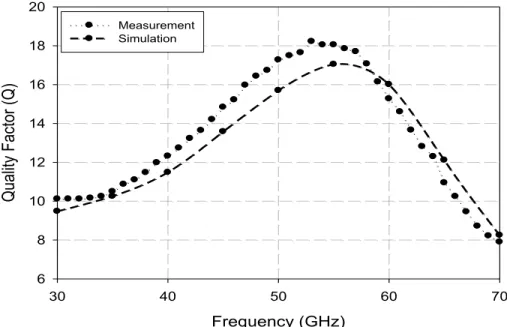
Fig. 4.12 Simulation and measured Q-factor for PGS-CPW ... 68
Fig. 5.1 Measurement pad equivalent circuit ……….. 72
Fig. 5.2 Impedance matching ………... 72
Fig. 5.3 Low-pass prototype for the filter synthesis ………… 73
Fig. 5.4 EM simulator simplified model of dielectric………... 75
Fig. 5.5 Simulated S-parameter to compare real dielectric
and simplified dielectric ………. 76 Fig. 5.6 Metal layers structure in CMOS process and layout
designed of 60GHz OLR-BPF ……… 77 Fig. 5.7 Model of the 60GHz BPF with two-pole second
order open loop resonators with patterned ground
illustrated using 3D EMS ……….. 79 Fig. 5.8 Proposed BPF employing folded open loop
resonators ……... 79 Fig. 5.9 Equivalent model exhibiting electric coupling for a
0⁰ feed structure ………... 80 Fig. 5.10 Comparison of S21 for different tapping positions
in OLR-BPF with folded structure……… 81 Fig. 5.11 Folding structure of the BPF and simulated S-
parameter ... 82 Fig. 5.12 Comparison of current distribution of BPF with
and without folded structure ………. 83 Fig. 5.13 Effect of folded structure in open loop resonator ….. 83 Fig. 5.14 Effect of patterned ground shield on attenuation
characteristics of microstrip line at 60GHz………… 84 Fig. 5.15 Patterned ground shield BPF ……… 85 Fig. 5.16 Comparison of insertion losses of the OLR-BPF
with and without patterned ground shield…………. 86 Fig. 5.17 BPF with CSRR as ground shield ……… 86 Fig. 5.18 Layout structure of the BPF with SRR ………... 87 Fig. 5.19 Simulation results on the effect of placing SRRs
either on M5 or M2 of CMOS layer …. ………... 88
Fig. 5.20 BPF construction with (a) 5-SRRs and (b) 2-SRRs .. 89
Fig. 5.21 5-quadrilateral SRRs on folded BPF ………... 90 Fig. 5.22 5-conventional SRRs on BPF ……… 90 Fig. 5.23 Chip photo of the proposed two-poles BPF (Chip
size = 650 x 810μm
2including bonding pads) ….….. 91 Fig. 5.24 Chip photo of the proposed four-poles BPF (Chip
size = 905 x 810μm
2including bonding pads) ….….. 91 Fig. 5.25 Comparison of S-parameters of the proposed two-
poles BPF ………... 92
Fig. 5.26 Comparison of S-parameters of the proposed four-
poles BPF ………... 93
Fig. 5.27 BPF with CSRR as ground shield ……… 93 Fig. 5.28 Results of BPF with CSRR as ground shield ………. 94 Fig. 5.29 Chip photo of the BPF ………. 95 Fig. 5.30 Simulated and measured results of the proposed
BPF ……….. 96
Fig. 5.31 Chip photo of 5-SRRs and 2-SRRs ……… 96 Fig. 5.32 Simulated S-parameter of BPF with 5-SRRs ……… 97 Fig. 5.33 Measured result of BPF with 5-SRRs and 2-SRRs .. 98 Fig. 5.34 Chip photo of 5-quadrilateral SRRs on folded BPF . 98 Fig. 5.35 Measured results of 5-quadrilateral SRRs on folded
BPF ……….. 99
Fig. 5.36 Chip photo of 5-conventional SRRs on folded BPF .. 100 Fig. 5.37 Results of 5-conventional SRRs on folded BPF ……. 100 Fig. 5.38 Coupling coefficients for different structure of
BPFs and effect of placing SRRs either on M2 or
M5……… 103
List of Tables
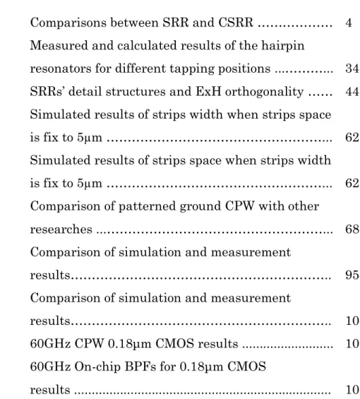
Table 1.1 Comparisons between SRR and CSRR ……… 4 Table 3.1 Measured and calculated results of the hairpin
resonators for different tapping positions ...………... 34 Table 3.2 SRRs’ detail structures and ExH orthogonality …… 44 Table 4.1 Simulated results of strips width when strips space
is fix to 5µm ………... 62 Table 4.2 Simulated results of strips space when strips width
is fix to 5µm ………... 62 Table 4.3 Comparison of patterned ground CPW with other
researches ...………... 68 Table 5.1 Comparison of simulation and measurement
results……….. 95
Table 5.2 Comparison of simulation and measurement
results……….. 102
Table 6.1 60GHz CPW 0.18μm CMOS results ... 106 Table 6.2 60GHz On-chip BPFs for 0.18μm CMOS
results ... 107
Chapter 1 Introduction
1.1 Background
Millimeter-wave (mm-wave) frequency band is the most promising technology in broadband wireless communication. Since the released of rules governing the usage of frequency between 57 and 66GHz by Federal Communications Commissions (FCC) in 2001, large bandwidth with high allowable transmit power and high data rates becomes popular [1].
Traditionally, semiconductor technologies based on III-V compound e.g.
Indium Phosphide (InP) and Gallium Arsenide (GaAs) are applied. Due to rapid progress and high demand, Complementary Metal Oxide Silicon (CMOS) technology is used in the mm-wave applications because of its low cost and high level of integration thus enabling easy Systems-On-Chip (SoC) solution [2][3].
Low resistivity of the semiconducting silicon substrate causes serious
signal loss of the passive devices. As the frequency increase, attenuation
becomes larger and mm-wave system implementation becomes very
challenging for IC designers since designs would require very large path loss and require higher chip-size. Thus, transmission line with low loss and higher performance is needed to solve this problem. Currently, there are several issues regarding on-chip transmission lines such as [4];
requirement of low loss lines with best performance as the frequency increases;
accurate circuit simulations that can predict the attenuation, phase constant and characteristic impedance correctly;
minimization of the used of metal densities and distances limitation in designing CMOS structure.
Difficulty in realizing the 50Ω transmission lines makes the ground coplanar waveguide (G-CPW) is not an effective solution to reduce the losses [5]. This is because, by inserting the metal shields below the signal line lowering the line inductance leads to increase of eddy current and increase the losses of respective design.
Several attempts have been made to reduce the size of the chip
including implementation of inductive stub loading, aggressive meandering,
slow wave structure and multilayer design techniques [6]. Among all those
mention, slow wave structure provides higher quality factor (Q) and lower
attenuation. Slow wave concept was introduced by Hasegawa in early 70’s
[7]. Slow wave structure extensively used in non-monolithic, multi-dielectric
substrates in order to achieve frequency selective behavior in microwave
passive circuit. In mm-wave applications, transmission line is the basic
element with great importance especially in designing passive devices and
interconnection with active devices. Although microstrip line is far the most
popular microwave transmission line for designing integrated circuits (IC),
due to unintended circuit response and dispersion, coplanar waveguide (CPW) transmission line is preferable in this research which has great advantages compare to microstrip line. With slow wave technique, the chip size could be reduces as well as decreasing the dielectric loss of the design.
Slow wave technique is applied through the design of patterned ground shield placed at the lowest metal (M1) of the CMOS layers.
Recently, many bandpass filters (BPFs) for 60GHz mm-waveband utilizing CMOS process have been proposed by researchers [8]-[10]. However, most of the designed BPFs have various disadvantages, e.g. high insertion loss, inadequate selectivity response, large chip size, or too wide band pass.
These disadvantages make them difficult to be employed in the 60GHz wireless communications standard. For example, the lumped component BPF showed excellent selectivity response and compact size, however, the 6.9dB insertion loss is too high to be employed in real implementation [8]. In ref. [9], dual-mode loop resonator BPF presented good selectivity response, nevertheless, the 4.9 dB insertion loss was still relatively high, and moreover, large chip size and special input position restricted its application.
The folded microstrip line BPF successfully employed at 60GHz with
insertion loss of 2.7dB, however it is difficult to be utilized in the 60GHz
waveband wireless internet standard because of its more than 30GHz
bandwidth [10]. Implementing split ring resonator (SRR) in filters’ design is
becoming great interest nowadays. SRR is one of the main structures used in
metamaterial design and it is widely applied in filters, directional couplers
and other passive components design which has the unique properties of
both permittivity and permeability [11][12]. It consists of small resonant
particles with a high quality factor at microwave frequencies. In contrast to
SRR is the complimentary SRR (CSRR) which has a connected metallic
ground plane extends over all the structure. The different between SRR and
CSRR are summarized in Table 1.1.
Table 1.1
Comparison between SRR and CSRR
SRR CSRR
Structure
Descriptions/
Details
Planar structures, and wires can easily substituted by metallic strips
Contrast to SRR
Etched in the back substrate side, below the slots, to achieve high magnetic coupling between line and rings at resonance.
Etched on the ground plane at regions where the electromagnetic field is significant
Presence of the rings leads to an effective negative-valued
permeability in a narrow band above resonance, where signal propagation is inhibited.
Significantly very small in size than
conventional resonator structures (generally less than one-tenth of a wavelength enabling the design of very compact filters
Metal Slot Metal
Slot
1.2 Motivations
In current wireless communication system, market demand on the high data rate services is becoming increasing. Thus, in the next few years, wireless LAN and wireless PAN data rates should be within the range of 1-10Gbps.
60GHz frequency band could offer larger bandwidth leads to higher data rate (>1Gbps). Besides, it also provides, high transmit power and greater range. Small form factors of antenna (short wavelengths) with lower interference and longer range (high directivity) could be realized in 60GHz frequency band. Fig. 1.1 shows the current trends in wireless communication data rate and technologies [13].
Silicon technology is the dominant material for semiconductors design market compare to GaAs process which remained very small. It comprises about 95% of the semiconductor industry compare to 5% of the arsenide market [14]. Silicon technology has several advantages over GaAs. It is readily available with good thermal conductivity (> 2.75 times) compared to arsenide. Although GaAs technology offers higher performance circuits design, silicon process is cheaper in terms of cost of manufacturing with lower power consumption compare to GaAs technology.
Transmission line is the basic element in higher frequency application.
It is used in the design of passive devices and interconnects for active device.
Lossy silicon problem could be solved by applying the slow wave propagation technique.
The biggest challenges for IC designers in designing filters in CMOS process are higher insertion loss and lower selectivity. Major issues need to be considered when designing the filters include loss induced by substrate.
This loss exists due to electrical coupling that degrade the Q-factor of the
resonators. Thus, proper coupling model between adjacent resonators to
reduce the coupling value need to be considered. Besides, thin silicon oxide layer between signal layer and ground plane and thick metal layer result regime where edge and fringe capacitances are significant. Between top metal slab and bottom edge, current distribution and voltage potential (E-H distributions) is not the same. On the other issues, the multi-layer structure of CMOS die makes the determination of the electromagnetic field distribution of a transmission line or a filter design structure very difficult to be calculated.
Fig. 1.1 Current trend in the wireless communication data rate and technologies [13]
Recently, 60GHz BPF has been designed in the CMOS technology, but
has several limitations as mentioned earlier. A low loss BPF with good
selectivity and desired bandwidth is important in reducing the burden of
power amplifier in 60GHz system. Fig. 1.2 shows the 60GHz wireless
transceiver [15]. For the sake of obtaining enough power gain in this mm-
waveband, numerous designers have to use complex multi-stage amplifier or even use costly special production process to design a power amplifier (PA).
At the same time, the consumer markets force the manufacture to produce
electric and communications products with low power and low cost. The
method regarding to improve the power added efficiency (PAE) of mm-band
PA becomes the focal point for RFIC engineers in recent years. In the
receiver part, BPF used to reject out-of-band interference and improve the
receiver sensitivity. Therefore, research on decreasing the insertion loss of
the BPF is of great importance. It is desired to have filters which could be
integrated with the transceiver to reduce overall cost and form factor of the
radio system. One of the biggest challenges for IC designers from integrating
RF filters on CMOS is the lossy silicon substrate. Silicon substrate induces
higher resistive loss which occurs due to deterioration of quality factors of
resonators as the result of electrical coupling which leads to higher insertion
loss of filters.
Fig. 1.2 Block diagram for 60GHz wireless transceiver [15]
On the other side, the design and analysis of passive RF filter is a challenging task since the thick metal layers and thin multi-dielectric material on CMOS [15]. These make the current distribution and the voltage potential between the top surface and bottom surface is not identical.
Besides, thick metal would result fringing coupling based on the sidewalls of
metal traces that make the design method inaccurate. Thus, more
significant approach must be taken into consideration to accurately design
the filter.
1.3 Research objectives
The objectives of this thesis are to develop slow wave passive devices for mm-wave application and can be summarized as follows:
to design, simulate and fabricate low-loss coplanar waveguide (CPW) transmission line by applying slow wave propagation technique to exhibit higher Q-factor;
to design, simulate and fabricate bandpass filter (BPF) with patterned ground shield and split ring resonators (SRRs) as ground layer to achieve low insertion loss, small bandwidth;
to design, simulate and fabricate patterned ground shield BPF with multiple SRRs, classical and quadrilateral SRRs achieve low insertion loss, small bandwidth and compact size.
1.4 Thesis outline
This thesis include five (5) chapters altogether. The chapters are constructed and arranged accordingly to the development of the slow wave structure for the 60GHz technology with major design focusing on the mm-wave transmission line, coplanar waveguide (CPW) and bandpass filters (BPFs) design.
Chapter 1 is the Introduction of the thesis. It covers background of the
study, motivations, design objectives and thesis outline.
Chapter 2 entitled, Design of CMOS 60GHz mm-wave transmission line, discuss on mm-wave transmission line. Among other type of transmission lines, for example, microstrip and stripline, coplanar waveguide (CPW) is selected in this design due to several advantages mentioned in this chapter. This chapter includes subtopics of CMOS, slow wave concept, mechanisms of loss, introduction of metal shields and patterned ground in the passive components design and recent researches in 60GHz mm-wave applications.
Chapter 3 is Design of 60GHz bandpass filters (BPFs) with split rings and methodology. 60GHz Bandpass filter (BPF) and split ring resonator (SRR) explained hypothetical of 60GHz BPF with SRR as one of famous metamaterial structures. BPF plays very important role in mm-wave applications. In this chapter, filter design methods, characteristics and tradeoffs are explained. SRR is presented in this chapter as one of the important characteristic in designing the filter. Beside, design methodology is also included in this chapter. It includes flow-chart of design procedure.
Chapter 4 is Development of low-loss 60GHz coplanar waveguide transmission line with patterned ground shield. In this chapter, CPW is design with patterned ground shield design as the ground layer of the CMOS structure. Metal strips’ space and and widths are first determined by using calculation and simulation method before designing the patterned structure to be applied in the CPW design. Both measurement and simulation results are presented in this chapter
Chapter 5 entitled, Development of 60GHz bandpass filters (BPFs) on
patterned ground shield and split ring resonator (SRR). In this chapter, the
author introduces the concept of SRR towards the design of the BPF in order
to achieve better performance of filter. Different considerations are well
explained in this chapter referring to the best way in choosing the structure of SRR to be used for higher frequency applications. Basically, BPF is constructed with open loop resonators and folded structure with patterned ground shield. Different structures and placements of SRR are designed below the BPF structure either as ground shield or increasing the numbers of SRR in order to examine the effect of the SRR toward enhancing the performance of current BPF designed. This chapter also includes measurement and simulations results of BPFs consist of two poles and fourth poles BPFs, 2 and 5-quadrilateral SRRs on BPFs, 5-quadrilateral SRRs on folded BPF, 5-conventional SRRs on BPF and BPF with CSRR as ground shield.
Last but not least, is Chapter 6 which covers Conclusion and future
works. This chapter concludes this thesis with two main designs, the CPW
and BPFs which operates at mm-wave frequency band. It is recommended
that the structure of the BPF should be decreased to quarter wavelength size
to solve the problem of area and also increase the performance of the filter
with different structure of ground. Thus, the lossy silicon substrate is not a
major issue in designing passive components for higher frequency system.
Chapter 2
Design of CMOS 60GHz mm-wave transmission line
2.1 Introduction
In mm-wave technology, due to the increasing demand for comprehensive
applications, the transmission capacity of the wireless internet is required
for further improvement. Since the well-known, 802.11 series wireless
communications standards apparently cannot satisfy today’s high
requirements, e.g. transmitting data at 10Mbps for a single task, the
unlicensed 60GHz waveband wireless network standard is preferable which
can offer more than 1Gbps internet capacity. This is quite suitable for local
communication applications which involve high transmitting density. The
applications of 60GHz mm-waveband bring tremendous challenges to the
design of the transmission system. Fig. 2.1 shows the available spectrum in
the mm-wave applications for certain country around the world [1].
Fig. 2.1 Available spectrum in 60GHz band for indoor wireless communication around the world [1]
60GHz wireless communication offers abundance of the bandwidth which is unmatched in any of the lower frequency bands. Besides, unlicensed and largely harmonized across most regulatory regions makes this range of frequency bands to be the most promising technology in the wireless communication in contrast with the meager spectrum available in the lower frequency band [1]. On the other hand, due to recent advances in Complementary metal-oxide-semiconductor (CMOS) makes this frequency band feasible to build inexpensive and low power transceiver components.
2.2 Complementary metal–oxide–semiconductor (CMOS) CMOS is particularly attractive for 60GHz band applications because of the low cost, easy for large-scale manufacture and its potential of integration with back-end circuits, enabling easy systems-on-chip (SoC) solution.
2.3 CMOS mm-wave transmission lines
Transmission lines play important role for mm-wave applications. The
improvement of transmission lines is important as it is the most basic
configuration in a system for realizing other devices such as filters, baluns,
power dividers/combiners and couplers [2]. There are several types of mm- wave transmission lines; common types include microstrip line, coplanar waveguide (CPW) and grounded coplanar waveguide (G-CPW) as shown in Fig. 2.2. Due to unintended circuit responses and larger dispersion, G-CPW is preferable in this research.
Fig. 2.2 Common microwave transmission line structures
2.3.1 Coplanar waveguide transmission line
Coplanar waveguide (CPW) is a transmission line geometry that includes a central current-carrying trace on top of a dielectric substrate, with side ground extending beyond a symmetric gap to either side of a trace. G-CPW has an additional ground below the substrate; while ungrounded CPW has side grounds coplanar to the signal trace provide the only return path. CPW is generally defined by center strip width (w), gap (g), substrate height (h), and substrate dielectric material (t).
Several advantages of CPW over microstrip line are listed as follow;
lower loss tangent than microstrip line because signals coupled mostly through air;
characteristic impedance, Z
ocan be controlled by varying the trace width, the space-to-ground, and the dielectric or material;
low dielectric losses between surface mounted components and in
underlying ground plane (ungrounded CPW);
signal is carried on an exposed surface trace where a surface mount component can be attached;
provides good inherent crosstalk immunity for two layer boards because it is less sensitive to the presence or absence of a backside of board ground plane;
in CPW design, via-holes are not necessary and fragile semiconductors don’t need to be excessively thin, with limitation of individual component sizes, thus reducing the processing costs [2].
One of the advantages of CPW is that it allows a wider signal and ground path to be used because the distance between signal path and ground is not set by the dielectric thickness. Increasing the gap will lowering the ground capacitance, allowing a wider signal path to be used. But, the ground conductors of a CPW do not shield the signal inductor from the underlying substrate. If the gap size is bigger than dielectric thickness, there is a significant loss of energy in the substrate. Wide signal paths and large gaps suffer from attenuation and low Q-factor due to losses on silicon MMIC.
More electromagnetic field would leak into the substrate due to the wider gap. The best way to solve this problem is by introducing floating metal shield below the metallization plane.
Fig. 2.3 shows a ground-signal-ground cross section of CPW where
metal strips (i.e metal not connected to any circuit nodes) are placed below
the CPW as floating shield. Since the shield is a good conductor, there is no
electric field tangential to the strips. For a component of the electric field
from the CPW to enter the substrate vertically, the shield must be subject to
a net electric flux from the CPW (i.e net electric field summed over the area
of the shield) [3]. However, this is not the case because there is no net charge
on the CPW. Thus, the voltage on the shield is at 0V with respect to the CPW, and the floating strips can act as an effective electric shield between CPW line and the substrate. Moreover, unlike an explicitly grounded substrate shield that is susceptible to circuit parasitic (such as parasitic inductance), the floating shield remains close to 0V regardless of the selection of signal and ground conductor widths. Similarly, a floating shield stays at 0V when applied to a pair of coplanar differential transmission lines as indicate in differential diagram in Fig. 2.3.
Fig. 2.3 CPW with floating metal shield and differential [3]
2.3.2 Silicon substrate in mm-wave applications and slow wave concept
One of the biggest challenges that hinder designers from integrating RF passive devices on CMOS is the lossy silicon substrate. High resistive loss induced in the silicon substrate due to electrical coupling deteriorates the quality factor of resonators implemented on CMOS which leads to higher insertion loss of filters based on these resonators. Conventionally, GaAs is used in passive device design process. The construction of metals in the GaAs substrate is shown in Fig. 2.4(a). In this design, the off-chip ground is directly serves as a common voltage reference and return current path for
y
Total net charge of CPW= 0 Shield equidistant to CPW 0 Shield made of metal E =0
Ez
shield
below shield 0 0 E V
- - - + + - - - + +
+
Ground Signal Ground
“Floating
metal shield”
Silicon Substrate
E
zE
yon-chip components. Later, the design of slow wave mm-wave CMOS is implemented in the silicon substrate with thin metal layer is inserted between the substrate and top metal as shown in Fig. 2.4(b). This layer consist of arrangement of thin strips normally between 0.3 µm to 1 µm for each strip. The size of each strip is designed to be as small as possible because of holes or slots are added to the design to prevent stress-induced intermetal dielectric cracking. It is a formation of voids in interconnections of metals caused by induced stressed from the mismatch in thermal expansion coefficients (TCE) between metal line and silicon substrate. The on-chip ground is connected using bondwires with the off-circuit chip ground.
The ground on silicon MMIC has some voltage swing unlike the GaAs
technologies.
(a) (b)
Fig. 2.4 Metal interconnect schemes in production of III-V GaAs technology and slow wave design implemented in Si substrate [3]
Semiconducting silicon substrates with 1-20 Ω.cm resistivity used in
manufacturing mixed-signal RF ICs and the conductive substrate is a well-
known caused of signal loss in passive devices. Patterned ground shield has been introduced to minimize the RF energy coupled into the substrate. The shield is placed between the metal and silicon substrate to reduce the electric field leaking into the silicon substrate [3]. In practical, it is difficult to implement an on-chip reference that does not suffer from voltage variations (due to parasitic from circuit and package interconnections).
Besides that, at higher frequency, IC designer faced different losses in terms of conductor/ohmic loss, dielectric loss and radiation loss.
Conductor loss occurs because of similarity between rectangular waveguides with finite conductivity of metallic walls. This type of loss can be minimized by designing the feed network length per wavelength as short as possible. It is also referred as ohmic loss when the size of the design area is smaller when higher frequency is applied. Dielectric loss exists because of loss tangent of dielectric medium and it can be reduced by using substrate with a low dielectric loss. Radiation loss is exist due to presence of gaps along the side walls and possible leakage through the gaps. To minimize this type of loss, the number of discontinuities such as bends and T-junctions should be made as small as possible. In mm-wave applications, one of the solutions to reduce the loss on the silicon substrate is by designing pattern ground structure between the silicon substrate and metallization plane to produce the effect of slow wave propagation.
Slow wave technique reduces the size of the circuit in terms of the
length of the transmission lines. Transmission lines with periodic shunt and
series decrease the phase velocity, thereby increasing the effective electric
length of the line. This can be characterized by relationship between
characteristic impedance, 𝑍
𝑐and phase velocity, 𝑉
𝑝, given as;
Where L and C are the inductance and capacitance per unit length of the line respectively. If the capacitance or inductance per unit length in a physically smooth transmission line is increased by changing its physical layout configuration, it automatically decreases its inductance or capacitance per unit length. However, if capacitances in shunt and inductance in series are added at periodic intervals along the length and the spacing between the added capacitors is small enough compared to the wavelength, it can be anticipated that the line will appear to be electrically smooth with the effective characteristic impedance and the phase velocity given as ;
and
The phase velocity could be lowered and its effective characteristic impedance may be changed due to the effect of periodic loading. If 𝑉
𝑝,𝑙𝑜𝑎𝑑𝑒𝑑is the phase velocity of the periodically loaded line then the physical length, l of the loaded transmission line is given by;
.
p loaded, ol V
Where ∅ is the electric length of the loaded transmission line
c
Z L
C 1 V
p LC
, c loaded
L L
Z C C
,
1
p loaded
V L L C C
(2.1) (2.2)
(2.4) (2.3)
(2.6)
Lowering the phase velocity means that an effectively long electric length can be realized with a shorter physical length. According to this theory, shortening and miniaturizing circuits can be designed by slow wave structure of periodically loaded capacitance or inductance.
2.3.3 Metal shield and floating strips
In mm-wave transmission line, dielectric losses due to the silicon substrate
can be minimized by insertion of a metal shield between the silicon substrate
and metallization plan as shown in Fig. 2.5 and Fig. 2.6.
Fig. 2.5 Front view of CPW without metal shield/ground plane
With insertion of metal shield, electromagnetic field penetrating to the SiO
2substrate will be decreased and produced eddy current. Eddy currents (also called Foucault currents) would cause the changing of the original magnetic field and lowering the inductance per unit length and
Si substrate
Si substrate
characteristic impedance, small value of dielectric effective permittivity, and poor quality factors [4][5].
Floating strips were introduced by Hasegawa in 1977 by using GaAs substrates but suffer from high insertion loss [6]. The spacing between the strips should be kept to a minimum distance to maximize the boost effect as well as shielding the structure from the lossy, silicon substrate. This is due to the decrease in unit cell capacitance, or rather the decrease in the ratio of length with an artificial dielectric strip to the length without the strip. For a CPW transmission line, the capacitance is measured between the signal potential and ground potential, where capacitance will increase as the distance decreases, while for inductance is measured between the signal path and return current path, where this property is increased if the length is increased. Fig. 2.7 shows the floating strips place as ground in CPW construction [6].
Fig. 2.7 Floating strips [6]
The asymmetrical coaxial waveguide concept is illustrated in Fig. 2.8
where an increase of area, A1 enclosed with farther side ground metals
results larger inductance, while distance between the signal line and ground
potential, d
ois decreased which allows larger capacitance to be achieved.
Fig. 2.8 Asymmetrical coaxial waveguide concept [7]
Wider gap between the signal and ground can resulted a relatively high inductance and floating shield minimizing the substrate loss. If the shield strips are short (i.e. order of microns in the direction of the current flow), the current induced onto the shield strips by signal current is negligible. Therefore, the line inductance is not affected by the shield.
However, the shield strips add parasitic capacitance between the signal and the ground paths resulting the line inductance and capacitance of the original CPW to increase simultaneously by the addition of the floating shield strips [3].It has been reported that, narrow ground planes can be used to implement high frequency electrical performances of the S-CPW transmission line, but for conventional CPW transmission lines the ground planes width should be fairly large to minimize the ground inductance [8].
Compared to unshielded CPW, the line capacitance of the floating shielded CPW is increased due to the addition of metal shielding strips
.
1L B A t
o o
C A
d
: Magnetic flux density : Dielectric permittivity B
Electric field
Bottom of pad metal
Magnetic flux B
Top of lower shield
A
1A
od
oBUT, line inductance is
virtually unaffected because
current induced in the shield
is minimized as the length of
each strip is small in the
direction of signal
propagation.
Shielding structure can slow down signal propagation and thus lowering the wavelength that is adjustable in the physical design of a circuit.
The minimal spacing and length allowed by the technology is 1.6μm. It is shown that narrow and finely spaced (<2 μm) metal strips is required to maximize the performance of the transmission line [3]. Minimal strip length (SL) suppresses induced current flow thus minimizing ohmic loss and reduction of line inductance and maximizing the reactive energy storage per unit length. These will also minimizing the eddy currents. Besides, using the smallest shield strip spacing allowable minimizing the exposure of the overlying CPW to the conductive subsrate and to boost the shield effect from the lossy silicon substrate [6].
Referring to Maxwell simulations, when power is important for considerations, providing the metal layers do not substantially lower the characteristic impedance of the line because the electric field for the grounded coplanar structure is already spread between the coplanar ground lines and bottom ground line. Thus, adding the additional metal layers does not perturb this field substantially where the per unit capacitance for the GCPW structure is 0.063 pF/mm while the per unit capacitance for the S- GCPW structure is 0.067 pF/mm. [9].
2.3.4 Patterned ground shield
Patterned ground shield could increase the Q-factor to almost 50% of the
inductor. Fig. 2.9 shows the patterned ground shield with slots orthogonal to
the spiral designed to increase the resistance of the image current. The slots
act as an open circuit to cut off the path of the induced loop current. It
should be as narrow as possible so that the vertical electric field cannot leak
through the patterned ground shield into the substrate below it. The ground
strips act as the termination for the electric field. The shield should be strapped with the top layer metal to provide a low impedance path to ground.
The main reason is to prevent negative mutual coupling and minimizing the impedance to ground. As the magnetic field passes through the patterned ground shield, its intensity is weakened due to the skin effect [10]. This directly causes a decrease in the inductance since the magnetic flux is lessened in the space occupied by the ground shield layer. To avoid this attenuation, the shield must be significantly thinner than the skin depth at the frequency of interest. For example, the skin depth of aluminum at 2GHz is approximately 2m, which is only three times the typical metal-one thickness. This implies that using a typical metal one layer for the shield may result in reduction of the magnetic field intensity and, hence, the inductance.
Fig. 2.9 Patterned ground shield [10]
2.3.5 Recent researches on mm-wave transmission lines
Numbers of researches have been conducted with the implementation of
slow wave propagation technique to improve the performance of passive
devices. A 0.13μm CMOS is designed with grounded metal strips with two metal layers arranged in zigzags to prevent the penetration of electric field thus reducing the loss of the signal line [11]. With the used of two metal would eliminate the parasitic coupled slotline mode without requiring additional air bridges and increasing the dielectric permittivity where the signal is concentrated around the signal path. Fig. 2.10 shows the cross section of this design.
Fig. 2.10 (a) Simplified structure and (b) cross-section of the proposed S- MSL [11]
In 90μm technology, Q-factor of 7 and attenuation of 2.7dB/mm and
phase constant of 4.352 rad/mm are achieved as shown in Fig. 2.11 [12]. The
ground metal is designed at both sides (CPW) with extended metal fingers
orthogonal to the direction of current flow and connected at distance from
the signal conductor. Ground conductor is connected to a slotted ground
underneath the signal line to prevent electric field and minimizing return current.
Guided microstrip line (GMSL) with sides and bottom walls is also designed in 65nm CMOS process as shown in Fig. 2.12 [13]. This design structure solves the problems of dummy metals. Recently, dummy metals are placed in design to fulfill the density rules, but parasitic capacitance would exist degrading the performance of transmission line. This design achieved Q-factor of 14, attenuation of 2.4 rad/mm. The differences between all researches mentioned are summarized in Fig. 2.13.
Fig. 2.11 Micrograph of the fabricated structure [12]
Fig. 2.12 The structure of the guided microstrip line [13]
Fig. 2.13 Comparison between researches in ref. [11]-[13]
2.4 Conclusion
In this chapter, the slow wave concept that could solve the problem of lossy
silicon substrate applied in the mm-wave CMOS transmission line is
explained. This technique is introduced since 1977 by a Japanese researcher
is applied in many IC designs process nowadays. Metal shield consisting of
metal strips with slots is placed as the ground layer to improve the
performance of the mm-wave transmission lines thus reducing the design
area. Slow wave technique is the cheapest (save the cost of manufacturing)
compare to other techniques such as implementing stub loading, aggressive
meandering and multilayer substrate in higher frequency design.
Chapter 3
Design of 60GHz Bandpass Filters (BPFs) with Split Rings and Methodology
3.1 Introduction
Radio frequency (RF) filters play very important role in mm-wave
applications. RF filter is used to pass the desired signal to broadcast, keeps
the signals un-interfered with other signals and vice versa. Since amplifier
consumes the most power, good amplifier efficiency is needed in realizing the
60GHz system. Although different application have been used (e.g. by using
complex multi-stage amplifier or costly special production process) the
method regarding to improve the PAE of the PA becomes the main point for
RFIC designers. But, a good PA is difficult to be realized in higher frequency
band. Thus, the best choice for IC designers is by designing a low insertion loss and high selectivity BPF that could reduce the burden of the amplifiers.
Fig. 3.1 shows the 60GHz transceiver [1].
Fig. 3.1 Block diagram for 60GHz transceiver
3.2 Filter design methods
In designing filter, there are two different methods that can be applied,
image parameter method (IPM) and insertion loss method (ILM). IPM
consists of a cascade of simpler two-port filter sections to provide desired
cutoff frequency and attenuation characteristics. This type of filter design
does not allow the specification of a frequency response over the completed
operating range. Although the design process is simple, IPM often must be
iterated many times to achieve desired result. Nevertheless, this method is
important for simple filters which produce good relationship between infinite
periodic structures and practical filter design. In ILM, network synthesis
techniques are used to design filter with a completely specified frequency response. ILM process starts with filter specifications include the cutoff frequency, stop-band attenuation, pass-band insertion loss, pass-band behavior and etc. Then, low pass prototype circuit with R=1Ω (source and load resistances) and 𝜔
𝑐= 1
𝑟𝑎𝑑𝑠is designed. In this step, filter tables are used to determined filters parameters for any types of filters. These steps are illustrated in Fig. 3.2.
Fig. 3.2 ILM filter design process
Prototype filter is derived from Fig. 3.3 via L and C values for a second order low pass filter.
Fig. 3.3 Second order low pass filter Filter
specifications
Low pass prototype
design
scaling and
conversion Implementation
V
SL
C R 1
Z
in+
-
(3.3) Input impedance is calculated using Eqn. (3.1) where,
𝑍
𝑖𝑛= 𝑗𝜔𝐿 + 𝑅(1 − 𝑗𝜔𝑅𝐶) 1 + 𝜔
2𝑅
2𝐶
2The reflection coefficient at the input port is,
Γ = 𝑍
𝑖𝑛− 1 𝑍
𝑖𝑛+ 1
In ILM, a filter response is defined by its insertion loss, or the power loss ratio, 𝑃
𝐿𝑅given as,
𝑃
𝐿𝑅= 𝑃𝑜𝑤𝑒𝑟 𝑎𝑣𝑎𝑖𝑙𝑎𝑏𝑙𝑒 𝑓𝑟𝑜𝑚 𝑡ℎ𝑒 𝑠𝑜𝑢𝑟𝑐𝑒
𝑃𝑜𝑤𝑒𝑟 𝑑𝑒𝑙𝑖𝑣𝑒𝑟𝑒𝑑 𝑡𝑜 𝑙𝑜𝑎𝑑 = 𝑃
𝐼𝑛𝑐𝑃
𝑙𝑜𝑎𝑑= 𝑃
𝐿𝑅= 1 1 − |Γ(𝜔)|
2Then, integrating Eqn. (3.3) to Eqn. (3.2), the new 𝑃
𝐿𝑅is,
𝑃
𝐿𝑅= [1 − 𝑍
𝑖𝑛− 1
𝑍
𝑖𝑛+ 1 . 𝑍
𝑖𝑛∗− 1
𝑍
𝑖𝑛∗+ 1 ]
−1= |𝑍
𝑖𝑛+ 1|
22(𝑍
𝑖𝑛+ 𝑍
𝑖𝑛∗)
Maximally flat filter response normally called the binomial or Butterworth response that provides the flattest possible passband response for a given order. Thus, by assuming k = 1, then
𝑃
𝐿𝑅= 1 + ( 𝜔
𝜔
𝑐) = 1 + 𝜔
4𝑓𝑜𝑟 𝑁 = 1, 𝜔
𝑐= 1
Equating Eqn. (3.4) and Eqn. (3.5), it shows that 𝑅 = 1 since 𝑃
𝐿𝑅= 1 𝑓𝑜𝑟 𝜔 = 0, and 𝐿 = 𝐶 = √2.
(3.1)
(3.5) (3.2)
(3.4)
ILM offers a high degree of control over the passband and stopband amplitude and phase characteristics, with a systematic way to synthesize a desired response compare to IPM. This criterion is important, since a minimum insertion loss is needed in designing a filter. In all cases, this method allows filter performance to be improved in a straightforward manner, at the expense of a higher order filter.
3.3 Bandpass filter characteristics
Conventional RF filter design practice uses a series of coupled resonant sections in order to increase selectivity of the filter and broaden the desired band. For example, the ring resonator filter has bandpass characteristics. If a ring is coupled to input and output transmission lines, the signal will pass through with certain losses at the resonant frequencies of the ring and will be rejected at frequencies outside the resonant frequencies.
Various band-pass filtering characteristics can be designed by
cascading several ring resonators in series. Ring resonators can support two
degenerate modes if both modes are excited to form the base for a compact
dual mode filter. Fig. 3.4 shows that ring resonators can be designed via
slotline, microstrip and coplanar waveguide.
Fig. 3.4 Ring resonators designed
By combining the properties of low-pass and high-pass into a single filter, a band-pass filter can be designed as illustrated in Fig. 3.5 and Fig.
3.6.
Fig. 3.5 System level block diagram of a bandpass filter
Fig. 3.6 Bandpass filter circuit
Ring resonators
design
Microstrip
Slotline Coplanar
waveguide
V
inR
1C
1R
2C
2V
outI
Low pass filter High pass filter Signal
Input
Signal Output Blocks frequencies
that are too high
Blocks frequencies
that are too low
Filters with cross-coupled structure are used to achieve high selectivity characteristics with transmission zeros that can improve the skirt rejection of the microstrip filters [3]. Fig. 3.8 shows filter configuration, where the resonators are divided into sections of 𝑙
1and 𝑙
2. The total length of the resonator is half of the guided wavelength at fundamental resonance frequency.
Fig. 3.8 Filter using two hairpin resonators with asymmetric tapping feed lines [3]
By letting 𝑆
21= 0 , transmission zeros can be found corresponding to the tapping positions (given a small value of 𝐶
𝑠1), given as,
𝑓
1=
4𝑙 𝑛𝑐1√𝜀𝑒𝑓𝑓
𝑎𝑛𝑑 𝑓
2=
4𝑙 𝑛𝑐2√𝜀𝑒𝑓𝑓
, n = 1,3,5, …
Where 𝑓
1and 𝑓
2are the frequencies of two transmission zeros based on tapping positions, 𝜀
𝑒𝑓𝑓is the effective dielectric constant, n is the mode number, c is the speed of light in free space and 𝑙
1and 𝑙
2is the length of the resonators. Maximum rejection will occur at transmission zeros, with 𝑆
21= 0.
Measured result for different tapping positions for filter in Fig. 3.8 is shown in Fig. 3.8 with fundamental frequency of 2GHz, fabricated on a RT/Duroid 6010.2 substrate with thickness h = 25mil , relative dielectric
(3.6)
constant 𝜀
𝑟= 10.2 . Table 3.1 summarized both measured and simulated results for different tapping positions.
Fig. 3.8 Measured results for different tapping positions with coupling gap 𝑠
1= 0.35𝑚𝑚 [3]
Table 3.1
Measured and calculated results of the hairpin resonators for different tapping positions [3]
Measurements Calculations 𝑙
1= 𝑙
2= 𝑙 2 = 14.43𝑚𝑚 ⁄ No passband at
2GHz
𝑓
1= 𝑓
2= 2𝐺𝐻𝑧
𝑙
1= 12.69𝑚𝑚, 𝑙
2= 16.16𝑚𝑚
𝑓
1= 1.8𝐺𝐻𝑧 𝑓
1= 1.79𝐺𝐻𝑧 𝑓
2= 2.25𝐺𝐻𝑧 𝑓
2= 2.27𝐺𝐻𝑧 𝑙
1= 11.24𝑚𝑚,
𝑙
2= 17.61𝑚𝑚
𝑓
1= 1.68𝐺𝐻𝑧 𝑓
1= 1.64𝐺𝐻𝑧
𝑓
2= 2.48𝐺𝐻𝑧 𝑓
2= 2.57𝐺𝐻𝑧
A high selectivity filter would result minimum insertion loss. In microwave filter, the cross coupling between non-adjacent resonators creates transmission zeros that can improve the skirt rejection of the microstrip filters. Without proper coupling, the cavities would act as one single resonator. As shown in Fig. 3.9, two hairpin resonators are designed with asymmetric feed lines tapping the resonators. This type of filter is more compact with 45-degree chamfered bends and the coupling gap g = 5um between the two open ends of the ring.
Fig. 3.9 Layout of the filter using two open-loop ring resonators with asymmetric tapping feed lines [3]
Chamfered bend is designed to a curve in microstrip line as shown in
Fig. 3.10. In RF and microwave circuit, designers need an automated way to
specify the ratio of the chamfering in order to minimize losses. The distance
between the 90° corner and chamfer is critical.
Fig. 3.10 Microstrip bend
For optimum chamfer, the ratio of the width of the chamfered region, b to the width of the microstrip line is w, is approximately,
and capacitance , C and inductance value, L of,
By considering a transfer function
Where Ω, is the frequency variable that is normalized to the passband cutoff frequency of a low-pass prototype filter, ε is a ripple constant related to a given return loss L
Rin decibels by
b 0.5 w
180
20.001 3.393 0.62 7.6 3.8
90
r rw w
C h
h h
0.947
0.177( / )
0.44 180 1 1.062 90
L h e
w h
2
21 2 2
![Fig. 1.1 Current trend in the wireless communication data rate and technologies [13]](https://thumb-ap.123doks.com/thumbv2/123deta/9920184.1920539/22.918.229.684.444.757/fig-current-trend-wireless-communication-data-rate-technologies.webp)
![Fig. 2.1 Available spectrum in 60GHz band for indoor wireless communication around the world [1]](https://thumb-ap.123doks.com/thumbv2/123deta/9920184.1920539/29.918.200.721.185.359/fig-available-spectrum-ghz-indoor-wireless-communication-world.webp)
![Fig. 2.4 Metal interconnect schemes in production of III-V GaAs technology and slow wave design implemented in Si substrate [3]](https://thumb-ap.123doks.com/thumbv2/123deta/9920184.1920539/33.918.168.748.517.909/metal-interconnect-schemes-production-technology-design-implemented-substrate.webp)