Precautions when handling our products
Cautions regarding this document
DSGD. CHKD.
KS TN YS
KS TN YS APPD. DOCUMENT No.
SYMB. APPD. CHKD. DSGD. ( 1/14 )
DATASHEET
~ Revision 01-2 ~
1) For the export of products which are controlled items subject to foreign and domestic export laws and regulations, you must obtain approval and/or follow the formalities of such laws and regulations. 2) Products must not be used for military and/or antisocial purposes such as terrorism, and shall not be supplied to any party intending to use the products for such purposes.
3) Unless provided for otherwise, the products have been designed and manufactured for application in equipment and devices which are sold to end users in the market, including audio-visual (AV) equipment, electrical home appliances, office machines, information and communication equipment, and amusement equipment. The products are not intended for use in, and must not be used for, any application for nuclear equipment, driving equipment for aerospace or any other unauthorized use.
With the exception of the abovementioned prohibited applications, please contact an Alps sales representative and/or evaluate the total system regarding applicability for applications involving high levels of safety and liability such as medical equipment, burglar alarm equipment, disaster
prevention equipment and undersea equipment. Please also incorporate fail-safe design, protection and redundant circuitry, malfunction protection, and/or fire protection into the complete system to ensure safety and reliability of the total system.
4) Before using products which were not specifically designed for use in automotive applications, please contact an Alps sales representative.
1) The specifications herein are an overview of the specifications. Obtain official specifications before use.
2) The external appearance, functions and other specifications herein may be discontinued without prior notice.
DATASHEET
HGDVST021A
ALPS P/N: HGDVST021A
2015-07-19
DATEK.SEJIMO
SBD GD-589Y.SUDA
2015-07-19
2017-06-28T.NAKAMURA
2016-09-142015-07-19
ALPS ELECTRIC CO.,LTD.
1 2
( 2/14 )
List of Contents
1
Product Description
製品説明3
1.1 Overview
概要3
1.2 Target Applications
ターゲットアプリケーション3
2
Functional Description
機能説明4
2.1 Pin Configuration
ピン配置4
2.2 Pin Description
ピン機能4
2.3 Block Diagram
ブロックダイアグラム4
3
Specifications
仕様5
3.1 Application Circuit
アプリケーション回路5
3.2 Absolute Maximum Ratings
絶対最大定格5
3.3 Recommended Operating Conditions
推奨動作条件6
3.4 Basic Characteristics
基本特性6
3.5 Magnetic Characteristics
磁気特性7
4
Package Information
パッケージ情報8
4.1 Package Outline
外形図 84.2 Footprint
フットプリント8
4.3 Distance between Chip and Package
チップ/パーッケージ間距離9
4.4 Package Marking
捺印9
5
Packing Specifications
梱包仕様10
5.1 Packing Information
梱包情報10
6
Precautions When Handling Magnetic Sensor
製品お取り扱い時の注意11
6.1 Storage Environment
保管環境11
6.2 Long-term Storage
長期保管11
6.3 ESD
静電気ESD11
Appendix
A1 List of Figures
図のリスト12
A2 List of Tables
表のリスト12
A3 Revision History
改定履歴13
DATASHEET
ALPS P/N: HGDVST021A
SBD GD-589
( 3/14 )
1
Product Description
製品説明1.1 Overview
概要ALPS Product No. HGDVST021A Characteristic Magnetic Switch
Package type SOT-23
Supply Voltage 3.0 to 30 V
Supply Current 1mA
Interface Open Drain Output
Temperature -40 to 140 deg.C
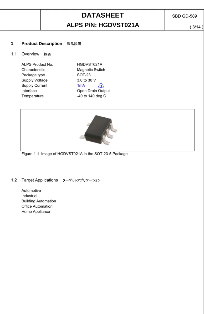
Figure 1-1 Image of HGDVST021A in the SOT-23-5 Package
1.2 Target Applications
ターゲットアプリケーション Automotive Industrial Building Automation Office Automation Home ApplianceSBD GD-589
DATASHEET
ALPS P/N: HGDVST021A
2( 4/14)
2
Functional Description
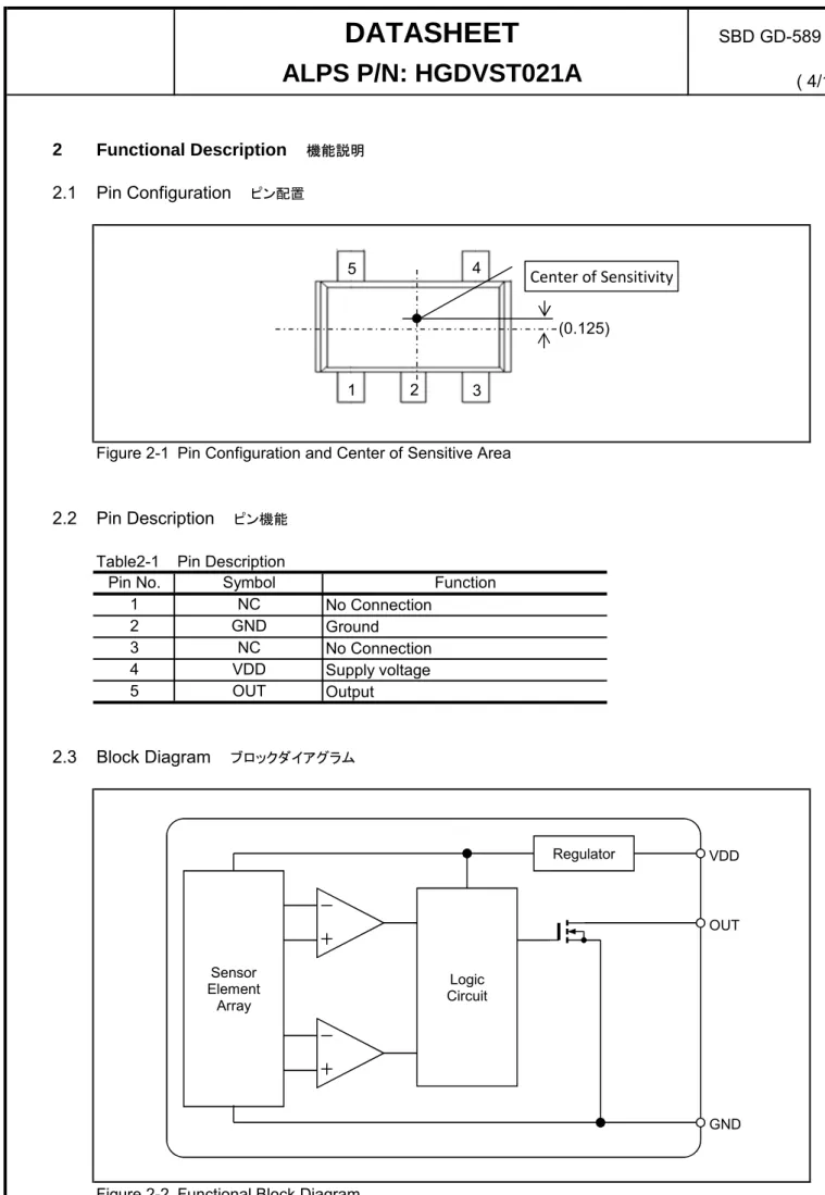
機能説明2.1 Pin Configuration
ピン配置Figure 2-1 Pin Configuration and Center of Sensitive Area
2.2 Pin Description
ピン機能 Table2-1 Pin DescriptionNo Connection Ground No Connection Supply voltage Output
2.3 Block Diagram
ブロックダイアグラムFigure 2-2 Functional Block Diagram
SBD GD-589
3 2 Pin No.DATASHEET
ALPS P/N: HGDVST021A
1 Symbol Function NC GND NC VDD 5 OUT 4 1 2 3 4 5 (0.125)Center of Sensitivity
Sensor Element Array Logic Circuit Regulator VDD OUT GND( 5/14 )
3
Specifications
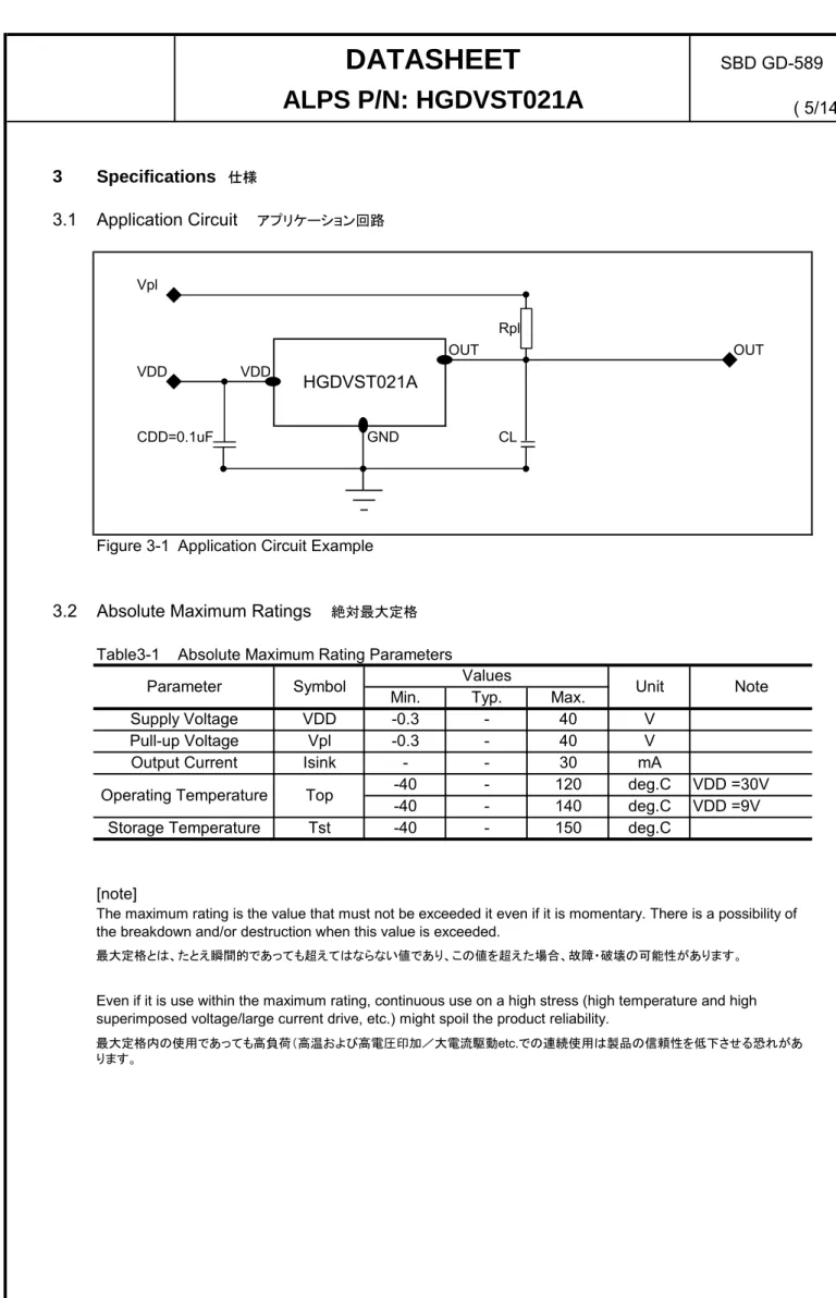
仕様3.1 Application Circuit
アプリケーション回路 Vpl Rpl OUT OUT VDD VDD CDD=0.1uF GND CLFigure 3-1 Application Circuit Example
3.2 Absolute Maximum Ratings
絶対最大定格 Table3-1 Absolute Maximum Rating Parameters[note]
deg.C VDD =9V
The maximum rating is the value that must not be exceeded it even if it is momentary. There is a possibility of the breakdown and/or destruction when this value is exceeded.
最大定格とは、たとえ瞬間的であっても超えてはならない値であり、この値を超えた場合、故障・破壊の可能性があります。
Even if it is use within the maximum rating, continuous use on a high stress (high temperature and high superimposed voltage/large current drive, etc.) might spoil the product reliability.
Storage Temperature Tst Top
最大定格内の使用であっても高負荷(高温および高電圧印加/大電流駆動etc.での連続使用は製品の信頼性を低下させる恐れがあ ります。
Output Current Isink - - 30 mA
-40 - 120 deg.C VDD =30V
Supply Voltage VDD -0.3 - 40
Pull-up Voltage Vpl -0.3 - 40
HGDVST021A
Parameter Symbol Values Unit Note
Min. Typ. Max.
deg.C -40 - 150 -40 - 140 V V
SBD GD-589
DATASHEET
ALPS P/N: HGDVST021A
Operating Temperature( 6/14 )
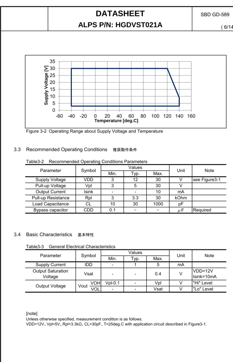
Figure 3-2 Operating Range about Supply Voltage and Temperature
3.3 Recommended Operating Conditions
推奨動作条件 Table3-2 Recommended Operating Conditions Parameters3.4 Basic Characteristics
基本特性Table3-3 General Electrical Characteristics
VOH VOL
[note]
Unless otherwise specified, measurement condition is as follows.
VDD=12V、Vpl=5V、Rpl=3.3kΩ、CL=30pF、T=25deg.C with application circuit described in Figure3-1. V "Hi" Level - - Vsat V "Lo" Level
Output Voltage Vout Vpl-0.1 - Vpl
mA Output Saturation
Voltage Vsat - - 0.4 V
VDD=12V Isink=10mA
Supply Current IDD - 1 5
Parameter Symbol Values Unit Note
Min. Typ. Max.
Output Current Isink - - 10
pF
Bypass capacitor CDD 0.1 - - μF Required
Load Capacitance CL 10 30 1000
SBD GD-589
DATASHEET
Parameter Symbol Values Unit Note
Min. Typ. Max.
see Figure3-1 Pull-up Voltage Vpl 3 5 30 V
ALPS P/N: HGDVST021A
VDD 3 12 30 V Supply Voltage mAPull-up Resistance Rpl 3 3.3 30 kOhm
0
5
10
15
20
25
30
35
-60 -40 -20
0
20
40
60
80 100 120 140 160
Supply Volta g e [V] Temperature [deg.C]( 7/14 )
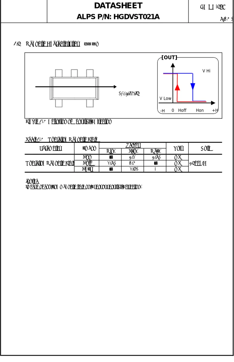
3.5 Magnetic Characteristics
磁気特性Figure 3-4 Definition of Sensitivity Direction
Table3-4 Operating Magnetic Field
[note]
In case of applying magnetic field only sensor sensitivity direction.
(2.7) -(0.6) 1.4 Hon Hoff Hhys -(0.7)
DATASHEET
ALPS P/N: HGDVST021A
mT mTSBD GD-589
Parameter Symbol Values Unit Note
Min. Typ. Max.
2.0 mT
Operating Magnetic Field 25deg.C
-
-+
Sensitivity
V Hi V Low 0 Hoff Hon +H[OUT]
-H( 8/14 )
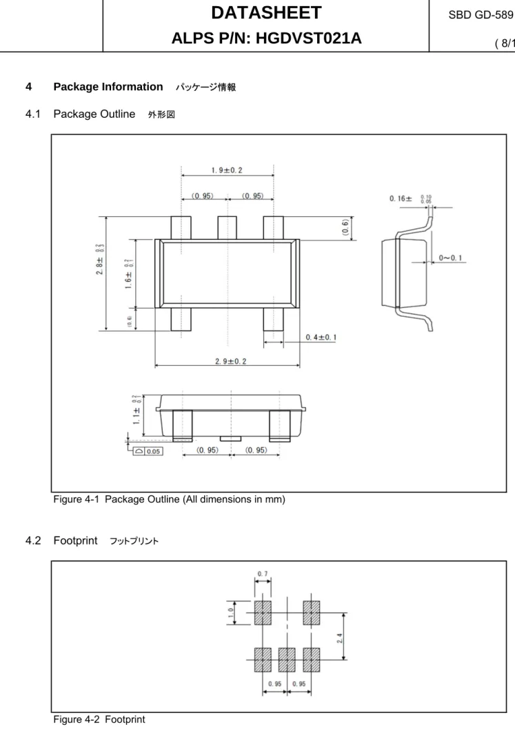
4
Package Information
パッケージ情報4.1 Package Outline
外形図Figure 4-1 Package Outline (All dimensions in mm)
4.2 Footprint
フットプリントFigure 4-2 Footprint
DATASHEET
ALPS P/N: HGDVST021A
( 9/14 )
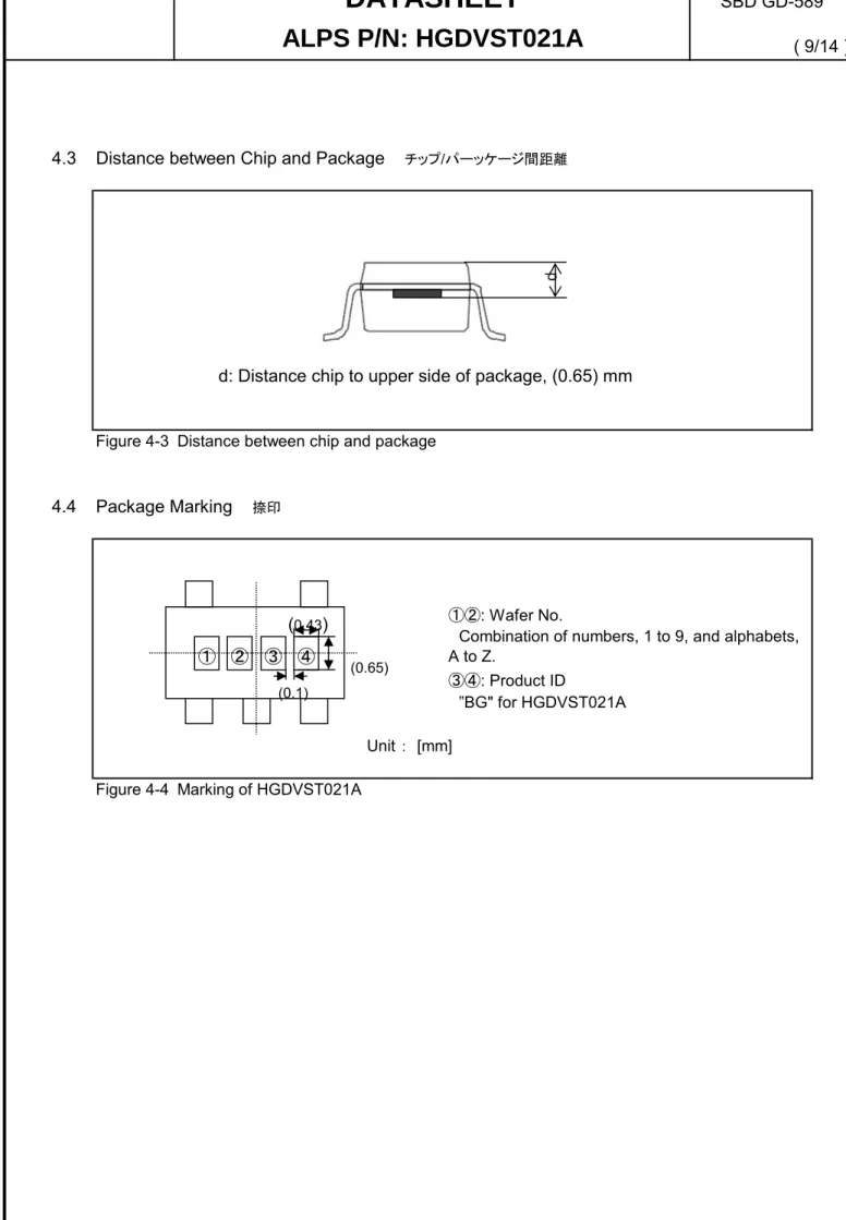
4.3 Distance between Chip and Package
チップ/パーッケージ間距離d: Distance chip to upper side of package, (0.65) mm
Figure 4-3 Distance between chip and package
4.4 Package Marking
捺印①②: Wafer No.
③④: Product ID
”BG" for HGDVST021A Unit : [mm]
Figure 4-4 Marking of HGDVST021A
SBD GD-589
DATASHEET
ALPS P/N: HGDVST021A
Combination of numbers, 1 to 9, and alphabets, A to Z.
④
① ② ③
(0.65)(
0.43)
(0.1)( 10/14 )
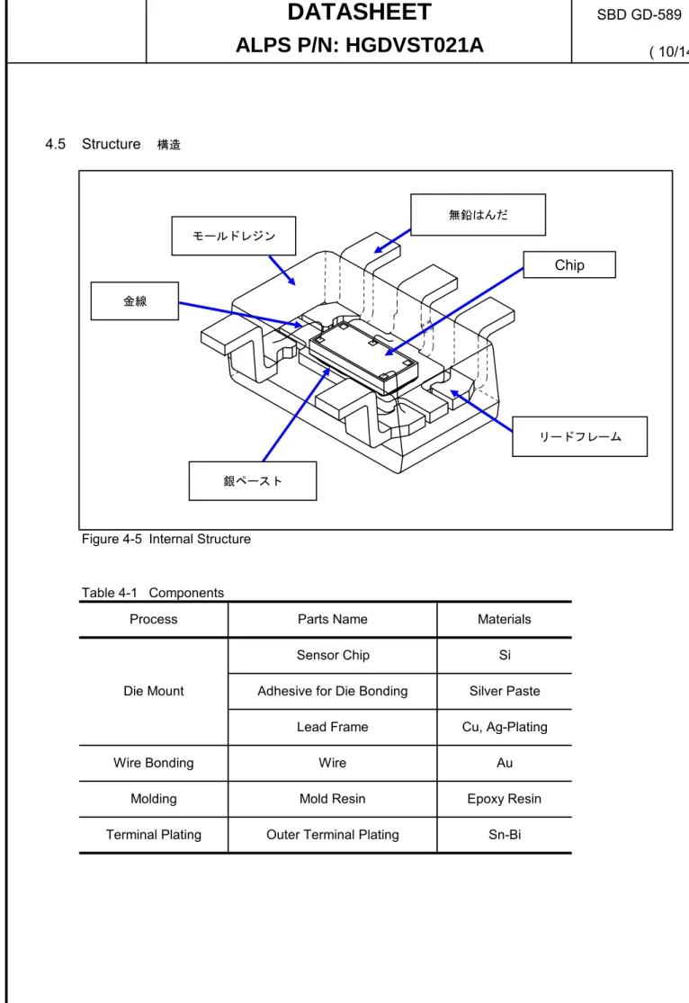
4.5 Structure
構造Figure 4-5 Internal Structure
Table 4-1 Components
SBD GD-589
Process Parts Name Materials
Die Mount
DATASHEET
ALPS P/N: HGDVST021A
Sensor Chip Si
Adhesive for Die Bonding Silver Paste Lead Frame Cu, Ag-Plating
Terminal Plating Outer Terminal Plating Sn-Bi
Wire Bonding Wire Au
Molding Mold Resin Epoxy Resin
Chip
金線 リードフレーム 無鉛はんだ 銀ペースト モールドレジン( 11/14 )
5
Packing Specifications
梱包仕様5.1 Packing Information
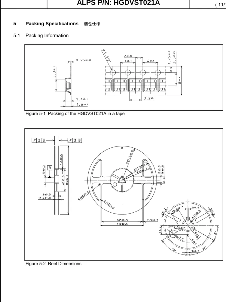
Figure 5-1 Packing of the HGDVST021A in a tape
Figure 5-2 Reel Dimensions
SBD GD-589
DATASHEET
( 12/14 )
6
Precautions When Handling Magnetic Sensor
製品お取り扱い時の注意6.1 Storage Environment
保管環境6.2 Long-term Storage
長期保管6.3 ESD
静電気ESDLong-term storage may result in poor lead solder ability and degraded electrical performance even under proper conditions. For those part that stored more than 1 year, solder ability should be checked before use. For storage longer than 1 year, it is recommended to store in nitrogen atmosphere. Oxygen in atmosphere oxidant leads of products and lead solder ability get worse. 適切な保管環境でも長期に保管した場合は、リ-ド端子の半田付け性が悪くなったり、電気特性が不良になる場合が ありますので、長期保管した場合は、半田付け性や電気特性をご確認の上、ご使用下さい。保管が長期(1年以上)に 及ぶ場合は、窒素雰囲気中での保管をお勧めします。大気中で保管されますと、大気中の酸素により素子のリ-ド部 分が酸化され、リ-ド端子の半田付け性が悪くなります。
Every products has built in ESD protect circuit, however it may break if over ESD applied to this circuit. Please take measure for ESD when handle the products. Conducted container is recommended for product conveyance and packing instead of plastic container. Please connect ground line and use non high voltage leakage, when using soldering iron or external measurement circuit. 全ての端子に接続されたICについて静電気保護回路を内蔵していますが、その能力を超える静電気が加わった場合 には破壊されることがありますので、製品を取り扱う場合には充分な静電気対策を実施してください。包装・運搬容器 はプラスチック製を極力避け、導電容器をご使用ください。また製品のハンドリングについても充分に考慮してください。 (リストストラップの使用等)はんだごてや測定回路などは高電圧リークのないものを、必ずアースを取ってご使用くださ い
DATASHEET
ALPS P/N: HGDVST021A
SBD GD-589
Products should be stored at an appropriate temperature and humidity (Recommended storage condition). Keep products away from chlorine and corrosive gas. There is a thing that influences product features when keeping it in an improper environment.
適切な温度・湿度環境(推奨保管条件)で保管していただけるようお願いします。また、塩素や腐食性のあるガスも避け るようお願いします。不適切な環境で保管した場合は、製品特性に影響する事があります。