Japan Advanced Institute of Science and Technology
Title その場TEM観察による架橋されたグラフェンナノリボン
電気伝導の構造依存性
Author(s) LIU, CHUNMENG Citation
Issue Date 2020‑09
Type Thesis or Dissertation Text version ETD
URL http://hdl.handle.net/10119/17013 Rights
Description Supervisor:大島 義文, 先端科学技術研究科, 博士
Doctoral Dissertation
Structure-Dependent Electrical Conductance of Suspended Graphene Nanoribbon by In-situ Transmission Electron Microscopy Observation
Liu Chunmeng
Supervisor: Professor Yoshifumi Oshima
Graduate School of Advanced Science and Technology Japan Advanced Institute of Science and Technology
[Materials Science]
September 2020
I
Structure-Dependent Electrical Conductance of Suspended Graphene Nanoribbon by In-situ Transmission Electron Microscopy Observation
Liu Chunmeng s1720432
In this thesis, the structure-dependent electronic properties of suspended graphene nanoribbons (GNRs) are investigated by in situ transmission electron microscopy (TEM) observation to obtain structural information and simultaneous current-voltage (I-V) curve measurements.
The suspended GNR devices are fabricated with the width from ca. 100 to 800 nm. After careful cleaning by current annealing, the suspended ribbon sculpt by convergent electron beam followed by a high bias annealing. During the thinning process, the measured I-V curves indicate that the electrical conductivity of ribbon change from metallic to semiconducting behavior, with the reduction of GNR width. When the width become very narrow (usually < 4 nm), the energy gap start to be opened. A transport gap of 300 and 700 meV is estimated for 1.5 nm wide AGNR and ZGNR, respectively. Most of important, the I-V curves for the zigzag edge GNRs (ZGNRs) are obviously different from those for the armchair edge GNRs (AGNRs) and mixture of both zigzag and armchair edges GNRs (MGNRs) as follows. (1) The ZGNRs showed a sharp increase at the threshold voltage in differential conductance- voltage curves. (2) The band gaps measured for ZGNRs were smaller than the band gaps calculated using the GW approximation. (3) The threshold voltage increased with the GNR length. These features support the previously simulated current-driven magnetic-insulator and nonmagnetic-metal nonequilibrium phase transitions by the application of a bias voltage.
In addition, we also carefully observe the restructure of monolayer and few layer GNRs under different applied bias voltage. When a stable 1.0 V bias voltage is applied on monolayer GNR, it only affect the edge structure; the rough and curve edge restructure into straight and smooth edge, without changing the width of ribbon. However, when the bias voltage is increased, it not only affect edge structure, but also width and layer number of GNR. Under a high bias voltage, the thickness and width of ribbon shrinks sharply with the edge restructure at the same time. Moreover, we found that the conductance improve by structure recrystallization during reconstruction process, even with the decrease of ribbon width.
In conclusion, our ability to fabricate ultra-narrow GNRs with controlled width, layer number and edge structure opens a door systematic investigation the structure dependent electrical property of GNR.
The unique I-V characterization of narrow and short ZGNR represents the potential for further nanosized switching devices.
Keywords: structure-dependent electronic properties, suspended graphene nanoribbons, in-situ TEM observation, nonequilibrium phase transitions, restructure
Abstract ... I
Chapter 1 Background ... 1
Introduction ... 1
1.1 Graphene and graphene nanoribbon ... 2
1.1.1 The basic introduction of graphene ... 2
1.1.2 Graphene nanoribbon and its electrical property ... 4
1.1.3 The preparation of graphene nanoribbon ... 8
1.2 Basis of transmission electron microscopy and characterization ... 9
1.3 The previous investigation of GNR: A brief review ... 12
1.4 Purpose and method of present research ... 16
1.5 Conclusion ... 17
Reference ... 19
Chapter 2 Experimental setup and sample preparation ... 24
Introduction ... 24
2.1 Experimental setup ... 25
2.2 The design of in-situ TEM holder... 26
2.3 The design of custom TEM chip... 28
2.4 The fabrication of GNR device ... 29
2.4.1 List of equipment used for fabrication ... 29
2.4.2 The overall process of fabrication ... 34
2.4.3 Electrodes fabrication ... 36
2.4.4 Fabrication of nano-gaps on the electrode ... 40
2.6 Conclusion ... 49
References ... 50
Chapter 3 Graphene cleaning methods ... 52
Introduction ... 52
3.1 Consideration on cleaning of graphene ... 53
3.2 Dry-cleaning with adsorbents ... 54
3.3 Two-step annealing in gas environment ... 58
3.4 Thermal annealing in vacuum ... 61
3.5 In-situ current induced-annealing ... 65
3.5.1 The damage of GNR under electron beam before cleaning ... 65
3.5.2 Current annealing process of GNR ... 66
3.5.3 The mechanism of in-situ current annealing... 69
3.5.4 Finite element method simulation of suspended GNR devices ... 74
3.6 Conclusion ... 80
References ... 81
Chapter 4 Nano-sculpting and in-situ electrical measurement of graphene nanoribbons ... 84
Introduction ... 84
4.1 Rough nano-sculpting of the GNR device ... 85
4.2 Precise thinning process and I-V measurement of narrow GNR ... 88
4.2.1 The thinning process of GNR by applying a high bias voltage ... 88
4.2.2 In-situ I-V measurements during thinning process ... 90
4.3 Resistance measurement of GNR with different widths ... 97
4.4 Structure-dependent electronic properties of ultra-narrow AGNR and ZGNR ... 98
4.4.1 The electrical conductance properties of AGNRs ... 98
4.4.2 I-V curves for ultra-narrow ZGNRs ... 100
4.4.3 Interpretation of I-V curves for ZGNRs ... 103
4.5 Conclusion ... 107
References ... 108
Chapter 5 Restructure of graphene nanoribbon under bias voltage ... 113
Introduction ... 113
5.1 Edge recrystallization of monolayer GNR ... 114
5.2 Improvement of conductance for monolayer GNR during reconstruction .. 120
5.3 Layer sublimation and reorganization of few layer GNR ... 123
5.4 Conclusion ... 126
References ... 128
Chapter 6 Summary ... 130
Appendix A ... 133
Acknowledgements ... 136
List of Publications ... 138
Presentation ... 139
1
Chapter 1 Background
Introduction
The first chapter will introduce the mainly investigated topic of this thesis-graphene nanoribbon, and explains how to use in-situ transmission microscopy to study this material.
In Chapter 1.1, we introduce what is graphene and graphene nanoribbon, and how to make the ribbon. In Chapter 1.2, we show the construction and working principle of a transmission electron microscopy and explain how it works in this experiment. In Chapter 1.3, we give a brief overview of recent theoretical and experimental progress about the investigation of graphene nanoribbon. In Chapter 1.4, we show the mainly method and purpose in this thesis.
2
1.1 Graphene and graphene nanoribbon
1.1.1 The basic introduction of graphene
Graphene- a two dimensional (2D) allotrope of carbon- has attracted widely attention due to the unique properties and applications. It consists of one atom thick carbon film, which arranges in a honeycomb structure made out of hexagons, shown in Figure 1.1(a). Although it’s the basic of other carbon materials: fullerenes, carbon tubes and graphite, it was discovered long time later after its invention. The reason is that, the limit of equipment to search for one-atom-thick flakes and no one believe graphene can stable exist in the free state.
Figure 1.1 Models of graphene and graphene nanoribbon. (a) Graphene is 2D building materials for graphene nanoribbon by cutting the main crystallographic axis. The yellow part indicate the obtained ribbon. (b) Graphene nanoribbon along zigzag (blue color) or armchair (red color) directions.
3
Until 2004 year, Geim and Novoselov1 successfully peel off single graphitic plane with the tape from graphite and place it on a silicon /silicon dioxide (Si/SiO2) substrate, which allow its observation with an ordinary optical microscopy.2-4 This discovery not only gained the Noble Prize in physics in 2010, but also opens up a new research topic of 2D materials in material physics. The fascination with graphene has been growing very rapidly and the physics of graphene is becoming one of the most interesting and fast-moving topics in condensed-matter physics. Many of the interesting physical phenomena appearing in graphene are governed by a very peculiar band structure, which the other 2D materials do not have. Its unique band structure equivalent to a relativistic massless particle gives rise to unusual electronic properties quite different from those of conventional systems. With a simple tight-binding calculation,5 we see that there are two special points in the Brillouin Zone (BZ), called K and K’, where the energy dispersion is linear with the momentum, with zero gap between the conduction and valence bands. The position where the conduction band and valence band touch at is so-called Dirac point.6-8 It corresponds to a topologically singular point around which an electronic states acquires a geometrical phase factor called Berry’s phase. It is responsible for the peculiar behavior in the transport properties, such as the minimum conductivity,9 the dynamical conductivity,10 and the localization effect.5, 11 The high
4
speed massless, fermionic quasiparticles in graphene which travel at the Fermi velocity of vF = 106 m/s (300 times slower than light), lead to the chiral tunneling and Klein paradox and the anomalous integer quantum Hall effect.5
1.1.2 Graphene nanoribbon and its electrical property
However, being a zero band gap material, perfect graphene is not suitable for semiconductor electronic devices. For example, when we plan to fabricate a Field Effect Transistor (FET) with graphene, it is impossible to turn off the electronic current flowing in the channel as a switch. This should be a fundamental requirement of a logic gate. Therefore a band gap should be induce into graphene, and keep its intrinsic unique characteristics, such as high electron mobility, thermal conductivity, mechanical strength and low noise.
One of the possible method is making graphene into nanometer-scale graphene nanoribbon (GNR) with either armchair or zigzag edges,12, 13 as shown in Figure 1.1(b).
Both the first principle calculation and experiments have shown that a band gap could be opened in nano-scaled armchair-GNRs (AGNRs) or zigzag-GNRs (ZGNRs). The origin of the band gap is dependent on the edge structure, i.e., zigzag or armchair.
Although the mechanisms of this bandgap is different between AGNR and ZGNR, both the scales of band gap as the inverse of the ribbon width. The band gap of AGNR has
5
been reported to be caused by quantum confinement, while that of ZGNR is caused by spin polarization around the zigzag edges.14
Since the electrical conduction property of GNR is strongly dependent on the structure (especially edge state), it is important to investigate the relationship between them. It has been theoretically pointed out that when the width of ribbon width is 10 nm or less, the contribution of the edge state to the electric conduction becomes extremely important. Graphene nanoribbons correspond to a structure in which carbon nanotubes (CNT) are cut open along their axes. This edge structure can be defined by a chiral vector corresponding to the circumference of the carbon nanotube, and the vector perpendicular thereto corresponds to the edge of the ribbon. Assuming the basic lattice vectors with angle of 60°are as shown in Figure 1.2 (a), the chiral vector is defined as follows.
𝑪𝒉 = 𝑛𝒂 + 𝑚𝒃, 1-1 and (𝑛, 𝑚) is called the chiral index. The edges of both sides of the single-walled carbon nanotube are connected, which means they have a periodic boundary condition with a period of the chiral vector. On the other hand, graphene nanoribbons are terminated by edges on both sides, and have a boundary condition having the width of the chiral vector.
Figure 1.2 (b) shows the extended Brillouin zone of graphene, the wave vector
6
corresponding to the chiral vector period of single-walled carbon nanotubes 𝜥𝟏, and 𝜥𝟐which vector is perpendicular to 𝜥𝟏. As mentioned above, the electronic state of graphene has no energy gap only at K and K '. From this, if the group of line segments parallel to the wave vector just intersects with K and K', such single-walled carbon nanotubes have no energy gap and show metallic properties. Otherwise, it has a semiconductor-like property.
Figure 1.2 (a) Unit cell of graphene and (b) Extended Brillouin zone
The condition for showing metallic properties should be as below, 𝑲 ∙ 𝑲𝟏
|𝑲𝟏| = 𝑛|𝑲𝟏| or 𝑲′ ∙ 𝑲𝟏
|𝑲𝟏|= 𝑛|𝑲𝟏| (n; integer) 1-2 Let us express the vector in the reciprocal lattice space in Figure 1.2 (b) by the basic vector a1, a2 in the real space. The basic vector in reciprocal lattice as shown:
𝒃𝟏= 2
3𝑎2(2𝒂𝟏− 𝒂𝟐), 𝒃𝟐= 2
3𝑎2(−𝒂𝟏+ 2𝒂𝟐) 1-3 Wave vector 𝜥𝟏 corresponding to the chiral vector period can be expressed as:
7
𝜥𝟏 =|𝑪1
𝒉|𝟐𝑪𝒉 = 1
𝑎2(𝑛2+𝑛𝑚+𝑚2)(𝑛𝒂𝟏+ 𝑚𝒂𝟐) 1-4 |𝜥𝟏| = 1
𝑎√𝑛2+𝑛𝑚+𝑚2 1-5 K and K ' can express as:
𝑲 = 1
3(𝟐𝒃𝟏+ 𝒃𝟐) = 2
3𝑎2𝒂𝟏 1-6 𝑲′ =1
3(𝒃𝟏+ 𝟐𝒃𝟐) = 2
3𝑎2𝒂𝟐 1-7 From above calculation, equation 1-2 can be expressed as:
𝑲 ∙ 𝑲𝟏
|𝑲𝟏|2 =2𝑛+𝑚
3 1-8 𝑲′∙ 𝑲𝟏
|𝑲𝟏|2= 𝑛+2𝑚
3 1-9 Therefore, from equation 1-8 and 1-9, when 2𝑛 + 𝑚 or 𝑛 + 2𝑚 becomes an integer multiple of 3,cutting line intersects K point or K' point.From the above, it can be found that the electrical property of CNT becomes a metal when 𝑛 − 𝑚 becomes a multiple of 3.
This result also can apply to GNR. As we said above, the edge structure of GNR is divided into two typical types, which are called zigzag edges (blue line in Figure 1.1(b)) and armchair edges (red line in Figure 1.1(b)). For a zigzag edge, its chiral exponent (𝑛, 𝑚 ) has the relationship of 𝑛 = 𝑚 . In other words, when “𝑛 − 𝑚 becomes a multiple of 3” is satisfied, it is expected that the zigzag edge GNR has metallic properties. In the case of an armchair edge, the chiral index (𝑛, 𝑚) has the relationship of 𝑛 = 0 or 𝑚 = 0 or 𝑛 = −𝑚. When the condition “𝑛 − 𝑚 becomes a multiple of
8
3” is satisfied or not satisfied, it is expected that the metal or semiconductor properties will be obtained depending on the chiral index. On the other hand, it has been reported that, when the spin is taken into consideration, the result is different from the above result.
1.1.3 The preparation of graphene nanoribbon
In experiments, there are many different methods used to fabricate GNRs. Among them, it can be mainly separated into two kinds, bottom-up and top-down. Although bottom-up method can fabricate GNR with long length and atomically sharp edges by chemically synthetization from basic organic molecules, the synthesized ribbon have a contact with metal substrate, which influence the intrinsic property of GNR. In another top-down method, the ribbon could be fabricated from a large graphene flake. With this method, the undesired parts can be removed by many methods, such as: atomic force microscope (AFM) direct lithography,15 scanning tunnel microscope (STM) lithography,16 plasma etching (usually oxygen and hydrogen),13, 17 and catalytic etching (usually metal partials).18 Recently, another new top-down method has been achieved, with the development of in situ transmission electron microscopy (TEM) / scanning transmission electron microscopy (STEM) technology. In this method, electron beam in
9
TEM directly used to sculpt graphene and pattern it into desired ribbons. Since this method was also used in this thesis, we will explained it more detail and deeply in the following chapters.
1.2 Basis of transmission electron microscopy and characterization
Transmission electron microscope is a modern comprehensive large-scale analytical instrument, which is widely used in the research and development of modern science and technology. Just as the name implies, the so-called electron microscope is a microscope that uses an electron beam as a light source. The electron beam can bend under the effect of an external magnetic field or electric field, forming a refraction phenomenon similar to that when visible light passes through glass. Then this physical phenomenon was used to create the "lens" of the electron beam, and developed the electron microscope. The special feature for TEM is that the image is formed by the electron beam which go through the sample. That is the difference from the scanning electron microscope (SEM). Since the wavelength of the electron wave is much shorter than the wavelength of visible light (the wavelength of an electron wave of 100 kV is 0.0037 nm, and the wavelength of violet light is 400 nm), according to optical theory, we can expect that the resolving power of an electron microscope should be much better than that of an optical microscope. In fact, the resolving power of modern electron
10
microscopes has reached 0.1 nm.
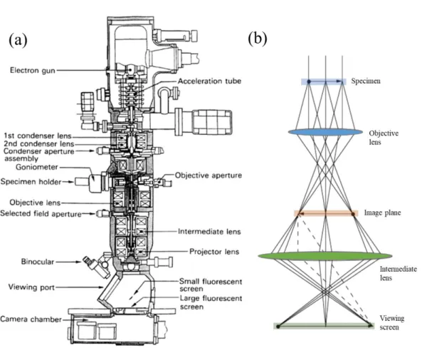
Now we will briefly introduce the components and working principle of TEM. The schematic of a TEM is shown in Figure 1.3 (a), which is helpful for the visualization of components inside it. The explanation start from the top of TEM-electron gun, then we follow the path of it inside the microscope. The electrons come from the gun and accelerated at high energies, then go through 1st and 2nd condenser lens in order to focus on the sample. After interacting with the sample, the scattered electrons continue go through objective, intermediate and projector lens for magnifying the image and finally reach the image detector, as shown in Figure 1.3 (b). Since the real structure of the TEM is too complex, we only show the main components which related with our experiment.
11
Figure 1.3 (a) Schematic of the cross section for a typical TEM, produced by JEOL Ltd., (b) Schematic of the microscopy in image mode.
As we know, TEM has been one of the useful tools for the characterization of materials. Usually, it can be used to observe the structure, analyze the element, measure the thickness and so on.Since TEM can provide some much useful information, even crystallographic orientation and atomic structure, the “classic” characterization methods, such as Raman spectroscopy or AFM microscopy didn’t use throughout this thesis. In this experiment, the focused electron beam in TEM was used for nano- sculpting of graphene, as we discussed above, and the Fast Fourier Transform (FFT)
12
was used to distinguish monolayer and multilayer graphene, which based on the number of the diffraction spots. In conclusion, TEM is the most suitable tool for investigating the structure-dependence of electrical conductance properties for GNRs.
1.3 The previous investigation of GNR: A brief review
The structural dependence of band gap in GNRs has been investigated energetically.13, 20-22 Yang et al.22 calculated the band structure including the interaction between electrons based on the GW approximation (first-principles calculation including exchange interaction among electrons (in the case of fermions like electrons, it is related to Pauli exclusion rule)) and obtained a band gap of 1-3 eV for GNRs with widths of 2-1 nm. As shown in Figure 1.4, the band gap for AGNRs is inversely proportional to the ribbon width. However, the band gap for ZGNRs is not only dependent on the width, but also on the spin polarization along the zigzag edge. Magda et al.23 fabricated GNRs with either zigzag or armchair edges under control with a nanolithographic technique using STM, as shown in Figure 1.5. In the case of AGNR, a clear inverse proportionality was revealed between the width and band gap, which was consistent with simulation results. However, in the case of ZGNR, the band gap was inversely proportional to the width for widths less than 7 nm, and then became metallic above 7 nm. All of these results indicate that both the edge structure and width
13
of the ribbon affect the band gap.
Figure 1.4 Variation of band gaps with the width of AGNR (a) and ZGNR (b).22
Figure 1.5 (a)Fabrication of graphene nanoribbons by using STM. (b)The bandgap measured by tunnelling spectroscopy as a function of ribbon width in armchair and zigzag ribbons.23
14
Recently, Areshkin and Nikolić 24 predicted that passing a sufficiently large tunneling current along ZGNRs may result in the destruction of spin polarization around the zigzag edges. Therefore, the current in the I-V curve may sharply increase at a critical value for ZGNRs due to the destruction of spin polarization. However, there have been no experimental results reported to suggest this. One of the reasons is that the I-V curves of GNRs in previous research have mainly been investigated with a silicon oxide film. With such a condition, the transport gap was predicted to be reduced due to dielectric-screening25 and it is thus difficult to detect a sharp current increase in the I-V curve. Therefore, it would be desirable to obtain I-V curves for suspended ZGNRs.
The electrical conductance behavior of suspended GNRs should be measured with simultaneous identification of the ribbon structure. In situ TEM is thus a power tool to achieve this purpose. Drndić’s group fabricated silicon chips for TEM observation that could bridge GNRs between electrodes and measured the electron conductance behavior with two-26, 27 or three-terminal28 methods, as shown in Figure 1.6. They reported that conductance of sub-10 nm wide GNR bilayers or monolayers was almost proportional to the width. Wang et al.28 also achieved similar in situ TEM observations of suspended GNRs and reported that GNRs with a width of 1.6 nm showed a large transport gap of 400 meV from the I-V curve, as shown in Figure 1.7. However, the
15
edge structure dependence of the electrical conductance behavior has not been clarified by in situ TEM observations.
Figure 1.6 Schematic of suspended GNR with two-(a) and three-terminal (b) method and corresponding width dependent of conductance.26,28 The change of conductance with different gate voltage under different bias voltage shown in Figure (b).
Figure 1.7 (a) Schematic of a two-terminal suspended GNR. (b) Current as a function of bias voltage, which shows a large transport gap.29
16
1.4 Purpose and method of present research
To address above issues, we have developed a suspended GNR device that can realize a controllable GNR structure with an electron beam in aberration-corrected TEM (AC-TEM) and measure the width and electronic properties in situ. In-situ TEM method is achieved because it is the most suitable and powerful tool to investigate the property of GNR with nanoscale, as we discussed in previous Chapter 1.2 and 1.3.
The complete process is shown as below: firstly, we fabricated suspended GNR devices and cleaned it by current annealing in TEM, then sculpted the ribbon by focused electron beam followed by the application of a high bias voltage. During the whole process, we performed in-situ electrical conductance measurements. Finally, we analyzed the structure dependent of electrical conductance property for GNR.
As mentioned above, other works26, 27, 29-31 have already been done by similar methods and achieving remarkable results. But, our work distinguishes from five key elements:
1. Based on our fabricated GNR device and developed TEM holder, we have successfully identified the edge structure of the GNR for the first time.
2. Many GNRs with different layer numbers, length, width, and edge structure have been investigated, giving a good comparison of their electrical conductance
17
properties.
3. Restructure of GNR under different bias voltage has been investigated, including the layer number, width, edge structure of ribbon. The results indicated that ultra-narrow GNRs with well-defined edge structures can be fabricated by convergent electron beam nanosculpting followed by annealing with a high bias voltage.
4. The current-voltage (I-V) curves was measured during the whole thinning process, which could be used to find the voltage of opening the energy gap. It is useful to investigate the different formation mechanism of band gap between AGNR and ZGNR.
5. The fabricated narrow width and short length suspended ZGNR showed a sharp increase (almost discontinuous change) at the threshold voltage in the differential conductance curve as a function of bias voltage, which could be explained by a current-driven nonequilibrium transition from a magnetic-insulator phase to a nonmagnetic-metal phase, which only predicted in theory.
1.5 Conclusion
In this chapter, we introduce graphene and graphene nanoribbon, which is mainly investigated in this thesis, and explain the benefits of using in-situ TEM observation to understand the influence of the edge structure to the electrical conductance property.
18
Then we explain the component and working principle of a TEM, which can be used to count the layer numbers of graphene based on the analysis of electron diffraction pattern.
After that, we give a brief overview of recent theoretical and experimental progress about the investigation of electrical conductance properties for GNR by transmission electron microscopy. Finally, we point out our research method and purpose.
19
Reference
[1]. Novoselov, K. S.; Geim, A. K.; Morozov, S. V.; Jiang, D.; Zhang, Y.; Dubonos, S. V., et al., Electric field fffect in atomically thin carbon films. Science 2004, 306 (5696), 666–669.
[2]. Kotakoski, J.; Santos-Cottin, D.; Krasheninnikov, A. V., Stability of graphene edges under electron beam: equilibrium energetics versus dynamic effects. ACS Nano 2012, 6 (1), 671–676.
[3]. Blake, P.; Hill, E. W.; Neto, A. H. C.; Novoselov, K. S.; Jiang, D.; Yang, R., et al., Making graphene visible. Applied Physics Letters 2007, 91 (6), 063124.
[4]. Casiraghi, C.; Hartschuh, A.; Lidorikis, E.; Qian, H.; Harutyunyan, H.; Gokus, T., et al., Rayleigh imaging of graphene and graphene layers. Nano Letters 2007, 7 (9), 2711–2717.
[5]. Castro Neto, A. H.; Guinea, F.; Peres, N. M. R.; Novoselov, K. S.; Geim, A. K., The electronic properties of graphene. Reviews of Modern Physics 2009, 81 (1), 109–162.
[6]. McClure, J. W., Diamagnetism of graphite. Physical Review 1956, 104 (3), 666–
671.
[7]. DiVincenzo, D. P.; Mele, E. J., Self-consistent effective-mass theory for intralayer screening in graphite intercalation compounds. Physical Review B
20
1984, 29 (4), 1685–1694.
[8]. Uryu, S.; Ando, T., Prominent exciton absorption of perpendicularly polarized light in carbon nanotubes. AIP Conference Proceedings 2007, 893 (1), 1033–
1034.
[9]. Shon, Nguyen H.; Ando, T., Quantum transport in two-dimensional graphite system. Journal of the Physical Society of Japan 1998, 67 (7), 2421–2429.
[10]. Zheng, Y.; Ando, T., Hall conductivity of a two-dimensional graphite system.
Physical Review B 2002, 65 (24), 245420.
[11]. Suzuura, H.; Ando, T., Phonons and electron-phonon scattering in carbon nanotubes. Physical Review B 2002, 65 (23), 235412.
[12]. Jacobse, P. H.; Kimouche, A.; Gebraad, T.; Ervasti, M. M.; Thijssen, J. M.;
Liljeroth, P., et al., Electronic components embedded in a single graphene nanoribbon. Nature Communications 2017, 8 (1), 119.
[13]. Han, M. Y.; Ozyilmaz, B.; Zhang, Y.; Kim, P., Energy band-gap engineering of graphene nanoribbons. Physics Review Letters 2007, 98 (20), 206805.
[14]. Son, Y. W.; Cohen, M. L.; Louie, S. G., Energy gaps in graphene nanoribbons.
Physics Review Letters 2006, 97 (21), 216803.
[15]. Masubuchi, S.; Ono, M.; Yoshida, K.; Hirakawa, K.; Machida, T., Fabrication of graphene nanoribbon by local anodic oxidation lithography using atomic
21
force microscope. Applied Physics Letters 2009, 94 (8), 082107.
[16]. Tapasztó, L.; Dobrik, G.; Lambin, P.; Biró, L. P., Tailoring the atomic structure of graphene nanoribbons by scanning tunnelling microscope lithography.
Nature Nanotechnology 2008, 3 (7), 397–401.
[17]. Xie, L.; Jiao, L.; Dai, H., Selective etching of graphene edges by hydrogen plasma. Journal of the American Chemical Society 2010, 132 (42), 14751–
14753.
[18]. Campos, L. C.; Manfrinato, V. R.; Sanchez-Yamagishi, J. D.; Kong, J.; Jarillo- Herrero, P., Anisotropic etching and nanoribbon formation in single-layer graphene. Nano Letters 2009, 9 (7), 2600–2604.
[19]. Fultz, B.; Howe, J. M., Transmission electron microscopy and diffractometry of materials. Springer Science & Business Media: 2012.
[20]. Aoki, M.; Amawashi, H., Dependence of band structures on stacking and field in layered graphene. Solid State Communications 2007, 142 (3), 123–127.
[21]. Xia, F.; Farmer, D. B.; Lin, Y.-m.; Avouris, P., Graphene field-effect transistors with high on/off current ratio and large transport band gap at room temperature.
Nano Letters 2010, 10 (2), 715–718.
[22]. Yang, L.; Park, C. H.; Son, Y. W.; Cohen, M. L.; Louie, S. G., Quasiparticle energies and band gaps in graphene nanoribbons. Physics Review Letters 2007,
22
99 (18), 186801.
[23]. Magda, G. Z.; Jin, X.; Hagymasi, I.; Vancso, P.; Osvath, Z.; Nemes-Incze, P., et al., Room-temperature magnetic order on zigzag edges of narrow graphene nanoribbons. Nature 2014, 514 (7524), 608–611.
[24]. Areshkin, D. A.; Nikolić, B. K., I−V curve signatures of nonequilibrium-driven band gap collapse in magnetically ordered zigzag graphene nanoribbon two- terminal devices. Physical Review B 2009, 79 (20), 205430.
[25]. M.E. Schmidt; M. Muruganathan; T. Kanzaki; T. Iwasaki; A.M.M. Hammam; S.
Suzuki, et al., Dielectric-screening reduction-induced large transport gap in suspended sub-10 nm graphene nanoribbon functional devices, Small 2019, 15 (46), 1903025.
[26]. Lu, Y.; Merchant, C. A.; Drndic, M.; Johnson, A. T., In situ electronic characterization of graphene nanoconstrictions fabricated in a transmission electron microscope. Nano Letters 2011, 11 (12), 5184–5188.
[27]. Qi, Z. J.; Rodriguez-Manzo, J. A.; Botello-Mendez, A. R.; Hong, S. J.; Stach, E.
A.; Park, Y. W. , et al., Correlating atomic structure and transport in suspended graphene nanoribbons. Nano Letters 2014, 14 (8), 4238–4244.
[28]. Rodriguez-Manzo, J. A.; Qi, Z. J.; Crook, A.; Ahn, J. H.; Johnson, A. T.; Drndic, M., In situ transmission electron microscopy modulation of transport in
23
graphene nanoribbons. ACS Nano 2016, 10 (4), 4004–4010.
[29]. Wang, Q.; Kitaura, R.; Suzuki, S.; Miyauchi, Y.; Matsuda, K.; Yamamoto, Y., et al., Fabrication and in situ transmission electron microscope characterization of free-standing graphene nanoribbon devices. ACS Nano 2016, 10 (1), 1475–1480.
[30]. Jia, X.; Hofmann, M.; Meunier, V.; Sumpter, B. G.; Campos-Delgado, J.;
Romo-Herrera, J. M., et al., Controlled formation of sharp zigzag and armchair edges in graphitic nanoribbons. Science 2009, 323 (5922), 1701–1705.
[31]. Rodriguez-Manzo, J. A.; John Qi, Z.; Puster, M.; Balan, A.; Charlie Johnson, A.
T.; Drndic, M., Fabrication and simultaneous electrical measurement of graphene nanoribbon devices inside a S/TEM. Microscopy and Microanalysis 2015, 21 (S3), 1155–1156.
24
Chapter 2 Experimental setup and sample preparation
Introduction
This chapter contains experimental setup, all the fabrication recipes and the experimental details which were used in the later part of this thesis. It mostly contains information on experimental setup, the design of home-built holder, the fabrication and characterization of suspended GNR devices. The fabrication process of GNR devices, including the evaporation of metal electrodes, cutting a spatial gap, transfer and pattering of a ribbon.
25
2.1 Experimental setup
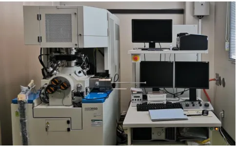
In order to perform in-situ TEM observation and nano-sculpting, in combination with electrical measurements, we have built a custom designed setup, which is illustrated in Figure 2.1. Starting from the left to right, we see a spherical aberration correction software, the TEM microscope (a 50 pm resolved aberration-corrected TEM (JEOL R005) operated at 80 kV and under a pressure of 10-6 Pa) with a TEM holder inserted from the side entry, and the electrical measurement system. The home built TEM holder connect with a source meter (Keithley 2635A) for electrical measurements.
The bias voltage was swept in order from 0.0 to 1.0 V, 1.0 to -1.0 V, and -1.0 to 0.0 V, which corresponded to one cycle, and the current was measured at each 50 mV step.
For obtaining current value accurately and reducing the influence of noise, the output current was programmed to average 10 cycles of the I-V measurement results. The measurement time was dependent on the current value; therefore, the measurement time was not constant. The program was developed by Labview to set the bias voltage and record the measured values.
26
Figure 2.1 Experimental setup: aberration-corrected TEM JEOL R005 with home built holder inside, and the electrical measurement system including Keithley 2635A and the PC with software.
2.2 The design of in-situ TEM holder
Figure 2.2 (a) shows the custom-designed TEM holder, equipped with electrical connections at the bottom. Inside the holder, there are three wires connect the tip, where the specimen is located. Concerning the practical realization of this holder, its design and manufacturing is entirely done in-house, using the facilities provided by the KITANO SEIKI Incorporated.
An enlargement of the TEM holder tip is shown in Figure 2.2 (b): from left to right,
27
it mainly consists of one sample stage, three tungsten probes fixed on one spring-loaded poly-ether-ether-ketone (PEEK) board and three coaxial cables. The sample stage enables us to load a silicon (Si) chip with three different GNR devices.The electrical contact can be established without breaking the Si chip by controllably connecting three tungsten probes with the three electrodes of the GNR devices. Figure 2.2 (c) shows the schematic illustration of the area around the head of the TEM holder with electrical connections. By this design, we realize the measurement of electrical conductance properties with observing the sample in TEM simultaneously.
Figure 2.2 (a) Optical images of home built holder. The black arrow indicate the electrical connections with Keithley 2635A. (b) Enlarged images of the head of holder with sample loaded. (c) Schematic illustration of the area around the head of the TEM holder with electrical connections.
28
2.3 The design of custom TEM chip
The custom TEM chip is a silicon substrate/silicon nitride film (Si/SiN) chip with dimensions of approximately 2.6 × 2.6 mm obtained from SiMPore Incorporated, as shown in the inset of Figure 2.3. It is consisted of a 200-μm-thick silicon wafer covered with a 50-nm-thick SiN film on both sides.
As shown in the Figure 2.3 (a), there are five square windows and three rectangular windows in each chip, which are transparent to electron beam. Those windows are only covered by SiN membrane, which can be used in TEM observation.1,2 From the enlarged SEM images in Figure 2.3(b), the area of each square window and rectangular window is 60 × 60 μm and 500 × 60 μm, respectively. In this experiment, we only designed three tungsten probes for measuring the electrical conductance properties, so only the three central square windows was used for fabrication.
Figure 2.3 (a) Photograph of Si/SiN chip with optical microscopy. (b) SEM image of
29
the initial chip before fabrication process. The enlarged images shows a square window and rectangular window, respectively.
2.4 The fabrication of GNR device
2.4.1 List of equipment used for fabrication
Firstly, we list the main equipment which used for the fabrication of GNR device, and briefly introduce their functions in this experiment.
1. Electron Beam Lithography
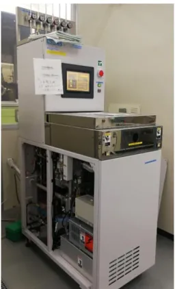
Figure 2.4 Photograph of Electron Beam Lithography machine.
Electron Beam Lithography (EBL, ELS-7500) fabricated by ELIONIX Company.
30
In this experiment, it was used to pattern the designed shape on sample.3 First time, it was used to exposure the electrodes on the Si chip, as describe in Chapter 2.4.3; second time, it was used for patterning the ribbon shapes of graphene, as introduce in Chapter 2.4.5.
2. Reactive Ion Etching system
Figure 2.5 Photograph of Reactive Ion Etching system.
Reactive Ion Etching system (RIE-10NR) fabricated by SAMCO Company. In this experiment, it was used to clean the surface of sample by strong oxygen plasma before
31
electrode fabrication4 in Chapter 2.4.3. In addition, it was also used for etching back layer graphene and exposed graphene in Chapter 2.4.5.
3. Electron Beam Evaporation system (MUE-ECO-EB)
Figure 2.6 Photograph of Electron Beam Evaporation system.
Electron Beam Evaporation system (MUE-ECO-EB) fabricated by ULVAC Company. It was used to deposit the different metals by electron beam evaporation to fabricate the electrodes for devices. In Chapter 2.4.3, chromium/gold (Cr/Au) were deposited by electron beam evaporation on the sample.
32
4. Focused Ion Beam
Figure 2.7 Photograph of Focused Ion Beam machine.
Focused Ion Beam (FIB, SMI-3050) fabricated by HITACHI Company. In Chapter 2.4.4, by using Gallium (Ga) ion beam, we can cut a nano-gap at the center of electrode in our experiment.5,6 The desired dimensions of gap can be controlled by different setting parameters, such as: width, depth and height.
5. Transmission Electron Microscope
33
Figure 2.8 Photograph of Transmission Electron Microscope machine.
Transmission Electron Microscope (TEM, JEM-ARM200F) fabricated by JEOL Company.7 In this experiment, it was used to check the size of gap after using FIB (Chapter 2.4.4) and the fabricated suspended GNRs (Chapter 2.4.5). The acceleration voltage of this machine can be operated at 120 or 200 kV. Since this machine does not have spherical aberration-corrector for TEM mode, it is only used for checking the size of ribbon or taking some low-magnification images.
High resolution TEM images (HR-TEM) of graphene were taken by a 50 pm resolved aberration-corrected TEM (JEOL R005) operated at 80 kV in Tokyo Institute of Technology as shown in Figure 2.1.
34
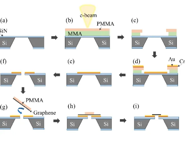
2.4.2 The overall process of fabrication
The fabrication process of suspended GNR device is shown in Figure 2.9, which mainly consists of three steps. The first step is the fabrication of three source-drain electrodes for electrical conductance measurement (Figure 2.9 (a-e)). After the surface of the Si/SiN chip was cleaned with acetone solution, thin Methyl methacrylate (MMA) and poly (methyl methacrylate) (PMMA) resist layers were spin-coated onto the surface of chip and patterned by conventional electron beam lithography (EBL, ELS-7500).
After developing in methylisobutylketone/isopropyl alcohol (MIBK/IPA) to dissolve the exposed PMMA, electron beam evaporated Cr/Au were deposited on the chip at thicknesses of 5 and 40 nm, respectively. Subsequently, N-methyl-2-pyrrolidone (NMP) was used to lift-off the MMA/PMMA layer while leaving the electrodes. The second step is cutting a spatial gapfor suspending the GNR (Figure 2.9 (f)). A gap with a width of 100-300 nm and a length of 2.5 μm was cut at the center of the narrowest electrode by a Ga FIB (SMI-3050), where graphene will be placed. This is essential for TEM observation, the GNR can be directly observed and can be modified in shape and/or size by an intense electron beam. The final step is the transfer and pattering of suspended graphene (Figure 2.9 (g-i)). Large-area graphene grown by chemical vapor deposition (CVD) covered by PMMA layer was directly transferred onto the prepared chip and patterned by using EBL, then followed with O2 plasma etching step (RIE-
35
10NR) to remove the exposed graphene. Finally, the sample was soaked in acetone overnight to completely remove PMMA.8,9 The details of each step will show in the following content.
Figure 2.9 Fabrication steps for producing a suspended GNR device. (a) Initial Si/SiN chip. (b) MMA/PMMA resist layers are spin-coated on the surface of the chip and exposed to an electron beam. (c) The desired electrode pattern is formed by lithography.
(d) Cr/Au films are obtained by electron beam deposition. (e) Lift-off process. (f) A gap is created by an FIB at the center of the electrodes. (g) CVD-grown graphene covered with PMMA is directly transferred onto the Si chip. (h) Graphene is patterned into a
36
nanometer-wide ribbon. (i) A suspended GNR is obtained between two electrodes after O2 plasma etching and acetone cleaning.
2.4.3 Electrodes fabrication
In previous section, we explained the overall process of fabrication GNR devices.
Here we describe in more detail about the fabrication of the Cr/Au electrodes to measure the electrical conductance properties of graphene.
As we mentioned in the last section (Chapter 2.3), the size of TEM grid is very small, which make it difficult to load on a sample stage for spin coating or electron beam exposure process. For fabricating the electrodes on TEM grid, we need to find one method to catch it easily by tweezer and fix it during the fabrication process. For solving this problem, we designed an aluminum (Al) plate for fixing the TEM grid as shown in Figure 2.10. The size of this plate is 20.0 × 15.0 mm, with a thickness of 1.0 mm. At the right side of this plate, there is a hollow of a diamond which corners are rounded. The size of diamond shape is slightly larger than TEM grid for fixing it. The depth is 0.2 mm, which is same with TEM grid. This design will make sure the surface is flat after fixing the grid into Al plate. The round hole below the diamond hollow is used to avoid the damage of SiN membrane during evacuation.
37
Figure 2.10 (a) Photograph of an aluminum plate for fixing the TEM grid. (b) Schematic illustration of the detail design of this plate.
The photograph during the fabrication process are shown in Figure 2.11 (a-f). Firstly, the TEM grid was cleaned with acetone solution and fixed onto Al plate (Figure 2.11 (a,b)). The SiN membrane of TEM grid was so flat that it’s hard to coat with resist layer.
In this case, we tried to make a little roughness of the SiN surface by O2 plasma. After O2 plasma treatment, double layer positive electron-beam resist MMA/PMMA were spin coated on the chip, as shown in Figure 2.11 (c).
EBL was used to pattern the designed electrode shapes. The MMA/PMMA resist was exposed with an electron beam by ELS-7500. After the development in MIBK:IPA solution, the pattern of electrodes could be seen clearly as shown in Figure 2.11 (d).
From the enlarged image in the window, we can confirm the thinnest part of electrode
38
also had been formed. Electron beam evaporator was used to deposit electrodes. After the deposition of Cr/Au metal, an optical photograph of chip of Figure 2.11 (e) shows that all the surface were deposited with metal. Finally, this sample was lift-off with NMP solution for at least 3 hours. During this step, we must take care of the SiN membrane in the window, because it is very fragile. Under this condition, we cannot use ultrasound sonication in this step. The fabricated electrodes on the grid of Figure 2.11 (f) shows three separated source electrodes, a large pad as common drain electrode and some small marks for second time lithography. By this design, we can obtain three individual GNRs on one chip. From an enlarged photograph of the electrode in a small window, the size of thinnest part of electrode is 1.5 μm wide and 20 μm long. All details and setting parameters during this fabrication process has been list in following table 2.1.
39
Figure 2.11 Electrodes fabrication in cleanroom. Photograph of TEM grid after (a) cleaning with acetone solution, (b) fixing on a Al plate, (c) resist coating with MMA/PMMA, (d) electron beam lithography and development, (e) E-beam deposition with Cr/Au, (f) lift off with NMP solution.
40
Table 2.1 List of 1st steps for electrodes fabrication on TEM grid.
1st Step – Electrode fabrication on TEM grid
Step# Step description and detail parameter photograph 1 Cleaning of TEM grid
Clean the grid in those solutions with the turn:
Acetone-IPA-DIW, 3 min for each solution.
Figure 2.11 (a)
2 Fixation of TEM grid on Al plate
Stick grid with PMMA onto the plate, then heating on hot plate at 180 ℃ for 5 min.
Figure 2.11 (b)
3 Making the roughness surface of SiN membrane Using O2 plasma by RIE (10 sccm, 4 min, 100 W, 4 Pa)
- 4 Resist coating with MMA/PMMA double layer
1st layer: MMA copolymer, spincoat 2000 rpm, bake 5 min on hotplate @180°C.
2nd layer: PMMA 495K A4, spincoat 4000 rpm, bake 5 min on hotplate @180°C.
Figure 2.11 (c)
5 Electron beam lithography and development Exposure dose: 300 µC/cm2 with 1nA current.
Develop in MIBK:IPA=1:3, for 2 min, MIBK:IPA=1:1, for 20 sec, rinse 45 sec in IPA.
Figure 2.11 (d)
6 E-beam deposition with Cr/Au
First deposit adhesion layer of Cr, 5 nm with 1.0 A/sec deposition rate, then Au layer, 40 nm at 2.0 A/sec.
Figure 2.11 (e)
7 Lift off with NMP
The sample soaked in NMP for at least 3 hours and lift-off, then clean by IPA solution for 3 min
Figure 2.11 (f)
2.4.4 Fabrication of nano-gaps on the electrode
For TEM observation, graphene must be completely free-standing, which is essential for imaging and sculpting. A gap should be cut on the electrode for separating it to source and drain. Here, we fabricated several gaps with different width and length
41
by using focused ion beam with Ga ion source (SMI-3050).
The TEM images of fabricated gaps are shown in Figure 2.12, the minimum width is 40 nm, and the maximum is 330 nm. After cutting the gap, the electrode was separated from the center. The size of gaps were controlled by the setting parameter during FIB process, which is list in Table 2.2. Although we can fabricate different widths of gap, a narrow size of gap was not suitable for our experiment. There are two reasons: (1).
When the width of gap is very narrow, after transfer CVD-grown graphene, the contact condition between electrodes and graphene is poor, so that the initial contact resistance value is very large. (2). When we clean the surface of GNR by current annealing, the width of gap will change due to high temperature. Under this condition, for narrow gap, the change of width is so large, which makes the ribbon easily rupture due to the stretch force. In conclusion, in the following experiments, we usually fabricate the gaps with the width of 100-300 nm.
42
Figure 2.12 Several fabricated nano-gaps by FIB with the different width of (a) 40 nm, (b) 107 nm, (c) 225 nm, (d) 330 nm, respectively. The black part indicate the Cr/Au electrodes, and the red arrow indicate the measured width of gap.
Table 2.2 List of 2nd steps for cutting nano-gap on electrode.
2nd Step – Nano-gap fabrication on electrode Sample Beam
condition
Length (μm)
Height (μm)
Depth (μm)
Width of gaps (nm)
TEM images
1 Ufine 2.5 0.04 0.25 40 Figure 2.12 (a)
2 Ufine 2.5 0.10 0.20 107 Figure 2.12 (b)
3 Ufine 2.5 0.20 0.20 225 Figure 2.12 (c)
4 Ufine 2.5 0.30 0.20 330 Figure 2.12 (d)
43
2.4.5 Transfer and pattering of graphene
In this part, we focus on the 3rd step: the transfer and pattering of CVD-grown graphene. The CVD graphene grown on copper foil was bought form Graphene Platform Corporation.
As shown in Figure 2.13 (a), a monolayer graphene was grown on 100 mm thick copper foil by CVD method. Figure 2.13 (b) shows the schematic viewing from the cross section. It consists of five layers. From top to bottom, a protect layer, graphene on the top layer, copper foil, graphene on the back layer and heat release sheet.
Figure 2.13 (a) CVD-grown monolayer graphene on 100 mm thick copper foil bought from Graphene Platform Corporation. (b) Schematic of CVD graphene from the cross section.
The transfer method is shown in Figure 2.14. Firstly, the large-area CVD grown graphene on a copper foil was cut to an area of 1 × 1 cm, and peel off the protect layer.
44
Then, a thin PMMA resist layer was spin-coated onto the surface at 4000 rmp, and baked on the hot plate at 180 ℃ for 5 min with peeling off the heat release sheet. The back layer graphene was etched using O2 plasma by RIE (15 sccm, 25 sec, 30 W, 4 Pa).
Subsequently, the PMMA-coated graphene with the copper foil was floated facing down on 5% Ammonium Persulfate solution (APS) to remove the copper foil. For avoiding the copper oxide (CuO) formed during this process, we also make it floated on 50% hydrochloric acid (HCl) solution. Finally, the remaining PMMA-coated graphene was cleaned by deionized water (DIW). The detail time and sequence are list in Table 2.3.
Figure 2.14 Schematic of whole transfer process of graphene onto prepared TEM grid.
45
Table 2.3 List of 3rd steps for preparing transferred graphene.
3rd Step – Preparing the transferred graphene.
Step# Step description Solution Time (min) 1
Cu foil etching
APS 45
2 APS 45
3 APS 45
4 APS 360~
5 CuO etching HCl 10
6 Cleaning DIW 10
7 Cu foil etching APS 10
8 Cleaning DIW 10
9 CuO etching HCl 10
10 Cleaning DIW 10
11 Cleaning DIW 10
12 Cleaning DIW 50~
After etching the Cu foil layer under graphene, it was directly transferred onto the prepared TEM grid and drying for more than 24 h as shown in Figure 2.15 (a). Then the transferred graphene was patterned into nanoribbons by EBL again. The small marks which mentioned in Figure 2.11 (f) were used to adjust the position of ribbon.
They were used for making sure that the patterned GNR just could be fabricated on the cutting gap. After development in MIBK/IPA solution, the optical image of patterned GNRs on the chip is shown in Figure 2.15 (b). Bare SiN film is shown by brown regions on the Si chip; thus, monolayer graphene remained on the chip, except in brown regions.
46
The color results confirmed that the graphene was separated among the three electrodes.
Then exposed graphene was removed by O2 plasma in RIE, as shown in Figure 2.15 (c). From the enlarged image, a narrow ribbon are suspended over the cutting-gap between source and drain electrodes. The size of this suspended GNR was measured at approximately 300 nm wide and 3μm long. Finally, the PMMA layer on graphene was removed by acetone solution. As shown in Figure 2.15 (d), after removing PMMA layer, it’s hard to see the fabricated GNR by optical microscopy even under high- magnification. All the details and parameters during this process are list in Table 2.4.
Figure 2.15 GNR fabrication in cleanroom. Photograph of TEM grid after (a) transfer
47
and drying of graphene, (b) exposure by EBL and development, (c) etching exposed graphene, (d) removing PMMA layer by acetone.
Table 2.4 List of 3rd steps for patterning transferred graphene.
3rd Step –Patterning of graphene
Step# Step description and detail parameter Optical images 1 Drying of the sample
Keep the sample in cleanroom for over 24 h
Figure 2.15 (a) 2 Electron beam lithography and development
Exposure dose: 450 µC/cm2 with 250pA current.
Dose time: 1.8 µs/dot
Develop in MIBK:IPA=1:3 for 3 min, MIBK:IPA=1:1 for 5 sec, rinse 30 sec in IPA.
Figure 2.15 (b)
3 Etching exposed graphene
Using O2 plasma by RIE (10 sccm, 25 sec, 30 W, 4 Pa)
Figure 2.15 (c) 4 Cleaning of PMMA layer
The sample soaked in acetone solution (10 min, 10 min, 6 h~), then clean by IPA solution for 10 min
Figure 2.15 (d)
2.5 Characterization of fabricated GNRs
TEM images were used to check the size and layer number of fabricated GNRs. The low and high magnification images were acquired by JEM-ARM200F under 200 kV.
As shown in Figure 2.16 (a-c), there are three suspended GNRs with different widths between the electrodes. The widths of these ribbons were measured to be 102, 395 and 798 nm, respectively, while the designed widths were 100, 400, and 800 nm, respectively. Thus, the width of the suspended ribbons was well controlled by the
48
exposure conditions. Then, we identified the layer number and checked the quality of GNR by high magnification TEM image. For example, as shown in Figure 2.16 (d), there are many contaminations on the surface of GNR, so it’s hard to obtain the atomic image with the hexagonal structure of graphene underneath them. However, the layer number could be identifiedfrom the corresponding FFT pattern as shown in Figure 2.16 (e). The spots in the FFT pattern correspond to the (100) lattice plane of graphene (0.21 nm), which confirmed that the GNR was a monolayer.
Figure 2.16 TEM images of fabricated suspended GNRs and corresponding electron diffraction pattern. (a-c) TEM images of suspended GNRs with the width of 102, 395, 798 nm, respectively. The black part indicate Au electrodes and red arrows indicate the
49
edge positions of ribbons. (d) High magnification TEM image of a monolayer GNR. (e) The corresponding FFT pattern to (d).
2.6 Conclusion
In this chapter, we have demonstrate the experimental setup and sample preparation.
Firstly, we introduce the equipment and measurement methods used in this experiment.
Then, the design of in-situ TEM holder and custom TEM chip have been explained.
Finally, we showed the fabrication details of the GNR devices, which include the electrodes fabrication, cutting nano-gaps, graphene transfer and patterning. By checking the TEM images, we confirm the suspended monolayer GNRs with the width from ca.100 to 800 nm have successfully fabricated. However, there are some contaminations cover the surface of GNR after fabrication, which influence the observation of atomic structure.
50
References
[1]. Lu, Y.; Merchant, C. A.; Drndic, M.; Johnson, A. T., In situ electronic characterization of graphene nanoconstrictions fabricated in a transmission electron microscope. Nano Letters 2011, 11 (12), 5184–5188.
[2]. Qi, Z. J.; Rodriguez-Manzo, J. A.; Botello-Mendez, A. R.; Hong, S. J.; Stach, E.
A.; Park, Y. W., et al., Correlating atomic structure and transport in suspended graphene nanoribbons. Nano Letters 2014, 14 (8), 4238–4244.
[3]. Vieu, C.; Carcenac, F.; Pepin, A.; Chen, Y.; Mejias, M.; Lebib, A., et al., Electron beam lithography: resolution limits and applications. Applied Surface Science 2000, 164 (1-4), 111–117.
[4]. Tatsumi, T.; Hikosaka, Y.; Morishita, S.; Matsui, M.; Sekine, M., Etch rate control in a 27 MHz reactive ion etching system for ultralarge scale integrated circuit processing. Journal of Vacuum Science & Technology A: Vacuum, Surfaces, and Films 1999, 17 (4), 1562–1569.
[5]. Nagase, T.; Gamo, K.; Kubota, T.; Mashiko, S., Direct fabrication of nano-gap electrodes by focused ion beam etching. Thin Solid Films 2006, 499 (1-2), 279–
284.
[6]. Nagase, T.; Kubota, T.; Mashiko, S., Fabrication of nano-gap electrodes for measuring electrical properties of organic molecules using a focused ion beam.
51
Thin Solid Films 2003, 438, 374–377.
[7]. corrected Microscope, C., JEM-ARM200F.
[Online].Available:https://pdfs.semanticscholar.org/9c21/86bfaa62f1dc8198b0 4db05d0ffa680e6735.pdf
[8]. Rodriguez-Manzo, J. A.; Qi, Z. J.; Crook, A.; Ahn, J. H.; Johnson, A. T.; Drndic, M., In situ transmission electron microscopy modulation of transport in graphene nanoribbons. ACS Nano 2016, 10 (4), 4004–4010.
[9]. Wang, Q.; Kitaura, R.; Suzuki, S.; Miyauchi, Y.; Matsuda, K.; Yamamoto, Y., et al., Fabrication and in situ transmission electron microscope characterization of free-standing graphene nanoribbon devices. ACS Nano 2016, 10 (1), 1475–1480.
52
Chapter 3 Graphene cleaning methods
Introduction
This chapter introduced several different methods for cleaning the surface of graphene nanoribbon. Including: dry-cleaning with adsorbents (heating with active carbon), heating in vacuum by using a heating holder, heating in gas environment (Ar/H2), and in-situ current annealing (Joule heating). By checking the cleanliness of GNR from high-resolution TEM images, we compared the above cleaning methods and found the most suitable and effective method.
53
3.1 Consideration on cleaning of graphene
The properties of graphene have proved to be very sensitive to the surface contamination, which degrade the excellent optical and electrical conductance properties of graphene.1, 2 Residues on the surface of graphene also result in an unintended doping effect and unstable electrical performance due to nonuniform charge accumulation at the interface between the electrode material and graphene.3 So achieving ultraclean graphene samples is a key issue for investigating the intrinsic electrical conductance properties of graphene. Unfortunately, polymeric residues, impurity particles and other contaminants are easily involved during the lithography process, which is essential for the fabrication of GNR devices. The surface contaminants are typically composed of hydrocarbons with wide variation in their stoichiometry (C = O, C-OH, or H-C) and chain lengths.4 Such contamination can be cross-linked and/or graphitized under the electron beam of a TEM5 or at high temperatures.6, 7 It is therefore considerably difficult to obtain an ultraclean graphene sample. In order to reduce the contamination on the graphene, cleaning is usually recommended after the fabrication1, 8-10.
Until now, various treatments have been used for cleaning the surface of graphene, such as: heating treatment in a vacuum or gas environment, dry-cleaning with adsorbents, plasma etching, in-situ current annealing and so on. Heating treatment is
54
one of the most common methods for removing hydrocarbon contamination from surfaces. Although annealing of graphene in vacuum or inert atmosphere reduces the amount of contamination,11, 12 it has been shown that residuals are still present after such treatment.13 If the heating is insufficient, many contaminants will remain; if the sample is over-heated, obvious defects may occur, especially for the suspended graphene. This will hinder the investigation of the intrinsic properties of graphene.
Recently, a different approach for cleaning graphene was developed: the use of a metal-catalyst (Pt or Pd) to aid in the removal of surface contamination14 on graphene.
Although this method can remove efficiently contamination from graphene at moderate temperatures (300℃) and under atmospheric conditions. However, depositing metals on the sample surface is not desirable, especially for our fabricated GNR devices which are used for electronic applications.
Since it is difficult to find a uniform and proper cleaning condition for specific graphene devices, especially for suspended GNRs, we will try several different cleaning methods and find the most suitable one for our devices in this chapter.
3.2 Dry-cleaning with adsorbents
Here, we present a special cleaning method, dry-cleaning with adsorbents which has been reported in 2014.15 They observed surface cleanness of 95% in single layer
55
graphene, when embedding free-standing single-layer graphene supported on Quantifoil TEM grids in commonly used adsorbents-activated carbon (Merck,
“charcoal activated for analysis”). It seems that this method is very simple and effective.
Following their method, we tried to clean the surface of GNR which fabricated on TEM grid. For comparison, we tried to clean two different types of sample. One sample is transferred graphene on typical copper TEM-grid, another one is custom Si/SiN grid with fabricated GNRs. Both of them were embedded in a powder of activated carbon inside a glass vial. Then, this vial was placed on a hot plate, which was heated from room temperature to ~210℃ at a rate of 5 ℃/min. The sample was held at this temperature for 30 min. Afterwards, these sample were cooled to room temperature and blown gently with air before inserting them in the TEM to remove remaining active carbon from the surface of the samples.
As shown in Figure 3.1, it shows the TEM images of these two samples before and after cleaning process, which were took by ARM-200F at 200 kV. Figure 3.1 (a-c) shows the TEM images of transferred graphene on copper foil before and after heating with active carbon. The sample surface covered with contamination with only small patches of clean graphene as shown in Figure 3.1 (a), which is a typical non-cleaned graphene sample. After dry-cleaning with active carbon, the cleanness is improved, as shown in Figure 3.1 (b). From an enlarged TEM images Figure 3.1 (c), the clean area