Japan Advanced Institute of Science and Technology
JAIST Repository
https://dspace.jaist.ac.jp/Title
Unusually large absolute Raman scattering cross
section of hydrogen vibrations on Si(111)
Author(s)
Sano, H.; Ushioda, S.
Citation
Physical Review B, 53(4): 1958-1962
Issue Date
1996-01-15
Type
Journal Article
Text version
publisher
URL
http://hdl.handle.net/10119/4406
Rights
H. Sano and S. Ushioda, Physical Review B, 53(4),
1996, 1958-1962. Copyright 1996 by the American
Physical Society.
http://link.aps.org/abstract/PRB/v53/p1958
Description
Unusually large absolute Raman scattering cross section of hydrogen vibrations on Si
„111…
H. Sano*and S. UshiodaResearch Institute of Electrical Communication, Tohoku University, Sendai 980-77, Japan
~Received 2 May 1995!
We have measured the absolute Raman scattering cross section of the terrace vibration mode of silicone-monohydride on a Si~111! surface that was prepared by chemical etching in a NH4F solution. The measured
cross section at the incident wavelength of 4880 Å is (dszz/dV)5(8.3760.32)310228cm2/~sr line Si-H
bond!. It is about 74 times the cross section of the symmetric stretching mode of the gaseous SiH4molecule.
The measured excitation profile of the cross section in the range oflin54579–5145 Å has av4dependence
indicating that there is no resonant enhancement of the cross section. We estimate that the Raman transition dipole matrix elements are about three times larger for the Si~111!/H monolayer system than for the free SiH4molecule.
I. INTRODUCTION
Raman scattering is a powerful tool for investigations of molecular vibrations. However, its surface sensitivity is ap-preciably lower compared with infrared absorption spectros-copy and electron-energy-loss spectrosspectros-copy~EELS!. Thus it has been extremely difficult to detect weak Raman scattered light from a monolayer adsorbed on solid surfaces, except in cases where surface-enhanced Raman scattering ~SERS! occurs1 or electronic resonances enhance Raman intensities.2,3Only a few examples of successful observation of ‘‘unenhanced’’ Raman scattering from a monolayer have been reported; e.g., nitrobenzene, pyridine, and benzene on Ag and Ni by Campion and co-workers4 – 6and nitrobenzene on Ni by Chou et al.7
Recently Hines et al.8 have observed the Raman spectra of the Si-H stretching vibrations on a H-terminated Si~111! surface with an unusually high signal-to-noise ratio. Their results suggest that the Raman scattering cross section of the Si-H stretching mode is unusually large. There are only a few reports on the SERS effect on semiconductor surfaces,9–11 and in particular no report of SERS on Si surfaces. Thus the strong Raman scattering by less than a monolayer of H on Si observed by Hines et al. is very intriguing. The question is what enhances the Raman intensity so much in this sample system.
As a first step toward understanding the mechanism that causes the unusually large Raman signal from the Si-H sys-tem, we have measured the absolute Raman scattering cross section of this mode. We then examined various possible enhancement mechanisms.
II. EXPERIMENT
The sample substrates were B-doped p-type Si~111! with resistivity r57 –7.5 V cm and Si~100! with r51.3–1.7
V cm. The substrates were prepared in a clean room by the
following steps using high-grade reagents and purified con-tainers suitable for silicon device processing:~1! Two cycles of cleaning in a hot solution of 97% H2SO4:30% H2O25
4:1~5 min! and rinsing with high-purity deionized ~DI! water
~4 min!. ~2! Etching in a 1% HF solution and rinsing with DI
water ~4 min!. ~3! Reoxidizing in a hot solution of 97% H2SO4:30% H2O254:1 ~5 min!, and rinsing with DI water
~4 min!. ~4! Etching in a 40% NH4F solution ~90 s! and
rinsing with DI water ~4 min!. ~5! Reoxidizing in a hot so-lution of 97% H2SO4:30% H2O254:1 ~5 min! and rinsing
with DI water~6 min!. ~6! Etching in a 40% NH4F solution
~3 min!. ~7! Rinsing with DI water ~10 s! and venting with
dry N2 gas.
For one of the Si~111! substrates, a different sample preparation method was also used: etching in a 1% HF solu-tion ~3 min! instead of the last etching process ~6! in a 40% NH4F solution~3 min!.
Studies by scanning tunneling microscope ~STM! ~Refs. 12–14! and multiple internal reflection absorption spectros-copy~MIRAS! ~Refs. 15 and 16! have shown that the surface morphology and the surface-adsorbed species after etching processes depend on the crystal orientation of the Si surface and the pH of the HF solution. These results can be ex-plained by the extremely low etching rate along the @111# direction by a high-pH HF solution. From the results re-ported in Refs. 12–16, we can say with fair certainty that the three kinds of samples we prepared have the surface proper-ties described below.
Sample A: Etched Si~111! in a 40% NH4F solution~pH of 7.8! in the last stage of sample preparation. This sample has an atomically flat and ideally monohydride-terminated~111! surface.
Sample B: Etched Si~111! in a 1% HF solution ~pH of 2! in the last stage of sample preparation. This surface is uni-formly covered with atomic scale roughness. There are dihy-drides and trihydihy-drides in addition to monohydihy-drides on the surface.
Sample C: Etched Si~100! in a 40% NH4F solution~pH of 7.8! in the last stage of sample preparation. This surface is rough like sample B and has etch pits. Various species, i.e., monohydrides, dihydrides, and trihydrides, exist on the sur-face.
The Raman spectra were measured immediately after the sample preparation, using an argon-ion laser as the incident light source. The incident wavelengths and the incident power were as follows: For sample A, 4579 Å ~83 mW!, 4765 Å ~265–290 mW!, 4880 Å ~400–408 mW!, and 5145 53
Å ~397–413 mW!; and for samples B and C, 4880 Å ~400 mW!. The incident angle was 60° from the surface normal, and the polarization was parallel to the plane of incidence ( p polarized!. To lower the power density on the sample surface, the laser beam was focused with a cylindrical lens to form an elliptical spot of roughly 233 mm on the surface. The scattered light was collected in a direction 60° from the surface normal in a plane rotated by 20° from the incident plane. The solid angle of collection wasDV52.8431022sr. The spectrometer is a Jobin-Yvon U-1000 double monochro-mator equipped with a Hamamatsu R649 photomultiplier tube. The absolute sensitivity of this spectrometer system hsys has been calibrated as a function of wavelength and
polarization by using a standard halogen lamp.17 Thus the observed photon counting rate can be directly converted to absolute intensity. The cross section of the Si-H stretching vibration mode at;2085 cm21was measured in air at room temperature. To suppress the Raman scattered background due to the atmospheric N2 centered at;2330 cm21, argon gas was blown at the sample surface.
III. ANALYSIS OF THE RAMAN CROSS SECTION OF ADSORBED MOLECULES
In this section we present the necessary formulas for cal-culations of the absolute Raman scattering cross section of adsorbed molecules. To obtain the absolute Raman cross sec-tion of surface-adsorbed molecules that can be compared with that of the isolated gaseous molecules, it is necessary to account for the effects of the presence of the substrate on the propagation of the incident and scattered light. We consider the Raman scattering process by surface-adsorbed molecules in three steps: ~1! Generation of the local macroscopic elec-tric field at the molecular site by the incident light.~2! Gen-eration of the Raman dipole by the local field through the Raman tensor.~3! Propagation of the scattered light from the Raman dipole. This approach to the Raman scattering pro-cess by surface-adsorbed molecules has been described in detail by Sakamoto, Mizutani, and Ushioda.17 We follow their analysis for the absolute cross section.
To analyze the specific sample configuration at hand, we adopt the three layered dielectric model that was used by Hines et al.8In this model the three layers consist of a semi-infinite Si substrate, an semi-infinitely thin Si-H adsorbate layer, and a semi-infinite vacuum above. The adsorbate layer is assumed to have an isotropic real dielectric constant «ads.
All interfaces are assumed to be flat.
From Eq. ~9! of Ref. 17 the Raman scattering intensity from an adsorbed molecule can be expressed by
Iout5
S
vs cD
4S
«n~vs! «n~vin!D
1/2 Iin Abeam 3ueoutAT~u s,fs,vs!aLA~uin,fin,vin!einu2, ~1!where the symbols are defined as follows: Ioutis the Raman scattering intensity per unit solid angle. Iinand Abeamare the
total intensity and the illuminated area by the incident light, respectively. c is the speed of light in vacuum.vinandvsare
the frequencies of the incident and scattered light, respec-tively. «n is the dielectric constant of the top layer that is
vacuum in our system. Thus @«n(vs)/«n(vin)#1/2 becomes
unity. einand eoutare the incident and scattered polarization vectors, respectively. The angles uj andfj ( j5in or s! are the directions of the incident and scattered light. aL is the 333 Raman tensor of the scattering molecule. All Si-H bonds of the ideal Si~111! surface are directed along the z axis defined along the surface normal. Since a Si-H bond can be regarded as an isolated diatomic molecule, the Raman tensor of a Si-H bond takes the form
aL5a zz L
S
d 0 0 0 d 0 0 0 1D
~2!by symmetry.d is the bond anisotropy defined by the ratio of the molecular polarizabilities perpendicular and parallel to the bond axis. Hines et al.8have already determinedd of the Si-H bond on Si~111! by measuring the polarization depen-dence of the Raman intensity. We use their value of d50.263 for the present analysis. A is the matrix that
de-scribes the propagation of the incident wave near the sub-strate surface and determines the incident local field in the adsorbate layer. This matrix A consists of the electromag-netic Green’s function of a layered structure that is described in detail in Ref. 18. AT is the transpose of A.
In actual Raman measurements, experimental parameters such as the sensitivity of the spectrometer system (hsys) and
the solid angle of collection (DV) enter the observed Raman intensity. To include these experimental parameters, we use the following equation derived from Eq. ~1!:
Nobs5hsysDVrs vs 3 vin c4 ue outATaLAeinu2N in 5hsysDVrs
S
dszz dVD
gNin, ~3! whereS
dszz dVD
[ vs 3 vin c4 uazz Lu2, ~4! g5U
eoutATS
d 0 0 0 d 0 0 0 1D
AeinU
2 . ~5!The symbols in Eq. ~3! are defined as follows: Nobsis the
observed total photon number of Raman scattered light for a given vibrational mode. Nin is the total number of incident photons.rsis the surface density of the Si-H bonds.
Assum-ing that the Si~111! surface is perfectly terminated by hydro-gen monohydride, the surface density rs is equal to that of
the Si atoms on Si~111!, which is 7.8331014 cm22. (dszz/dV) is the quantum Raman scattering cross section
defined as the ratio of the number of scattered photons per Si-H bond to the number of incident photons per unit area. The unit of the cross section is cm2/~sr line Si-H bond!.g is
the correction factor that arises from the effect of the local electric field. For the calculation of g we use the dielectric constant of bulk Si ~Ref. 19! and the dielectric constant of the adsorbate layer («ads53.78) that was obtained by Hines
et al.8We can calculate the absolute Raman scattering cross section from the measured absolute intensity using Eq. ~3!.
IV. RESULTS
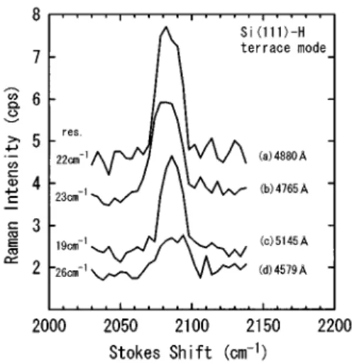
For samples B and C no Raman peak for the stretching vibration of monohydride, dihydride, and trihydride was ob-served. For sample A a Raman peak was clearly observed at
;2085 cm21, as shown in Fig. 1. The Raman spectra in Fig.
1 are uncorrected bare data. The peak at ;2085 cm21 is assigned to the in-phase terrace vibration of monohydrides on Si~111!.8The results from MIRAS~Ref. 20! show that the natural linewidth of this terrace mode is inherently less than 1 cm21at room temperature. The observed linewidth of the peak in Fig. 1 agrees with the instrumental resolution that is determined by the slit width of the monochromator. For sample A no stretching vibration modes ~2106–2140 cm21) assigned to the dihydride and trihydride vibrations were observed.
Figure 2 shows the incident wavelength dependence of the absolute Raman scattering cross section of the Si-H ter-race mode. The open circles are the data points. The error bars are estimated from the statistical fluctuation
A
N of theRaman peak photon number N. The solid curve is the calcu-lated v4 dependence. It is fitted to the data points by the method of least squares. The data points agree very well with the v4 curve. From this fitting, the absolute Raman scatter-ing cross section of the terrace vibration mode at the incident wavelength of 4800 Å is
S
dszzdV
D
5~8.3760.32!310228 cm22/~sr line Si-H bond!,
~6!
where 60.32 is the uncertainty determined by the mean-square fitting.
V. DISCUSSION
The absolute Raman scattering cross section of the terrace vibration of monohydrides on Si~111! that we obtained above is greater than most of the known absolute cross sections of gaseous molecules.21 For example, it is interesting to com-pare the present result with the Raman cross section of the symmetric stretching vibration ~n1, 2185.7 cm21) of the
SiH4 molecule in the gaseous state:
S
dsdV
D
51.13310229 cm2/~sr molecule!; ~7!
that is, the quantum cross section derived from the power cross-section at the incident wavelength of 4880 Å in Ref. 22. Although we are looking at the same stretching vibration of the Si-H bond, the cross section of the Si-H terrace mode is about 74 times greater than that of the Si-H stretching mode of SiH4.
Now let us consider the mechanisms that can possibly cause the observed difference between the cross sections of the Si-H terrace mode and the stretching mode of SiH4. Possible candidate mechanisms that we have considered are
~1! enhancement of the local electric field due to surface
roughness~similar to SERS!, ~2! resonance due to electronic transitions, and~3! larger dipole transition matrix elements.
On rough surfaces or island films of metals, especially of silver, surface plasmons~SP’s! are resonantly excited by the incident light and the excitation of the SP’s enhances the local electric field at the site of the adsorbed molecule.1,23 This enhancement effect is believed to be operative in SERS,1but the presence of surface roughness is essential for this mechanism to be effective. In the case of semiconductor surfaces, the SERS enhancement mechanism is weak in com-parison with the metallic case. For fine GaP particles with diameters of 400–1000 Å, the enhancement factor of a few hundred11has been reported. The surface of sample A in the present study is extremely smooth, and the necessary rough-FIG. 1. Raman spectra of the terrace vibration mode of
mono-hydride on Si~111! etched in a NH4F solution for different incident
laser wavelengths. ~a! Incident power Iin5408 mW, accumulation
time/point Tacc5175 s. ~b! Iin5266 mW, Tacc5150 s. ~c! Iin5410
mW, Tacc5140 s. ~d! Iin583 mW, Tacc5150 s. The energy
resolu-tion for each spectrum is indicated on the left.
FIG. 2. Absolute Raman cross section of the Si-H terrace vibra-tion mode as a funcvibra-tion of the wavelength of the incident light. The open circles are the experimental data points. The solid curve is a root-mean-squared fit to av4curve. The unit of the absolute Raman cross section, corresponding to the vertical axis, is cm2/~sr line Si-H
ness does not exist on the surface. Hence the enhancement of the Raman intensity due to the resonant excitation of SP’s cannot be expected. This conclusion is supported by the re-sult that no Raman peak in samples B and C was observed, although the surface roughness of samples B and C is greater than that of sample A.
When the energy of the incident and/or scattered light lies close to the energy of the electronic transitions of the ad-sorbed molecules, the Raman scattering cross section is en-hanced due to resonance.24 The energy levels of the mono-hydride on Si~111! have been investigated by ultraviolet photoemission spectroscopy ~UPS! measurements and theo-retical calculations.25–27 Their results show that for the monohydride the highest filled state is located about 4.5 eV below the Fermi level, and the lowest empty state is located about 3 eV above the Fermi level. Thus the absorption due to the optical transitions of the Si-H bond is expected to have a peak in the range of 7– 8 eV.27 Since the energy of the inci-dent photons in the present Raman study is much smaller than that of this optical transition, the enhancement of the Raman intensity by resonance cannot be expected. The ex-perimental result shown in Fig. 2 also confirms this conclu-sion. The excitation profile of the Raman scattering cross section in Fig. 2 shows a v4 dependence without any
indi-cation of electronic resonances.
From the above considerations we see that the first two enhancement mechanisms of the Raman scattering cross sec-tion are not operative in the present situasec-tion. Thus we must conclude that the dipole matrix elements that enter the Ra-man cross section for the Si~111!/H system is larger than those for the free SiH4 molecule. This means that the
elec-tronic wave function of the Si-H bond in the Si~111!/H sys-tem is significantly different form that found in the SiH4
molecule. The expression for the Raman polarizability con-sists of the sum of terms that contain two dipole transition matrix elements in the numerator. Hence, roughly speaking, the Raman polarizability is proportional to the square of
typi-cal dipole matrix elements, and the Raman cross section in turn is proportional to the fourth power of the dipole matrix elements. To account for a factor of about 80 in the Raman cross section, one needs a factor of 3 in the size of the dipole matrix elements. A change in the size of dipole matrix ele-ments of a factor of 3 due to the difference in the nature of the bonds between the Si~111!/H system and the free SiH4
molecule seems to lie within a reasonable range. To under-stand the difference in detail, it is necessary to perform a theoretical calculation of the Raman polarizability for the two systems.
VI. CONCLUSION
We have measured the absolute Raman scattering cross section of the Si-H terrace vibration mode on Si~111!. The cross section is larger than most of the cross sections of free gaseous molecules, and is about 74 times that of the sym-metric stretching vibration of SiH4. The usual enhancement mechanisms of Raman cross sections, such as enhanced local electric fields due to surface roughness and electronic reso-nances, cannot explain the large difference in the cross sec-tions between the monolayer of Si-H on Si~111! and the free SiH4 molecules. At present, we conclude that the relevant
electronic wave functions of the Si-H monolayer is signifi-cantly different from those of the free SiH4 molecule. We estimate that the Raman transition dipole matrix elements are about three times larger for the Si~111!/H monolayer system than for the free SiH4 molecule.
ACKNOWLEDGMENTS
One of us~S.U.! would like to acknowledge valuable dis-cussions with M. A. Hines and Y. J. Chabal. This work was supported in part by a Grant-in-Aid for Scientific Research from the Ministry of Education, Science, and Culture. We gratefully acknowledge financial assistance from the Taka-hashi Science Foundation.
*Present address: School of Materials Science, Japan Advanced
In-stitute of Science and Technology, Tatsunokuchi-machi, Nomi-gun, Ishikawa 923-12, Japan.
1A good general review of the experimental and theoretical work
on SERS has been given by A. Otto, in Light Scattering in Solids IV, edited by M. Cardona and G. Gu¨ntherodt~Springer-Verlag, Berlin, 1984!, Chap. 6, pp. 289–418.
2J. D. Jiang, E. Burstein, and H. Kobayashi, Phys. Rev. Lett. 57,
1793~1986!.
3N. Esser, M. Ko¨pp, P. Haier, and W. Richter, J. Electron
Spec-trosc. Relat. Phenom. 64/65, 85~1993!.
4A. Campion, J. K. Brown, and V. M. Grizzle, Surf. Sci. 115, L153
~1982!.
5A. Campion and D. R. Mullins, Chem. Phys. Lett. 94, 576~1983!. 6D. R. Mullins and A. Campion, J. Phys. Chem. 88, 8~1984!. 7C.-C. Chou, C. E. Reed, J. C. Hemminger, and S. Ushioda, J.
Electron Spectrosc. Relat. Phenom. 29, 401~1983!.
8M. A. Hines, T. D. Harris, A. L. Harris, and Y. J. Chabal, J.
Electron Spectrosc. Relat. Phenom. 64/65, 183~1993!.
9H. Yamada and Y. Yamamoto, Surf. Sci. 134, 71~1983!. 10J. E. Potts, R. Merlin, and D. L. Partin, Phys. Rev. B 27, 3905
~1983!.
11S. Hayashi, R. Koh, Y. Ichiyama, and K. Yamamoto, Phys. Rev.
Lett. 60, 1085~1984!.
12G. S. Higashi, R. S. Becker, Y. J. Chabal, and A. J. Becker, Appl.
Phys. Lett. 58, 1656~1991!.
13Y. Morita and H. Tokumoto, in Interface Control of Electrical,
Chemical, and Mechanical Properties, edited by S. P. Murauka, T. Ohmi, K. Rose, and T. Seidel, MRS Symposia Proceedings No. 318~Materials Research Society, Pittsburgh, 1994!, p. 293.
14Y. Morita, K. Miki, and H. Tokumoto, Appl. Surf. Sci. 60/61, 466
~1992!.
15P. Jakob and Y. J. Chabal, J. Chem. Phys. 95, 2987~1991!. 16P. Dumas, Y. J. Chabal, and P. Jakob, Surf. Sci. 269/270, 867
~1992!.
17K. Sakamoto, G. Mizutani, and S. Ushioda, Phys. Rev. B 48,
8993~1993!.
18C. E. Reed, J. Giergiel, J. C. Hemminger, and S. Ushioda, Phys.
Rev. B 36, 4990~1987!.
19D. F. Edwards, in Handbook of Optical Constants of Solids,
ed-ited by E. D. Palik~Academic, New York, 1985!, pp. 547–569.
20P. Dumas, Y. J. Chabal, and G. S. Higashi, Phys. Rev. Lett. 65,
1124~1990!.
21H. W. Schro¨tter and H. W. Klo¨ckner, in Spectroscopy of Gases
and Liquids, edited by A. Weber~Springer-Verlag, Berlin, 1979!, Chap. 4.
22R. S. Armstrong and R. J. H. Clark, J. Chem. Soc. Faraday Trans.
II 72, 11~1976!.
23G. W. Ford and W. H. Weber, Phys. Rep. 113, 195~1984!. 24B. B. Johnson and W. L. Peticolas, Ann. Rev. Phys. Chem. 27,
465~1976!.
25J. E. Rowe, Surf. Sci. 53, 461~1975!.
26K. M. Ho, M. L. Cohen, and M. Schlter, Phys. Rev. B 15, 3888
~1977!.