Reducibility of Sequential Test Generation to Combinational Test Generation for
Several Delay Fault Models
Tsuyoshi Iwagaki Satoshi Ohtake Hideo Fujiwara Graduate School of Information Science, Nara Institute of Science and Technology
Kansai Science City 630-0192, Japan E-mail: tsuyo-i, ohtake, fujiwara @is.aist-nara.ac.jp
Abstract
This paper presents a new structure, called discontinu- ous reconvergence structure (DR-structure), of sequential circuits with easy testability for delay faults. We show that the delay fault test generation problem for sequen- tial circuits with DR-structure can be reduced to that for their time-expansion models, which are combinational cir- cuits. Based on the reducibility, we propose a test genera- tion method for delay faults in sequential circuits with DR- structure. This method can be applied to several delay fault models. By some experiments, we show that the proposed method is effective in the hardware overhead, the test gen- eration time and the fault efficiency.
1 Introduction
As the speed of modern VLSI circuits reaches the giga- hertz range, delay testing is becoming essential. Until now, several delay fault models have been investigated [8]. The path delay fault model [11] is one of the most general mod- els among them because distributed faults along paths can be tested and the delay size of detectable faults is scalable.
Test generation for sequential circuits under simple fault models such as the single stuck-at fault model is itself gen- erally a hard task. Delay test generation for sequential cir- cuits is a more challenging problem. For such sequential circuits, design for testability (DFT) is an important ap- proach to reduce the test generation effort. Given a sequen- tial circuit, a fully enhanced scan technique [3] replaces each flip-flop (FF) by an enhanced scan FF (ESFF). An ESFF can store two bits to apply two consecutive vectors. For a sequential circuit designed by this technique, we can use a combinational delay fault test generation algorithm (ATPG) to generate test sequences. Therefore, high fault coverage can be achieved with short test generation time. However, hardware overhead caused by extra memory ele- ments of ESFFs is very high. It can be alleviated by using partial scan techniques [1, 10]. In a partially enhanced scan technique [1], for a sequential circuit, FFs to be replaced with ESFFs are selected such that feedback paths in the cir- cuit are broken if these FFs are removed. For a sequential circuit designed by this partial scan technique, we can con- sider the circuit to be a feedback free circuit during test gen- eration, and test generation for the feedback free circuit is easier than that for the original circuit. However, there is room for facilitating test generation because it still requires
a sequential delay fault ATPG. We have proposed a partially enhanced scan design method [10]. The method is based on balanced structure [4]. The class of acyclic sequential circuits properly includes that of balanced sequential cir- cuits. We showed that test sequences for path delay faults in balanced sequential circuits can be generated by applying a combinational delay fault ATPG to their combinationally equivalent circuits. Thus, our prior method can ease delay test generation complexity at the cost of a large number of ESFFs compared with the method [1]. In this paper, we dis- cuss an extended class of sequential circuits for which test sequences can be generated by a combinational delay fault ATPG.
This paper presents a new structure, called discontinuous reconvergence structure (DR-structure), of sequential cir- cuits. The relation among three classes of sequential circuits is as follows: the class of acyclic sequential circuits
the class of sequential circuits with DR-structure the class of balanced sequential circuits . DR-structure has a property of easy testability for delay faults: test sequences for delay faults in sequential circuits with DR-structure can be generated by applying a combinational delay fault ATPG to their equivalent combinational circuits. For acyclic se- quential circuits, notation of time-frames [9] and notation of time-expansion models [6] have been proposed as ways to denote equivalent combinational circuits. In this paper, we employ time-expansion models as notation of equiv- alent combinational circuits, and show the reducibility of test generation for delay faults in a sequential circuit with DR-structure to that for the corresponding delay faults in its time-expansion model. Based on the reducibility, we pro- pose a delay test generation method for sequential circuits with DR-structure. By experiments, we confirm the follow- ing: test generation time can be reduced and fault efficiency can be enhanced by using our method instead of an ordi- nary method using a sequential delay fault ATPG. In order to apply the proposed method to general sequential circuits, we use a partially enhanced scan technique. Theoretically, DR-structure can be extracted from the circuits with low hardware overhead compared with balanced structure. In this paper, we also confirm it experimentally.
2. Preliminaries
In general, a sequential circuit consists of combinational logic blocks (CLBs) connected with each other directly or IEEE the 12th Asian Test Symposium (ATS'03), pp.58-63, Nov. 2003.
1
3 4 2
5 I1 6
I2 O
1 1
1 1
1
2 0
1 0 0
0 I1
I2
1 2
4
3 5
6 O (a)
(b)
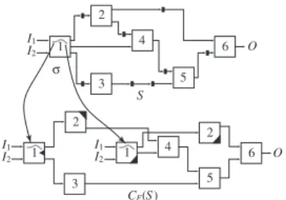
Figure 1. (a) Sequential circuit: S; (b) Topol- ogy graph of S: G.
through FFs. A CLB in the circuit is a region of con- nected combinational logic. The circuit can be modeled by a weighted directed graph defined as follows.
Definition 1 The topology graph for a sequential circuit S is a weighted directed graph G V A w, where
Vis the set of vertices representing primary inputs, pri- mary outputs and CLBs in S,
A V Vis the set of arcs representing FFs and wires in S, and
w: A 0 N, where N is the set of natural numbers, defines the weights of the arcs, and w u v (u v V) denotes the number of FFs on a connection u v A. Example 1 Examples of a sequential circuit and its topol- ogy graph are shown in Figure 1. In Figure 1(a), 1 2 6 are CLBs, and black blocks are FFs.
In this paper, we assume that FFs have no hold capa- bility, and those are of D-type. This assumption does not impose restriction on circuit representation because any FF with hold capability or the other types of FFs can be mod- eled by a D-type FF and some logic gates.
2.1. Target fault models
In this paper, we consider three delay fault models: the path delay fault model, segment delay fault model and tran- sition fault model. However, in the remaining paper, we focus on the segment delay model because it can repre- sent both the path delay fault model and the transition fault model.
In a circuit, a segment is defined as an ordered set of gates g1 g2 gL, where L is the length of the segment, and gate gi is an input to gate gi 1 (1 i L 1). The length of the segment, L, can be anywhere from 1 to Lmax, where Lmax represents the number of gates in the longest path in the circuit. A segment has a delay fault if propaga- tion time of rising or falling transition through the segment exceeds a specified limit. Such a delay fault on a segment is said to be a segment delay fault (SDF) [5]. It is assumed that a segment delay fault is large enough to cause delay faults on all paths that include the segment. In test generation for the segment delay fault model, the fault list consists of all segments whose length is L and all paths whose length is less than L. When L 1, the segment delay fault model re- duces to the transition fault model. When L Lmax, it is equivalent to the path delay fault model [5].
Next, we define the testability of an SDF in both sequen- tial circuits and combinational circuits.
Definition 2 Let S and s be a sequential circuit and a seg- ment in S, respectively. Let f and Sf be the SDF on s and the faulty circuit of S with f , respectively. Let C be the combinational circuit composed of all the CLBs on s, and let t be a specified clock period of S. In a slow-fast-slow testing[8], f is testable if there exists an input sequence T for S and Sfsuch that the following conditions hold.
1. By applying an input vector pair v1 v2 to C, the de- sired transition is launched at the starting point of s, and the transition is propagated to the ending point of salong s. Then, at time t, the value induced by v2at the ending point in Sf is different from that in S. 2. By applying T to Sf, v1 v2 is justified to C, and the
fault effect of f at the ending point is propagated to a primary output.
Such an input sequence T is regarded as a test sequence for f.
In this paper, we assume a slow-fast-slow testing strategy in test application because a sequential circuit can be con- sidered delay fault-free in both the fault initialization and the fault effect propagation phases.
Definition 3 Let C and s be a combinational circuit and a segment in C, respectively. Let f and Cf be the SDF on s and the faulty circuit of C with f , respectively. Let t be a specified limit time. The fault f is testable if there ex- ists an input vector pair v1 v2 for C and Cf such that the following conditions hold.
1. By applying v1 v2 to C and Cf, the desired transition at the starting point of s is launched, and the transition is propagated to the ending point of s along s. Then, at time t, the value induced by v2at the ending point in Cfis different from that in C.
2. The fault effect of f at the ending point is propagated to a primary output by applying v1 v2 to Cf. Such an input vector pair v1 v2 is regarded as an two- pattern testfor f .
2.2. Transformations
In the test generation method proposed in Section 4, test sequences for delay faults in sequential circuits with DR- structure are generated by applying a combinational ATPG to their equivalent combinational circuits. In this paper, we employ time-expansion models [6] as notation of equiva- lent combinational circuits. A time-expansion model for an acyclic sequential circuit is defined based on the following time-expansion graph[6].
Definition 4 Let S be an acyclic sequential circuit, and let G V A w be the topology graph of S. Let E
VE AE t l be a directed graph, where VE is the set of ver- tices, AE is the set of arcs, t is a mapping from VE to the set of integers, and l is a mapping from VE to V . If E sat- isfies the following four conditions, E is said to be a time- expansion graph (TEG)of G.
C1 (CLB preservation) The mapping l is surjective, i.e., v V u VEs.t. v l u .
C2 (Input preservation) Let u be a vertex in E. For any direct predecessor of l u in G, v pre l u , there ex- ists a vertex u in E such that u pre u and l u v, where pre x is the set of direct predecessors of a ver-
4 3
I1
I2
1 I1
I2
1 2 2
5 6 O 2
1 3
0 4
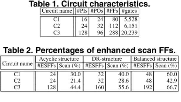
Figure 2. Time-expansion graph of G: E.
3
4 2 2
5
6 O
I1 1 I2
I1 1 I2
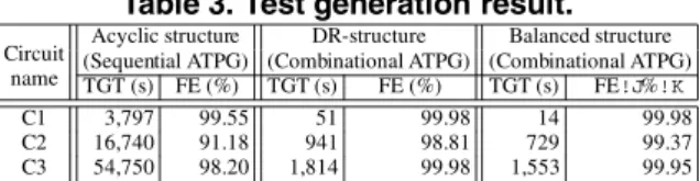
Figure 3. Time-expansion model of S based on E: CE S.
tex x.
C3 (Time consistency) For any arc u v AE, there ex- ists an arc l u l v A such that t v t u w l u l v .
C4 (Time uniqueness) For any vertices u v VE, if t u t v and l u l v , then the vertices u and v are iden- tical, i.e., u v.
Example 2 Figure 2 shows the TEG of G (Figure 1(b)). In Figure 2, the character denoted in a vertex is that of the corresponding vertex in G, and the number located at the top of each column denotes the value of the label of vertices in the column. The graph E satisfies all the conditions in Definition 4.
Note that a TEG of an acyclic sequential circuit is unique if the circuit is a single-output one [6]. This property does not hold if C4 of Definition 4 is absent.
Definition 5 Let S be an acyclic sequential circuit, and let G V A w be the topology graph of S. Let E
VE AE t l be a TEG of G. The combinational circuit CE S obtained by the following procedure is said to be the time-expansion model (TEM)of S based on E [6].
1. For each vertex u VE, let l u Vbe the CLB corre- sponding to u.
2. For each arc u v AE, connect the output of u to the input of v with a wire in the same way as l u l v A. Note that the connection corresponding to u v has no FF even if the connection corresponding to
l u l v has some FFs (i.e., w l u l v 0). 3. In each CLB, lines and logic gates that are reachable to
neither other CLBs nor primary outputs are removed. Example 3 Figure 3 shows the TEM of S (Figure 1(a)) based on E (Figure 2). In Figure 3, a highlighted part in a CLB represents a portion of the lines and gates removed by Step 3 in Definition 5.
Next, we define the following transformation that repre- sents the relation between segment delay faults in an acyclic sequential circuit and segment delay faults in its TEM. Definition 6 Let S be an acyclic sequential circuit, and let G V A w be the topology graph of S. Let E
VE AE t l be a TEG of G, and let CE S be the TEM of S based on E. Let f be the SDF on a segment s in S, and let C be the combinational circuit composed of all the CLBs on sin S. Let B be the set of the combinational circuits corre- sponding to C in CE S , and let B the subset of B whose the input (resp. output) corresponding to the starting (resp. end-
3
4 2 2
5 6 I1 1
I2
I1 1 I2
1
3 4 2
5 I1 6
I2 O
O S
CE(S ) σ
Figure 4. Fault transformation σ.
ing) point of s in CE S does not removed. A transformation such that B µ C is said to be the sub-circuit transforma- tion1. Let s in each b B be the segment corresponding to s, and let FE be the set of SDFs composed of all the s . A transformation such that FE σ f is said to be the fault transformation2.
Example 4 Figure 4 illustrates the fault transformation. In general, an SDF in S corresponds to one or more SDFs in CE S. Notice that, from Definition 4, there exists at least one SDF in CE S corresponding to an SDF in S even though lines or logic gates in CE S are removed by Step 3 in Definition 5.
Finally, we define the following transformation that rep- resents the relation between input sequences in an acyclic sequential circuit and input vector pairs in its TEM. Definition 7 Let S be an acyclic sequential circuit, and let G V A w be the topology graph of S. Let E
VE AE t l be a TEG of G, and let CE S be the TEM of S based on E. Let tmin be the minimum value of labels assigned to vertices in E, and let d be the sequential depth of S. Let Iu v1 v2 be an input vector pair to each pri- mary input u VE in CE S. A procedure transforming Iu
into the input pattern to the primary input l u V of S at time k 0 1 d 1 is said to be the sequence trans- formation τ. That is, for each u,
Il u k
v1 if k t u tmin v2 if k t u tmin 1 don t care otherwise.
Such an input sequence with the length d 2 is regarded as a two-pattern sequence.
3. Discontinuous reconvergence structure Our test generation method proposed in Section 4 gen- erates test sequences for delay faults in sequential circuits with discontinuous reconvergence structure. We define the structure as follows.
Definition 8 Let G V A w be the topology graph of an acyclic sequential circuit S, and let P u v be the set of paths from u to v (u v V). Let n p p P u v be the number of FFs on a path p. The circuit S is said to be discontinu- ous reconvergence structure (DR-structure)if it satisfies the following condition.
n pi n pj 1 u v V pi pj P u v If structure of a sequential circuit is DR-structure, it is guaranteed that conflict of patterns does not occur in the
1Transforming b B into C is denoted as µ 1.
2Transforming fe FEinto f is denoted as σ 1.
sequence transformation. In general, an acyclic sequential circuit does not satisfy this property.
Example 5 An acyclic sequential circuit S (Figure 1(a)) satisfies Definition 8. Therefore, S is a sequential circuit with DR-structure.
Notice that, from Definition 8, the class of sequential cir- cuits with DR-structure properly includes that of balanced sequential circuits [4, 10].
4. Test generation
In this section, we propose a delay test generation method for sequential circuits with DR-structure, and dis- cuss the correctness of the method.
4.1. Test generation method
Given a sequential circuit S with DR-structure, our test generation method proceeds as follows.
For each output cone Scof S, 1. Make an SDF list F of Sc.
2. Construct the topology graph G of Sc. 3. Create the TEG E of G.
4. Construct the TEM CE Sc of Scbased on E. For each SDF f F,
(a) For CE Sc, obtain the set of SDFs corresponding to f , and generate a two-pattern test tefor an SDF
fein the set by using a combinational ATPG3. (b) Transform teinto a test sequence T for f in Scby
using the sequence transformation.
(c) Transform T into a test sequence T for f in S. As mentioned previously, a TEG of a acyclic sequential circuit is unique if the circuit is a single-output one. There- fore, in Step 3, E is also unique. In this paper, since we use a slow-fast-slow testing strategy in test application, a sequential circuit can be considered delay fault-free except in applying a fast clock. This implies that it is sufficient to generate a two-pattern test for at least one SDF in Step 4(a). In Step 4(c), T is always transformed into T by applying T to the primary inputs of S corresponding to the primary inputs of Sc. Note that, for the other primary inputs of S, don t carevalues are assigned, i.e., each don t care value of T is placed by 0 or 1.
4.2. Proof of correctness
In the following discussion, all the proofs of lemmas are omitted due to limitations of space. However, Lemma 1, 2 and 3 can be easily proved from Definition 4 and 8, Defini- tion 2 and 4, and Definition 4 and Lemma 1, respectively. Lemma 1 Let S be a single-output acyclic sequential cir- cuit, and let G V A w be the topology graph of S. Let E VE AE t l be the TEG of G. If S is a sequential circuit with DR-structure, S satisfies the following condition.
t u t v 1 u v VEs.t. l u l v
Lemma 1 guarantees that a two-pattern test teis trans- formed into a test sequence τ te T without conflict of patterns in Step 4 (b) of our test generation method. No- tice that, from Lemma 1, if structure of a sequential circuit is not DR-structure but acyclic structure, conflict of patterns
3If all the SDFs corresponding to f are identified as redundant faults by a combinational ATPG, f is also redundant.
must occur in the sequence transformation. Hence, test gen- eration for such a sequential circuit must be performed by using a sequential delay fault ATPG.
Lemma 2 Let SDR be a sequential circuit with DR- structure, and let f be any SDF in SDR. If f is testable, there exists a test sequence formed as a two-pattern sequence. Lemma 3 Let SDR be a single-output sequential circuit with DR-structure, and let G V A w be the topology graph of SDR. Let E VE AE t l be the TEG of G, and let CE SDR be the TEM of S based on E. Let tmin be the minimum value of labels assigned to vertices in E, and let d be the sequential depth of SDR. Let IC v1 v2 be an arbitrary input vector pair to SDR, and let τ IC be the two- pattern sequence. Then, the value Ou observed from a pri- mary output u VE by applying v2to CE SDR is equal to the value Ol u t u tmin 1 observed from the primary output l u Vat time t u tmin 1 by applying τ IC to SDR.
From Lemma 1–3, we can have the following theorem. Theorem 1 Let SDR be a single-output sequential circuit with DR-structure, and let G V A w be the topology graph of SDR. Let E VE AE t l be the TEG of G, and let CE SDR be the TEM of SDRbased on E. Let F be the set of all SDFs in SDR. Then,
1. an SDF f Fis testable if and only if at least one SDF fe σ f is testable, and
2. a two-pattern test for the SDF fe σ f can be trans- formed into a test sequence for the SDF f σ 1 fe . (Proof) Let SDRf be the faulty circuit with f on a segment sof SDR, and let CEfe SDR be the faulty circuit with feof CE SDR . Let C be the combinational circuit composed of all the CLBs on s, and let tmin be the minimum value of labels assigned to vertices in E. Let d be the sequential depth of SDR, and let τ 1be the inverse transformation of τ. First, we show that if f is testable, at least one fe is also testable. From Lemma 2, there exists a two-pattern sequence Tf if f is testable. From Definition 2, if f is testable, Tf must justify input patterns v1 and v2 to C at time i and i 1, respectively. Let C be the combinational circuit composed of CLBs such that t c i tmin, where cis a CLB in µ C . From Definition 4 and Lemma 3, if we apply τ 1 Tf to CEfe SDR , v1 v2 is justified to C . From Definition 4, since the logic function of the combinational circuit on s with f and that on the corresponding segment sewith feare identical, the value appeared from the end- ing point of se by applying the 2nd vector of τ 1 Tf to CEfe SDR is equal to the value appeared from the ending point of s at time i 1 by applying Tf to SDRf . From the above discussion and Lemma 3, in a slow-fast-slow test- ing, the value observed from a primary output u VE by applying the 2nd vector of τ 1 Tf to CEfe SDR is equal to the value observed from the primary output l u V at time t u tmin 1 by applying Tfto SDRf . CEfe S
DR and
the TEM CE SDRf of SDRf based on E are isomorphic be- cause feis an SDF on secorresponding to s. Therefore, for the 2nd vector of τ 1 Tf , the output response of CE SDRf
is different from that of CE SDR . Hence, if f is testable, at least one fe σ f is also testable.
Next, we show that if feis testable, f σ 1 fe is also testable. If feis testable, there exists a two-pattern test tfe. Let s and Cs be the segment with feand the combinational circuit composed of all the CLBs on s , respectively. Let ts be the label of CLBs in Cs, and let v1 v2 be a vector pair to the input of Cs. From Definition 4 and Lemma 3, we can justify v1 v2 to the input of µ 1 Cs in SDRf by applying τ tfe to SDRf . From Definition 4, since the logic function of the combinational circuit on s and that on the corresponding segment seare identical, the value appeared from the ending point of s by applying the 2nd vector of tfe
to CEfe SDR is equal to the value appeared from the ending point of seby applying τ tfe to SDRf at time ts tmin 1.
From the above discussion and Lemma 3, the value ob- served from a primary output u VE by applying the 2nd vector of tfeto CEfe SDR is equal to the value observed from the primary output l u Vat time t u tmin 1 by ap- plying τ tfe to SDRf in a slow-fast-slow testing. By the same reason as previously, CEfe SDR and the TEM CE SDRf of SDRf based on E are isomorphic. Therefore, for τ tfe , the output response of SDRand that of SDRf are different. Hence, if feis testable, f σ 1 fe is also testable.
Finally, from Lemma 1, any two-pattern test for fecan be always transformed into a test sequence for f σ 1 fe
by using the sequence transformation τ. Thus, the theorem is proved.
From this theorem and the contraposition of condition 1 in the theorem, we can see that our test generation method can not only generate test sequences for all the testable SDFs in sequential circuits with DR-structure, but also iden- tify all the redundant SDFs in the circuits. Note that The- orem 1 still holds for both the path delay fault model and the transition fault model because the segment delay fault model can represent the both models.
5. Evaluation of our test generation method 5.1. Characteristics of this work and prior works
From Definition 8, we can see that the relation among three classes is as follows: the class of acyclic sequen- tial circuits the class of sequential circuits with DR- structure the class of balanced sequential circuits . In general, a sequential circuit is classified as none of these cir- cuit structures. Therefore, if we generate test sequences for delay faults in such a sequential circuit by using the method [1], [10] or our method, we need to extract respective circuit structures by using DFT techniques, e.g., partially enhanced scan techniques. In the following discussion, we suppose that partially enhanced scan techniques are used to extract respective circuit structures.
Here, we discuss test generation complexity for each class of sequential circuits and hardware overhead (the number of ESFFs) required for extracting each structure.
Acyclic structure: The hardware overhead for making a general sequential circuit acyclic is lowest among three
Table 1. Circuit characteristics.
Circuit name #PIs #POs #FFs #gates
C1 16 24 80 5,528
C2 24 32 112 6,151
C3 128 96 288 20,239
Table 2. Percentages of enhanced scan FFs.
Circuit name Acyclic structure DR-structure Balanced structure
#ESFFs Scan (%) #ESFFs Scan (%) #ESFFs Scan (%)
C1 24 30.0 32 40.0 48 60.0
C2 24 21.4 32 28.6 48 42.9
C3 128 44.4 160 55.6 192 66.7
structures. However, given an acyclic sequential circuit, the test generation is more complex than the others because a sequential delay fault ATPG is required for generating test sequences.
Balanced structure: In the test generation method [10], given a balanced sequential circuit, test sequences for delay faults in the circuit are generated by applying a combina- tional delay fault ATPG to its combinationally equivalent circuit. The combinationally equivalent circuit is obtained by just replacing each FF with a wire, and the sizes of the original circuit and the transformed circuit are equal except for FFs. Therefore, the test generation is much easier than the ordinary test generation using a sequential delay fault ATPG. However, the hardware overhead is highest among three structures.
DR-structure: The hardware overhead is lower than that of balanced structure. Furthermore, we can also generate test sequences for delay faults in a sequential circuit with DR-structure by applying a combinational delay fault ATPG to its time-expansion model. Therefore, the test generation can be much easier than the ordinary test generation using a sequential delay fault ATPG.
In the next subsection, we evaluate the effectiveness of our test generation method.
5.2. Experimental results
Here, we evaluate the effectiveness of the proposed method in hardware overhead required for extracting DR- structure, test generation time and fault efficiency. The fol- lowing experiment was performed on a Sun Blade 1000 workstation, and we used a combinational/sequential de- lay test generation tool TetraMAX ATPG (Synopsys) on the workstation. We considered a fault model in test genera- tion as the transition fault model. The difference between test generation for the transition fault model and that for the other fault models (path delay fault model and segment delay fault model) is only the number of mandatory as- signments in propagating a desired transition along a faulty site. Therefore, test generation result for the transition fault model would be similar to that for the other fault models.
First, we compare hardware overheads required for ex- tracting acyclic structure, DR-structure and balanced struc- ture from a sequential circuit. We used three circuits shown in Table 1. In Table 1, Columns “#PIs”, “#POs” and “#FFs” denote the number of primary inputs, primary outputs and FFs, respectively. Column “#gates” denotes the area of a circuit estimated by Design Compiler (Synopsys). Table 2 shows hardware overheads required for extracting respec- tive structures. Columns “#ESFFs” and “Scan (%)” in each column of circuit structure denote the number of ESFFs
Table 3. Test generation result.
Circuit Acyclic structure DR-structure Balanced structure name (Sequential ATPG) (Combinational ATPG) (Combinational ATPG)
TGT (s) FE (%) TGT (s) FE (%) TGT (s) FE!J%!K
C1 3,797 99.55 51 99.98 14 99.98
C2 16,740 91.18 941 98.81 729 99.37
C3 54,750 98.20 1,814 99.98 1,553 99.95
and the percentage of ESFFs in each structure, respectively. Note that we obtained each sequential circuit with acyclic structure, SA, by an exact algorithm [2], and each sequential circuit with DR-structure, SDR, and each sequential circuit with balanced structure, SB, were extracted by applying a greedy algorithm to SA. Here, let us explain the greedy al- gorithm for SDRbriefly. The greedy algorithm traverses SA from the primary inputs to the primary outputs in a depth- first fashion. In traversing SA, if paths of SAdo not satisfy the condition of Definition 8, an FF on the paths is replaced by an ESFF in order for the paths to satisfy the condition. Thus, we obtained SDRfrom SA. SBwas obtained in a sim- ilar way. In Table 2, “Scan” of SDRwas larger than that of SA. However, “Scan” of SDRwas the value of about 15 1% on average compared to that of SB. From this result, DR- structure can be obtained from a sequential circuit by pay- ing low hardware overhead compared to balanced structure. Next, we evaluate test generation time and fault effi- ciency for SA, SDR and SB. In Table 3, column “Acyclic structure” denotes the test generation result using a sequen- tial ATPG for SA, and column “DR-structure” denotes the result using a combinational ATPG for the time-expansion model of SDR. Column “Balanced structure” denotes the re- sult using a combinational ATPG for the combinationally equivalent circuit of SB. Columns “TGT (s)” and “FE(%)” in each column of circuit structure denote test generation time and fault efficiency under the non-robust criterion for transition faults, respectively. Our method achieved high fault efficiency with very short test generation time (about 41 times faster on average) compared to the conventional method using a sequential ATPG. Moreover, we obtained the almost same fault efficiency as “Balanced structure” with slightly long test generation time compared to the method [10]. Thus, our method can significantly improve test generation time and fault efficiency by paying large hardware overhead compared to acyclic structure.
From the above results, we can see that our method is ef- fective in hardware overhead, test generation time and fault efficiency.
6. Conclusions
This paper presented a new structure, called discontin- uous reconvergence structure (DR-structure), of sequential circuits with easy testability for delay faults. We proposed a delay test generation method for sequential circuits with the structure. In our method, instead of a sequential delay fault ATPG, a combinational delay fault ATPG is used to gener- ate test sequences for delay faults. We theoretically proved the correctness of the proposed method. Our method can handle several delay fault models which can be detected by two-pattern tests, e.g., the path delay fault model, segment delay fault model and transition fault model. We confirmed
that our test generation method can reduce test generation time and can enhance fault efficiency compared to the ordi- nary test generation method using a sequential delay fault ATPG. To apply our method to general sequential circuits, we used a partially enhanced scan technique. Theoretically, the class of sequential circuits with DR-structure properly includes that of balanced sequential circuits. Therefore, it is conceivable that DR-structure is extracted from a se- quential circuit with low hardware overhead compared with balanced structure (our previous work [10]). We also con- firmed it experimentally.
Acknowledgments The authors would like to thank Prof. Michiko Inoue of Nara Institute of Science and Technology and Prof. Tomoo Inoue of Hiroshima City University for their valuable comments. This work was supported in part by 21st Century COE Program and in part by Japan Society for the Promotion of Science (JSPS) under Grants-in-Aid for Scientific Research B(2) (No. 15300018).
References
[1] T. J. Chakraborty, V. D. Agrawal and M. L. Bushnell, “De- sign for testability for path delay faults in sequential cir- cuits,” Proc. 30th ACM/IEEE Design Automation Conf., pp. 453–457, 1993.
[2] S. T. Chakradhar, A. Balakrishnan and V. D. Agrawal, “An exact algorithm for selecting partial scan flip-flops,” Proc. 31st ACM/IEEE Design Automation Conf., pp. 81–86, 1994. [3] B. I. Dervisoglu and G. E. Stong, “Design for testability: Using scanpath techniques for path-delay test and measure- ment,” Proc. Int. Test Conf., pp. 365–374, 1991.
[4] R. Gupta, R. Gupta and M. A. Breuer, “The BALLAST methodology for structured partial Scan design,” IEEE Trans. on Computers, Vol. 39, No. 4, pp. 538–544, Apr. 1990.
[5] K. Heragu and V. D. Agrawal, “Segment delay faults: A new fault model,” Proc. 14th IEEE VLSI Test Symp., pp. 32–39, 1996.
[6] T. Inoue, T. Hosokawa, T. Mihara and H. Fujiwara, “An op- timal time expansion model based on combinational ATPG for RT level circuits,” Proc. 7th Asian Test Symp., pp. 190– 197, 1998.
[7] Y. C. Kim, V. D. Agrawal and K. K. Saluja, “Combinational test generation for various classes of acyclic sequential cir- cuits,” Proc. Int. Test Conf., pp. 1078–1087, 2001. [8] A. Krsti´c and K.-T. Cheng, Delay fault testing for VLSI cir-
cuits, Boston: Kluwer Academic Publishers, 1998. [9] A. Kunzmann and H.-J. Wunderlich, “An analytical ap-
proach to the partial scan problem,” Journal of Electronic Testing: Theory and Applications, Vol. 1, No. 2, pp. 163– 174, May 1990.
[10] S. Ohtake, S. Miwa and H. Fujiwara, “A method of test gen- eration for path delay faults in balanced sequential circuits,” Proc. 20th IEEE VLSI Test Symp., pp. 321–327, 2002. [11] G. L. Smith, “Model for delay faults based upon paths,”
Proc. Int. Test Conf., pp. 342–349, 1985.