Program-Based Testing of Super-scalar Microprocessors
Virendra Singh*
1,3, Michiko Inoue
1, Kewal K. Saluja*
1,2, and Hideo Fujiwara
11Nara Institute of Science & Technology, Takayama, Ikoma, Nara 630-0192, Japan {virend-s, kounoe, saluja, fujiwara}@is.naist.jp
2University of Wisconsin-Madison, USA [email protected]
3Central Electronics Engineering Research Institute, Pilani, India [email protected]
Abstract:
Instruction-based self-testing is being proposed as an effective alternative to the conventional techniques for at-speed testing of high performance microprocessors. However, testing superscalar microprocessors using this approach faces serious challenges, due to the out-of-order execution with multiple functional units and in-order commit behaviour. This paper discusses the instruction-based test issues for the testing of superscalar architectures. A graph theoretic model to model the superscalar behavior is presented. Procedures for delay fault testing, which make sure that generated test vectors are applied in the correct order to test each testable path, are developed.
1. Introduction
Rapid advances in VLSI technology and aggressive design methodologies are resulting into extremely complex devices. A microprocessor is one of the most complex such device and the existing SoCs are also build around high performance microprocessors to meet the consumer demand for rich functionality and performance with short turn around time. Modern high performance microprocessors use superscalar architecture; they are designed for very high frequency operation, and are implemented in very deep sub- micron technology. Aggressive timing requirements for such designs have introduced the need to test for the smaller timing defects and distributed faults caused by statistical process variation. Testing of such a processor becomes even more difficult if it is embedded deep inside an SoC providing limited and poor accessibility.
Testing of defects in high-speed circuits requires high-speed testers. At-speed testing of processors using external tester is not an economically viable scheme.
∗This work was carried out while authors were with NAIST, Japan.
Moreover, the inherent inaccuracy of the ATE also leads to yield loss. Traditional hardware BIST moves the testing task from external tester to the internal hardware but this often needs design changes that can stretch the time to market. In addition, such methods lead to unacceptable performance loss and area overhead, and can also result into burn out of the chip due to excessive power consumption during the test. A new paradigm, program-based self-testing (also known as software-based self-testing) can alleviate the problems of both external tester and structural BIST. It links instruction-level test with the low level fault model. In order to apply test in functional mode, program-based self-testing uses processor instructions to deliver the test patterns and collect the test responses. Thus, being inherently non-intrusive, it does not require area and performance overheads and it is well suited test methodology for the testing of processor cores embedded deep inside an SoC. Furthermore, the test programs developed for this method can also be used for online periodic testing to improve the processor reliability.
This paper focuses on the instruction-based self- testing of superscalar processors. In order to achieve higher performance, superscalar processors use out of order execution, which makes the instruction-based testing difficult. The main objectives of this paper are:
• Discuss the test issues for the instruction-based testing of superscalar architecture
• Describe the test procedures which force the processor scheduler to make sure that generated test vectors are applied in correct order.
The paper is organized as follows. Section 2 describes the previous work in the domain of instruction-based self-testing. Section 3 lists the test issues and describes an overview of our methodology. Section 4 presents the graph model of superscalar processor. Sections 5 and 6 describe the test generation methods for datapath and controller respectively. Finally, we conclude this paper with section 7.
IEEE North Atlantic Test Workshop 2005, pp.79-86, May 2005.
2. Previous Work
Recently, a number of software-based self-testing approaches [2,3,4,5,6] have been proposed in literature. These approaches target stuck-at faults for simple non- pipelined processors. For example the approaches proposed in [2,3] are based on the instruction randomization method, whereas those in [4,5,6] generate structural tests for functional modules under constraints. Approaches have also been proposed for pipelined processors targeting stuck-at faults [7,8,9]. Chen [7] proposed a template-based approach, whereas approaches based on deterministic test of functional modules are proposed by Kranitis [8] and Paschalis [9].
Unlike stuck-at fault testing, delay testing is closely tied to the test application strategy. Only a few software-based self-testing approaches [10,11,12,13,14] targeting delay faults have been proposed in literature for simple non-pipelined processors. The methodology proposed by Lai [10,11,12] extracts constraints by exhaustively searching instructions and instruction pairs, which can be applied in functional mode. In our earlier work we proposed an efficient graph theoretical model [13,14], which was based on the model proposed in [1], to model simple a processor by an Instruction Execution Graph (IE graph), which is then used for constraints extraction to generate test vectors. These generated vectors can then be applied as instructions to test a processor. We also extended our approach to include testing of pipelined processors [15,16]. To the best of our knowledge, it is the only work reported in literature that deals with delay fault testing of pipelined processors in functional mode.
The graph model and the associated methodology proposed in [15,16] models the static pipeline behaviour where instructions progress in lock step fashion. Hence, it is not suited for the modeling and testing of a dynamic pipelined architecture such as a superscalar processor. Superscalar processors use buffers and queues to support out-of-order execution. Indeed, as pointed out in this paper, the test application strategy plays a key role for the testing of superscalar processors.
To the best of our knowledge, no approach has been proposed in literature for the testing of superscalar processors in functional mode of operation targeting stuck-at or delay faults
3. Test Issues and Overview of the
Approach
This work is aimed at delay fault testing of superscalar processors. The objective is to generate
tests and test sequences that can be applied in the functional mode of operation, using path delay fault model [17]. We believe that this is the first work towards the modeling of the superscalar (dynamic pipeline) behaviour for the purposes of testing of a superscalar processor. This paper describes some of the important issues that are pertinent to testing superscalar architectures, highlighting some of the differences between simple pipelined and superscalar architectures. Pipeline Vs Superscalar Processors
Scalar pipelines are characterized by a single instruction pipeline of k stages. All instructions, regardless of type, traverse through the same set of pipeline stages. At the most one instruction can be resident in each pipeline stage at any one time and the instructions advance through lock step fashion. Whereas, superscalar processors go beyond just a single-instruction pipeline by being able to simultaneously advance multiple instructions through the pipeline stages. They incorporate multiple functional units to achieve greater concurrency of processing multiple instructions for higher instruction execution throughput, often quantified as instructions per cycle (IPC). Another fundamental attribute of the superscalar processors is their ability to execute instructions in an order different from the order specified by the original program.
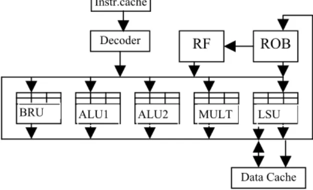
There are many possible superscalar organizations. Typically a superscalar organization consists of instruction fetch and branch prediction unit, decode and register renaming unit, instruction issue unit, execution unit, and commit unit. In this work we consider a most common organization of a superscalar processor which use distributed reservation station for each functional unit. The Re-order buffer (ROB) is used to commit the instructions. Figure 1 shows an organization of the DLX superscalar processor. For simplicity of presentation, we will use this particular organization to explain the various concepts. We believe, all the concepts can easily be generalized to other organizations.
Instr.cache
Decoder RF ROB
Figure 1 A Superscalar Organization of the DLX-SV Data Cache
BRU ALU1 ALU2 MULT LSU
We use an example superscalar DLX processor to demonstrate the concept. This processor uses a branch history table with 2 history bits to predict branch. It fetches four instructions and commits at most four instructions per cycle. Execution unit has 5 functional units (2 ALU, 1 Multiplier, 1 Branch unit, and 1 Load Store unit). Every unit has its own reservation station with 2 entries and ROB is implemented as a circular queue with 32 entries.
Superscalar Test Issues
Instruction based testing faces serious challenges due to the out of order execution with multiple functional units and in-order commit behavior, because it is the processor scheduler who decides the order of instruction execution, on the fly, and not the program that executes on the processor. This means that even if we have a test vector sequence generated under architectural constraints, when we apply such a sequence, there is no guarantee that the sequence will indeed be executed by the same functional unit for which it was meant to be. In fact, in a superscalar processor, the instructions in the sequence may be executed on a different functional unit and possibly in different order of instructions. Further, superscalar architecture uses buffers and queues, which makes it a challenging task to ensure that a given instruction resides at a given location in the buffer or queue with appropriate data at a given time. We explain this through the following example.
Example1: Consider a 4 instruction wide fetch superscalar implemented with 2 ALU, 1 Multiplier, 1 Shifter, 1 Load, 1 Store and 1 Branch Unit, where every unit has individual reservation station with 2 entries, and ROB has 32 entries. Processor instructions are represented as (I Rd, Rs1, Rs2) where I specifies operation, Rd is the destination, and Rs1 and Rs2 are the two source operands. Let a path through ALU be tested by an instruction sequence ADD followed by SUB. This path is from the reservation station to the reorder buffer. Let the desired operands be placed in the registers R2 and R3 for the ADD instruction and in registers R6 and R7 for the SUB instruction. Conventionally, we apply the test vectors in the following sequence:
I1: ADD R1, R2, R3 -- processor schedules this instr. to ALU1
I2: SUB R5, R6, R7 -- processor schedules this instr. to ALU2
The processor may schedule instructions I1 and I2
to two different ALUs. Therefore, this sequence will not apply the desired test to any of the ALUs. We will get the correct result in spite of having a faulty path, because the fault is not excited. A possible partial
solution to this problem is to concurrently test the two ALU’s by the following program segment.
I1: ADD R1, R2, R3 --processor schedules this instr. to ALU1
I2: ADD R21, R2, R3 -- processor schedules this instr. to ALU2
I3: SUB R5, R6, R7 -- processor schedules this instr. to ALU1
I4: SUB R25, R6, R7 -- processor schedules this instr. to ALU2
This can apply the test sequence to both the ALUs provided that these instructions are aligned, i.e., all these 4 instructions are fetched simultaneously. We can achieve this by having branch instruction preceding this set. Now, these instructions can be applied in our desired order. However, reservation station has two entries and first two instructions will be placed in the first entries of respective reservation stations and next two instructions will be placed in the second entries of the corresponding reservation stations. Therefore, the transition will not be launched and the path will remain untested. Again, a possible partial solution is to insert two instructions between I2 and I3 which are being scheduled to some other functional units. Therefore, the partial solution which can test the path from the first entry of reservation station to ROB is:
I1 J 2000H
I2: 2000H ADD R1, R2, R3 -- processor schedules it for -- ALU1 (stay at 1st position in RS)
I3 ADD R21, R2, R3 -- processor schedules it for -- ALU2 (stay at 1st position in RS)
I4: MULT R10, R11, R12 -- processor schedules it -- for Multiplier (Filler instr.) I5: SW R1, 100 (R15) -- processor schedules it for
-- Load store unit (Filler instruction)
I6: SUB R5, R6, R7-- processor schedules it for
-- ALU1 (stay at 1st position in RS)
I7: SUB R25, R6, R7-- processor schedules it for -- ALU2 (stay at 1st position in RS)
This way, we can make sure that the desired transitions will be created and propagated. Still the consideration to make sure that a result will be transferred to some particular entry of ROB is not looked at in this example. This simple example demonstrates the need for carefully developing a test sequence. The situation becomes even more complex when we consider feedback paths (due to the presence of forwarding logic) in the out of order execution engine.
Overview of Our Approach
In order to test the processor, we consider paths in datapath part and controller part separately. Clearly it is very difficult to separate out datapath and controller in superscalar processor as every stage carries data and control signals. We define data transfer activities between architectural registers, and data and address
part of pipeline registers, buffers and queues, as a part of the datapath. All other paths are considered as a part of the controller.
A graph theoretic model called Superscalar Instruction Execution graph (SIE-graph) has been developed that is constructed by using RT level description and instruction set architecture. This graph model is an extension of our pipeline instruction execution graph [15,16]. This graph models the complex superscalar behaviour. The paths in datapath are classified as functionally testable, functionally untestable, and potentially functionally testable. The graph is used to extract the constraints. Combinational constrained ATPG is used to generate test vectors for potentially functionally testable paths. Vectors thus generated can be applied in functional mode using carefully crafted instruction sequences generated under architectural constraints. The test vectors so generated are mapped to control signals and registers. Processor instructions are used as vehicles to deliver test patterns and collect test responses. It was indicated earlier that a superscalar processor executes instructions out-of program order using multiple functional units and it is the processor scheduler that decides, on the fly, which instruction will be executed by which functional unit. Therefore, we need to carefully craft the test instruction sequence that can force scheduler to execute in our desired order as well as on a given functional unit. We have developed a methodology to generate an instruction sequence for every path based on the graph that forces scheduler to execute instructions in our desired order. We limited ourselves to Non Robust testing of the path delay faults.
4. Superscalar Instruction Execution
Graph
The pipeline instruction execution graph (PIE- graph) presented in [14 ,15] is extended to capture the superscalar behaviour. SIE-graph is used for constraint extraction, path classification, and test instruction sequence generation.
SIE-graph can be constructed from RTL description and instruction set architecture. This includes the architectural registers, data and address part of the pipeline registers, buffers (Reservation Station), and queues (Re-Order Buffer). Note that this does not include control part of the registers, buffers, and queues.
Nodes of SIE graph are: (i) Architectural Registers
(ii) Part of architectural registers if it is independent readable and writtable
(iii) Equivalent register (Set of registers that behave identically with the instruction set, such as register file, and stacks)
(iv) Two special nodes, IN and OUT, which models the external world such as memory or IO devices (v) Data and address part of the pipeline registers (vi) Data and address part of buffers (like Reservation
Station)
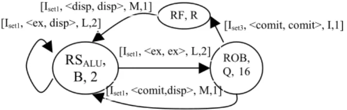
(vii) Data and address part of queues (like ROB) There are four types of nodes in SIE graph, which are special type (IN and OUT), register type (R), buffer type (B), and queue type (Q). Every node is labeled with its type and its attribute. The number of entries in buffers or queues are the attributes. Every node, except special node, is labeled with its name, node type, and the attributes of the type if any. For example, a node representing ROB with 16 entries is labeled as (ROB, Q, 16).
A directed edge between two nodes is drawn iff there exists at least one instruction responsible to transfer data (with or without manipulation) between corresponding two registers. Each edge is marked with a 4 –tuple [<instruction set>, <stage from, stage to>,
<logic type>, <cardinality>]. This 4 – tuple signifies that instructions from the <instruction set> are responsible for the transfer data from <stage from> to
<stage to> through the logic specified by <logic type>. Logic classification for logic type is based on our observation that many paths directly transfer data to the next stage using simple interconnects or through multiplexers. Keeping this in mind we classify logic in three types, namely interconnect (I), multiplexers (M), and processing logic (L). This classification simplifies the test generation process.
Superscalar processors often use multiple identical functional units. Edges for these are merged and a cardinality of the edge is specified as <cardinality>. SIE-graph for a part of the superscalar DLX processor is shown in the figure 2.
5. Tests for the Datapath
In this section we consider the paths that transfer the data between architectural registers, data and address part of the pipeline registers, buffers and
Figure 2 Part of SIE-graph of DLX-SV processor
RSALU, B, 2
ROB, Q,16 RF, R
[Iset1, <disp, disp>, M,1]
[Iset1, <ex, ex>, L,2]
[Iset1, <ex, disp>, L,2] [Iset3, <comit, comit>, I,1]
[Iset1, <comit,disp>, M,1]
queues. These paths are significant in number. Other paths are considered in the control section.
We assume that any instruction can follow any other instruction. Data forwarding takes place through the multiplexers. So, the data that can be received through forwarding path can also be received by the normal paths.
Path classification and constraint extraction: A path can be, i) functionally testable (FT) path, ii) functionally untestable (FUT) path, or iii) potentially functionally testable (PFT) path. In order to test a path, we extract the architectural constraints by using SIE- graph. There are two types of constraints, i) control constraints and ii) data constraints. Control constraints are the constraints on the control signals, which are responsible to transfer data between two nodes. These are obtained from the instructions marked on the corresponding edge on SIE-graph. Data constraints are the constraints on the justifiable data under the extracted control constraints. Data constraints are not applicable to Non Robust (NR) testable paths.
1. when logic type is interconnect ‘I’: These paths always carry data for the stages ahead. Therefore, these paths do not observe data constraints and can be tested as interconnects. These paths are classified as FT paths.
2. when logic type is multiplexer ‘M’: These paths pass through a set of multiplexers and behave as interconnects if control signals are properly assigned. Therefore these can also be tested as interconnects and classified as FT paths.
3. when logic type is processing logic ‘L’: These paths transfer data to destination node after manipulation.
(i) Normal paths:
These paths carry manipulated data inside the same pipeline stage. An instruction pair (IV1, IV2) is needed to test such a path. Any pair of instructions marked on the target path can be a test instruction, and can be used as IV1 and IV2. The constraints on the control signals of the modules in the target path are extracted under this set of instructions. Non Robust test do not observe any data constraints. For Robust test, we must consider the data constraints on the nodes which have out-edge to the target destination node inside the same stage and have some common instruction with the target edge. These paths are classified as PFT paths. (ii) Forwarding paths:
These paths carry data to the other stages. Therefore, they need a sequence of three instructions (IV1, IV2, and IV3) to test, where instruction IV1 and IV2 must be marked on the in-edge of the target source node, and IV3 must
be marked on the target edge. Non robust test do not observe any data constraints. These are also classified as PFT paths.
The forwarding paths from the ith entry of a buffer to the ith entry of the same buffer are classified as FUT paths because a transition cannot be launched and propagated through this path.
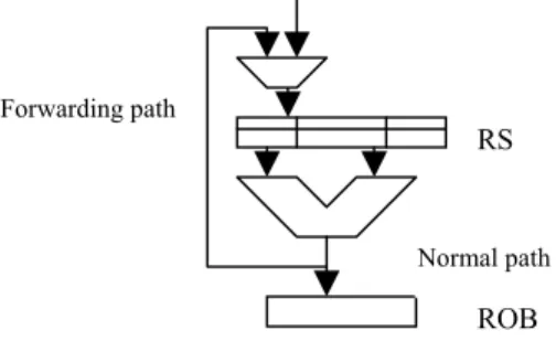
As shown in the fig. 3, the forwarding paths always go through MUX and the MUX can always be set to forward data. Therefore, the forwarding paths dominate the normal paths. Hence, it reduces the test generation effort.
Forwarding path
RS
Normal path ROB Figure 3 Forwarding and normal paths
Test Generation:
After extraction of constraints, constrained ATPG is used to generate the tests for the potentially functionally testable paths. The ATPG returns the test vectors for the functionally testable paths.
Test Instruction Sequence Generation:
The generated test vectors are mapped to the control signals and the registers. An instruction sequence is needed to apply the test vectors, justify the valus, and transfer the results to memory. We need to carefully craft an instruction sequence which can force scheduler to apply the test patterns in desired order. Test instruction generation procedures are explained through examples. In the examples we consider a processor that has 2 ALUs (1 ALU is considered for p
= 1 case to demonstrate some concepts), with 2-entry reservation station and 32 entry ROB. The fetch width of the processor is 4 instructions. The other functional units in the processor are multiplier, load store unit, and branch unit. We assume that the ADD instruction followed by the SUB instruction is a test instruction pair.
Paths from node Ni to No (register type nodes): Fetch and the decode stages usually consist of these paths. These stages are in-order processing stages. Let us consider that a test instruction sequence (IV1, IV2) is needed to test a path. Let the superscalar width be w, and the cardinality of the edge be p. The instruction
pair (IV1, IV2) can be applied by an instruction sequence [p number of I1 instructions, (w-p) other instructions except branching instructions, p number of I2
instructions].
Paths from a buffer type node Ni to queue type node No:
These paths originate from a reservation station and terminate at ROB. Let a reservation station has k entries and there be p number of identical functional units. The node representing the RS is labeled as (Ni, B, k). Let ROB be labeled with (No, Q, l). Derivation of test sequence for a path from ith entry of RS to jth entry of ROB is explained for two cases through examples. (i) when p = 1
Example 2: A path from 2nd entry in RS to 6th entry in ROB can be tested by the following instruction sequence. We assume that the processor has one ALU.
I1: J 2000H -- instruction for the alignment
I2: 2000H MULT R7, R8, R9 -- instr. for dependency
I3: AND R10, R7, R11--instr. to occupy 1st entry
I4: ADD R1, R2, R3 -- Instruction IV1
I5: SW R7, R13, R14 – Filler instruction
I6: SW R12, R15, R16 – Filler instruction
I7: SUB R4, R5, R6 – Instruction IV2
The first jump instruction flushes the RS and the ROB (assuming this entry is seen first time). The next 4 entries will be fetched in next cycle. The AND instruction (I3) will be placed at first entry of the RS and the ADD instruction (I4) will be placed in the second entry of the RS. During second cycle instruction I4 will be executed. Next four instructions will be fetched in the second cycle and instruction I7
will be placed in the second entry of the RS. During the third cycle, instruction I7 will be executed and will transfer the result to the 6th entry of the ROB. Hence, the path from the 2nd entry of RS to the 6th entry of ROB is tested.
In general, any path from the ith entry of a buffer (RS) to the jth entry of a queue (ROB) can be tested by an instruction sequence generated in the following way.
{Branch instruction, [(int(j/w)–1)*w] instructions at branch address which are not marked on the edge, instruction for dependency creation (should not be marked on the edge), (i-1) instructions marked from the instructions marked on the edge with dependency to the instructions which are not marked on the edge, IV1 instruction, (w-i-1) instructions which are not marked on the instruction, (rem (j-1/w)) instructions which are not marked the edge, IV2 instruction}. In case of 1<j<w, j = l+w. We
need a previously unseen branch instruction to align instructions and flush RS and ROB to make sure that desired data transfer takes place.
(ii) when p >1(Multiple identical functional units exist) In case of multiple identical units, our approach tests these units simultaneously. Here, we assume that p ≤ w, i.e., the number of multiple units is less than or equal to the fetch width. Let a test sequence (IV1, IV2) be required to test a path from the RS to the ROB.
Example 3: A path from 2nd entry in RS to 9th and 10th entries in ROB can be tested by the following instruction sequence.
I1: J 2000H -- instruction for the alignment
I2: 2000H LW R8, 100(R10)
I3: MULT R7, R8, R9 – for dependency creation
I4: AND R11,R7,R12 –
-- Schedule to 1st entry in RS of ALU1
I5: AND R13,R7,R14
-- Schedule to 1st entry in RS of ALU2
I6: ADD R1, R2, R3 – Instruction IV1
-- Schedule to 2nd entry in RS of ALU1
I7: ADD R21, R2, R3 --Instruction IV1
-- Schedule to 2nd entry in RS of ALU2
I8: SW R11, 100(R15) – Filler instruction
I9: SW R13, 104(R14) – Filler instruction
I10: SUB R24, R5, R6 – Instruction IV2
-- Schedule to 2nd entry in RS of ALU1 -- Transfer the result to the 9th entry of ROB
I11: SUB R4, R5, R6 – Instruction IV2
-- Schedule to 2nd entry in RS of ALU2 -- Transfer the result to the 10th entry of ROB
The procedure to test a path from any entry in a buffer to any entry in queue can be generalized without much difficulty.
Paths from a buffer type node Ni to buffer type node No (Forwarding paths):
These paths are responsible to forward data to the instructions residing in the RS without going through commit stage. These paths dominate the normal paths, i.e, a test for a forwarding path can also test the corresponding normal path. Hence, normal paths can be tested along with forwarding paths by using observation sequence for normal paths. An instruction sequence (Iv1, Iv2, Iv3) can test a path from RS (ith entry) to the same RS (jth entry) if it is applied in the following manner. This instruction sequence will test both normal paths and forwarding paths.
Example 4: A path from the 1st entry in RS to the 2nd entry in RS can be tested by the following instruction sequence.
I1: J 2000H -- instruction for the alignment
I2: 2000H ADD R1, R2, R3 -- Instruction IV1
I3: ADD R21, R2, R3 --
I4: SW R1, 100(R9)
I5: SW R21, 104(R14) – Filler instruction
I6: SUB R4, R5, R6 – Instruction IV2
I7: SUB R24, R5, R6 – Instruction IV2
I8: ORA R7, R4, R8 – Instruction IV3
I9: ORA R7, R24, R8 – Instruction IV3
Paths from a queue type node Ni to buffer type node No (From ROB to RS):
These are the paths which forward the data from the ROB to the RS. Following example explain the procedure to test a path from ith entry in ROB to jth entry in RS.
Example 5: A path from 3rd entry of ROB to 2nd entry in RS of multiplier unit can be tested by the following instruction sequence.
I1: J 2000H -- instruction for the alignment
I2: 2000H LW R1, 100(R10) I3: AND R11,R7,R12 –
I4: ADD R1, R2, R3 – Instruction IV1
-- Schedule to 3rd entry in ROB
I5: J 2100H
I6: 2100H LW R11, 100(R15) – Filler instruction
I7: AND R14, R12, R13
I8: SUB R4, R5, R6 – Instruction IV2
-- Schedule to 3rd entry in ROB
I9: SW R4, 104(R14) – Filler instruction
I10: MULT R7, R8, R9
-- Schedule to 1st entry in RS of multiplier
I11: MULT R10, R4, R11 – Instruction IV3
-- Schedule to 2nd entry in RS of Multiplier
The paths from ROB to register file can also be tested along with these paths by observing the result of Iv2.
6. Tests for the Controller
Instruction decoder dispatches the control signals with the data, which are used by the stages ahead. These control signals are often not structured. However they form a small group. We use this grouping to find the constraints. There are two types of constraints. i) intra group constraints, and ii) inter group constraints. . (i) Intra-group signal constraints: Some combinations of value on a small group of signals are not valid combination. Therefore, we need to extract all the legitimate values. For example, test control (test_ctrl) signals in DLX-SV are grouped in a group of 3 bits, and legitimate values are <0XX, 10X, and 110>.
(ii) Inter group signal constraints: We extract these constraints in terms of instructions, i.e., map to the instruction which can generate the particular combination and all possible combinations are extracted. For example, in DLX-SV when ALU ctrl (alu_ctrl) signal is 0000 the test control (test_ctrl) signal must be 000.
The part of a pipeline register, which carries the control signals is called control register. There are paths between control register (CR) to control register, control register to data register (DR), or data register (such as IR) to control register. The paths between CR- to-CR are used to carry the control signals for the pipeline stages ahead. These paths are connected directly and can be tested as interconnects. Paths from CR to DR are the paths which pass through the combinational logic such as paths from control register of RS to the ROB. Following example shows the procedure to test such paths.
Example 6: A path from 1st entry of CR in RS to 6th entry in ROB can be tested by the following instruction sequence.
I1: J 2000H -- instruction for the alignment
I2: 2000H ADD R1, R2, R3 -- Instruction IV1
I3: MULT R10, R11, R12
I4: SW R1, 100(R15)
I5: SW R10, 104(R15) – Filler instruction
I6: SUB R4, R5, R6 – Instruction IV2 I7: SUB R4, R5, R6 – Instruction IV2
Similarly, the test procedures for the paths from the control part of RS to the data part of RS (feed back paths) and other paths can also be developed as explained in the previous section.
7. Conclusion
This paper highlighted the issues that are pertinent to testing superscalar architecture in the functional mode of operation. A graph theoretic model is developed to extract the constraints. We have developed the test procedures that can force the processor scheduler to execute program in our desired order. Hence, these procedures can apply test vectors in the functional mode of operation. Superscalar DLX processor (DLX-SV) is implemented and it will be used as a vehicle to verify the methods described in this paper.
Acknowledgement
This work was supported in part by Semiconductor Technology Academic Research Center (STARC) under the Research Project and in part by Japan Society
for the Promotion of Science (JSPS) under Grants-in- Aid for Scientific Research B (2) (No. 15300018) and the grant of JSPS Research Fellowship (No. L04509).
References:
[1] S.M. Thatte and J. Abraham, “Test generation for Microprocessors”, IEEE Trans. on Computers, Vol. C- 29, No. 6, June 1980, pp. 429-441.
[2] J. Shen and J.A. Abraham, “Native Mode Functional Test Generation for Processors with Applications to Self-Test and Design Validation”, Proc. of the International Test Conference 1998, pp. 990-999.
[3] K. Batcher and C. Papachristou, “Instruction Randomization Self Test for Processor Cores” Proc. of the VLSI Test Symposium 1999, pp. 34-40.
[4] L. Chen, and S. Dey, “Software-Based Self-Testing Methodology for Processor Cores”, IEEE Trans. on CAD of Integrated Circuits and Systems, Vol. 20, No.3, March 2001, pp. 369-380.
[5] N. Krantis, A. Paschalis, D. Gizopoulos, and Y. Zorian,
“Instruction-Based Self-Testing of Processor Cores”, Journal of Electronic Testing: Theory and Application (JETTA) 19, 2003, pp 103-112.
[6] K.Kambe, M.Inoue, and H. Fujiwara, “Efficient Template Generation for Instruction-Based Self-Test of Processor Cores”, Proc. of Asian Test Symposium, 2004, pp. 152- 157.
[7] L. Chen, S. Ravi, A. Raghunath, and S. Dey, “A Scalable Software-Based Self-Test Methodology for Programmable Processors”, Proc. of Design Automation Conference 2003, pp. 548-553.
[8] N.Krantis, G.Xenoulis, A.Paschalis, D.Gizopolous, and Y.Zorian, “Application and Analysis of RT-Level Software-Based Self-Testing for Embedded Processor Cores”, Proc. of International Test Conference, 2003, pp 431-440.
[9] A. Paschalis, and D. Gizopoulos, “ Effective Software- Based Self-Test Strategies for On-Line periodic Testing of Embedded Processors”, Proc. of Design and Test in Europe 2004, pp 578-583.
[10] W.-C. Lai, A. Krstic, and K.-T. Cheng, “On Testing the Path Delay Faults of a Microprocessor Using its Instruction Set”, Proc. of the VLSI Test Symposium 2000, pp. 15-20.
[11] W.-C. Lai, A. Krstic, and K.-T. Cheng, “Test Program Synthesis for Path Delay Faults in Microprocessor Cores”, Proc. of International Test Conference 2000, pp 1080-1089.
[12] W.-C. Lai, and K.-T. Cheng, “Instruction-Level DFT for Testing Processor and IP Cores in System-on-a-Chip”, Proc. of the Design Automation Conference 2001, ACM Press, NY, 2001, pp. 59-64.
[13] V. Singh, M. Inoue, K.K. Saluja, and H. Fujiwara,
“Instruction-Based Delay Fault Testing of Processor Cores”, Proc. of the International Conference on VLSI Design 2004, pp 933-938.
[14] V. Singh, M. Inoue, K.K. Saluja, and H. Fujiwara,
“Delay Fault Testing of Processor Cores in Functional Mode”, IEICE Trans. on Information & Systems, Vol. E-88D, No. 3, March 2005, pp. 1-9.
[15] V. Singh, M. Inoue, K.K. Saluja, and H. Fujiwara,
“Instruction-Based Delay Fault Self-Testing of Pipelined Processor Cores”, Proc. of International Symposium on Circuits and Systems 2005. To appear
[16] V.Singh, M.Inoue, K.K.Saluja, and H.Fujiwara,
“Software-Based Delay Fault Self-Testing of Pipelined Processor Cores”, NAIST Technical report. No. 2004006 Sept. 2004.
http://isw3.aist-nara.ac.jp/IS/TechReport/2004006 [17] A. Krstic and K.-T. Cheng, Delay fault testing for VLSI
circuits, Kluwer Academic Publishers, 1998.