Efficient Path Delay Test Generation Based on
Stuck-at Test Generation Using Checker Circuitry
Tsuyoshi Iwagaki , Satoshi Ohtake , Mineo Kaneko and Hideo Fujiwara School of Information Science, Japan Advanced Institute of Science and Technology (JAIST)
1-1 Asahidai, Nomi, Ishikawa 923-1292, Japan E-mail: iwagaki, mkaneko @jaist.ac.jp
Graduate School of Information Science, Nara Institute of Science and Technology (NAIST) Kansai Science City 630-0192, Japan
E-mail: ohtake, fujiwara @is.naist.jp
Abstract— This paper proposes an approach to non-robust and functionally sensitizable path delay test generation through stuck- at test generation. In this approach, to generate two-pattern tests for path delay faults in a combinational circuit, checker circuitry is constructed which is composed of logic gates corresponding to the mandatory assignments for detecting the faults. This checker circuitry allows us to use any existing combinational stuck-at test generation tool. Since today’s stuck-at test generation tools reach a mature level, the proposed approach can efficiently solve the path delay test generation problem for combinational circuits. Experimental results show that the approach can speed up path delay test generation and can improve fault efficiency. This paper also discusses how a scan circuit and the issues of over-testing and test power are handled in the proposed test generation framework.
I. INTRODUCTION
Testing of path delay faults (PDFs) as well as stuck-at faults (SAFs) is an essential task for today’s high speed circuits. Automatic test pattern generation (ATPG) techniques for SAFs have been well-studied over the decades, and those techniques for combinational circuits have reached a mature level. For PDFs, some efficient techniques have also been in- vestigated [1]–[4]. These techniques adopted new multi-valued logic systems for detecting PDFs in a combinational circuit, and considered algorithms adapted to the logic systems. In this way, on the one hand, there have been methods using new multi-valued logic systems. But, on the other hand, there have been methods using existing ATPG techniques for SAFs to handle PDFs [5]–[8]. All of the methods of [5]–[8] is based on a test generation framework using a modified circuit. In this framework, to generate two-pattern tests for PDFs in a combinational circuit, the circuit is first transformed into a different one only during test generation. Then, a stuck- at test generation algorithm is applied to the corresponding SAFs in the transformed circuit. The generated test patterns for the corresponding SAFs are finally transformed into the two-pattern tests for the original PDFs. This framework can efficiently solve the problem of path delay test generation for a combinational circuit by using a mature ATPG tool for SAFs. Our work is also based on this framework. Next, we review each of the above related works further.
Which class of PDFs to be targeted and the circuit size after transformation are main concerns in the above test generation framework. A modified circuit based on a leaf-dag, in which a fanout and an inverter are only permitted at the primary inputs and the output of an inverter is not allowed to have a fanout, is used in [5]. The circuit size depends on the number of PDFs targeted. Although this method can efficiently handle the problem of path delay test generation for a combinational circuit, only robust PDFs [9] are targeted. There has been a method to handle larger classes of PDFs: singly-testable (ST) and multiply-testable (MT) PDFs [6]. Since this method can handle ST and MT PDFs, a large part of delay defects can be covered compared to [5]. However, this method is not applicable to large circuits because the size of the modified circuit used in the method depends on the total number of paths in a given combinational circuit. Recently, two methods to overcome the disadvantages of [5] and [6] have been proposed in [7] and [8]. Both methods are capable of handling non- robust (NR) PDFs [9], and the size of the modified circuits used in the methods depends on the number of PDFs targeted rather than the total number of paths in a given combinational circuit. Although, indeed, the disadvantages of [5] and [6] are alleviated in [7] and [8], other testable classes of PDFs such as functionally sensitizable (FS) [9] PDFs are not handled yet. This paper presents a test generation method for NR and FS PDFs in a combinational circuit. In the proposed method, to generate two-pattern tests for PDFs in a combinational circuit, checker circuitry is constructed which is composed of logic gates corresponding to the mandatory assignments for detecting the faults. Like the other approaches of [5]–[8], this checker circuitry allows us to use any existing combinational stuck-at test generation tool. The size of the modified circuit used in our method depends on the number of PDFs targeted during test generation. This feature enables us to handle a large circuit in which the total number of paths is usually very large. Furthermore, our method can handle a large class of PDFs, i.e., FS PDFs, compared with [7] and [8]. Through experimental results, we show that our method can accelerate path delay test generation and can improve fault efficiency
IEEE/ACM International Conference on Computer-Aided Design (ICCAD'07), pp. 418-423, Nov. 2007.
TABLE I
OFF-INPUT CONDITIONS FOR DETECTION
On-input Off-input conditions
transitions NR FS
cv ncv ncv
ncv cv ncv ncvncvcvor
compared with an ordinary method. In this paper, we also discuss some applications of our method to deal with the over- testing and test power problems.
II. PRELIMINARIES
This paper targets non-robust (NR) and functionally sensiti- zable (FS) path delay faults (PDFs) in a combinational circuit. Some definitions and notations are described below.
In a combinational circuit , a path is defined as a sequence of gates. The starting (resp. ending) point of corresponds to a primary input (resp. primary output) of . There exist two types of PDFs on depending on the direction of the transition at the starting point of , i.e., rising and falling PDFs. A controlling value, which is denoted as cv, of a gate is a value at an input of the gate that determines the value of the gate output regardless the values of the other inputs. A non-controlling value, which is denoted as ncv, of a gate is the complement value of its controlling value. A gate input is referred to as an on-input of if it is on . A gate input is referred to as an off-input of if it is an input to a gate on but it is not an on-input. Whether a PDF is NR or FS is determined according to whether the mandatory values can be assigned to all the off-inputs. Table I lists the off-input conditions for NR PDFs and FS PDFs, where is an unknown value. In notation , (resp. ) represents the first vector (resp. second vector) of a vector pair on a gate input.
III. PROPOSEDTESTGENERATIONFRAMEWORK This section discusses a test generation framework for NR and FS PDFs using checker circuitry. First, we present a test generation model based on checker circuitry. Then, we propose a test generation procedure using the model, and prove the correctness of the proposed method.
A. Test Generation Model
Given a combinational circuit and a set of PDFs in , a test generation model TGMfor (PDTGM) is constructed as follows.
(1) Duplicate as and .
(2) Insert additional signal lines into all the starting points of the paths corresponding to in and .
(3) Insert additional signal lines into all the off-inputs of the gates on the paths in and .
(4) Create a checker circuit C according to the transitions at the starting points and the off-input conditions.
Checker Circuit
Mask Circuit
stuck-at fault f’ C
CMf CCf
(a) Original circuit: C path delay fault f
C
C2 1
(b) PDTGM for f: CTGMf
Fig. 1. Overview of a test generation model for PDFs (PDTGM)
(5) Create a mask circuit M.
(6) Connect all the additional signal lines to C, and connect the outputs of C and the ending points of the paths in
to M.
Figure 1 shows the overview of a PDTGM for one PDF . In this figure, and are used to generate the first vector and the second vector of two-pattern tests, respectively. The checker circuit in this figure outputs ‘1’ only if the condition for the primary on-input and all the off-input conditions are satisfied. PDF in the original circuit corresponds to the stuck-at fault (SAF) on the bottom input of the mask circuit. The mask circuit blocks the fault effect of except when the checker circuit outputs ‘1.’ If is a rising (resp. falling) PDF and the number of inverters on the path with is even, is a stuck-at 0 (resp. 1) fault. In contrast, if is a rising (resp. falling) PDF and the number of inverters on the path with is odd, is a stuck-at 1 (resp. 0) fault. In (4) (resp. (5)) of the above procedure, C (resp. M) includes sub checker circuits (resp. mask circuits) and has outputs, where denotes the number of PDFs in . In other words, in Figure 1,
pairs of a sub checker circuit and a sub mask circuit must exist in parallel. If NR PDFs (resp. FS PDFs) are targeted, the conditions of “NR” (resp. “FS”) shown in Table I are used
a b
c d e
f g
h
i
Fig. 2. Example circuit
to create checker circuitry. A PDTGM for NR PDFs (resp. FS PDFs) is hereinafter referred to as an NR-TGM (resp. FS- TGM).
For a PDF in a combinational circuit , the size of the NR-TGM (resp. FS-TGM) obtained by the above procedure is
roughly approximated as (resp. )
[gates], where is the number of gates in , and is the number of gates on the path corresponding to . Here, it is assumed that all the circuits of our test generation model are composed of 2-input gates.
B. Test Generation Procedure
Given a combinational circuit and a set of PDFs in , test generation is performed as follows.
(1) Transform into a PDTGM TGM.
(2) For each , where is the set of SAFs corre- sponding to , perform the following steps.
(a) Generate a test pattern for by performing stuck-at test generation on TGM.
(b) Perform fault simulation by applying the test pattern to TGM, then the SAFs detected by it are dropped from .
(c) Repeat step (2) until is empty.
(3) Transform the obtained test patterns for into the two- pattern tests for .
Note that, in (1) of the above procedure, TGMis an NR- TGM (resp. FS-TGM) if NR PDFs (resp. FS PDFs) are targeted.
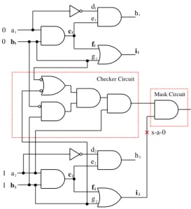
To clarify our test generation method, we give an example here. Let us consider performing test generation for FS PDFs in the example circuit shown in Figure 2. Figure 3 is a FS- TGM for the rising PDF on path (b, c, f, i) in the example circuit. By performing stuck-at test generation on the FS- TGM, for example, a two pattern test (a, b) = ( , ) is obtained.
The correctness of our method is guaranteed by the follow- ing theorem.
Theorem 1: Let and be a combinational circuit and a PDF in the circuit, respectively. Let NR-TGM(resp. FS-TGM) and be an NR-TGM (resp. FS-TGM) for and the SAF
a b
c d e
f g
h
i
a b
c d e
f g
h
i Checker Circuit
Mask Circuit
s-a-0
1
1
1
1 1 1
1
1
1
2
2
2
2
2
2 2
2 2
0 0
1 1
Fig. 3. FS-TGM for the rising PDF on path (b, c, f, i)
corresponding to , respectively. Then, is NR (resp. FS) if and only if is testable.
Proof: First, we show that if is testable, is NR (resp. FS). Since is testable, there exists a test pattern . Let be the two-pattern test for mapped from . Clearly, if is applied to , it is guaranteed that the appropriate transition is launched at the starting point of the path with and all the off-inputs satisfy the conditions for the detectability of an NR PDF (resp. FS PDF) by the checker circuit. This implies that
is NR (resp. FS).
Next, we demonstrate that if is NR (resp. FS), is testable. Since is NR (resp. FS), there exists a two-pattern test . Let be a test pattern for NR-TGM (resp.
FS-TGM) in which the pattern for the first copy of is mapped from , and that for the second copy of is mapped from . By applying to NR-TGM (resp. FS-TGM), the checker circuit produces the value that makes the mask circuit inactive. This is because the structures of and are identical to the structure of , and sets all the off- inputs of to the values that satisfy the conditions for the detectability of an NR-PDF (resp. FS-PDF). Moreover, is activated by . Since the mask circuit is inactive, the fault effect of is propagated to a primary output. Hence, is testable and the proof is complete.
Theorem 1 implies that is not FS, i.e., functional unsen- sitizable, if is untestable in an FS-TGM. Any functional unsensitizable PDF never impacts the timing behavior of a circuit [9]. Thus, our method can also identify false paths in a combinational circuit.
IV. EXPERIMENTALRESULTS
To show the feasibility of our method and its effective- ness, we conducted the following experiments on a Linux
TABLE II
CIRCUIT SIZES AND TIME FOR CONSTRUCTION
Circuit Class ORG-size[gates] TGM-size[gates] TRN-time [s] c5315 NRFS 2,309 129,17723,048 3.094,44 c6288 NRFS 2,416 646,73292,309 19.8723.04 c7552 NRFS 3,512 136,12224,099 4.455.08 s5378 NRFS 3,137 23,40983,069 3.193.51 s6669 NRFS 3,558 250,83624,000 7.988.37 s9234.1 NRFS 6,019 124,36136,051 4.705.18 s13207.1 NRFS 9,227 29,87075,208 3.213.51 s15850.1 NRFS 10,840 150,92138,702 6.627.11 s35932 NRFS 19,526 161,50554,088 5.735.89 s38417 NRFS 25,451 172,16844,806 6.577.06 s38584.1 NRFS 22,107 116,00133,799 5.205.58
TABLE III
TEST GENERATION RESULTS FORNRANDFS PDFS
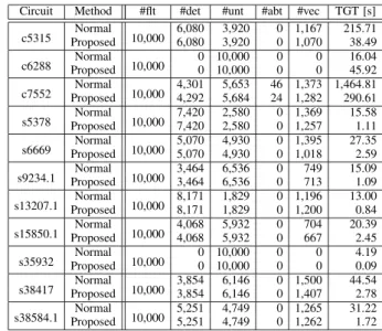
Circuit Class #flt #det #unt #abt #vec TGT [s] c5315 NRFS 10,000 6,0807,442 3,9202,558 00 1,0701,065 38.4937.06 c6288 NRFS 10,000 00 10,00010,000 00 00 137.2145.92 c7552 NRFS 10,000 4,2926,949 5,6843,043 248 1,2821,868 290.61256.80 s5378 NRFS 10,000 7,4208,702 2,5801,298 00 1,257932 1.111.58 s6669 NRFS 10,000 5,0705,090 4,9304,910 00 1,018819 12.542.59 s9234.1 NRFS 10,000 3,4644,778 6,5365,222 00 713668 1.092.66 s13207.1 NRFS 10,000 8,1718,920 1,8291,080 00 1,200801 0.841.02 s15850.1 NRFS 10,000 4,0685,729 5,9324,271 00 667690 2.458.39 s35932 NRFS 10,000 1310 10,0009,869 00 200 0.090.61 s38417 NRFS 10,000 3,8546,082 6,1463,918 00 1,4071,460 2.785.43 s38584.1 NRFS 10,000 5,2517,088 4,7492,912 00 1,2621,529 1.724.77
workstation (CPU: Opteron 150 2.4GHz, Memory: 8GB). In the experiments, we used large ISCAS 85’ benchmark circuits (c5315, c6288 and c7552) and the combinational parts of large ISCAS ’89 benchmark circuits (s5378, s6669, s9234.1, s13207.1, s15850.1, s35932, s38417 and s38584.1). For each circuit, we extracted long paths by using a commercial static timing analyzer, and we used a commercial ATPG tool which can handle both SAFs and PDFs.
First, to show the feasibility of the proposed method, we classified the PDFs on the long paths into NR or FS PDFs by using our method. In each circuit, we constructed
TABLE IV
NORMAL APPROACH VS.OUR APPROACH
Circuit Method #flt #det #unt #abt #vec TGT [s] c5315 ProposedNormal 10,000 6,0806,080 3,9203,920 00 1,1671,070 215.7138.49 c6288 ProposedNormal 10,000 00 10,00010,000 00 00 16.0445.92 c7552 ProposedNormal 10,000 4,3014,292 5,6535,684 4624 1,3731,282 1,464.81290.61 s5378 ProposedNormal 10,000 7,4207,420 2,5802,580 00 1,3691,257 15.581.11 s6669 ProposedNormal 10,000 5,0705,070 4,9304,930 00 1,3951,018 27.352.59 s9234.1 ProposedNormal 10,000 3,4643,464 6,5366,536 00 749713 15.091.09 s13207.1 ProposedNormal 10,000 8,1718,171 1,8291,829 00 1,1961,200 13.000.84 s15850.1 ProposedNormal 10,000 4,0684,068 5,9325,932 00 704667 20.392.45 s35932 ProposedNormal 10,000 00 10,00010,000 00 00 4.190.09 s38417 ProposedNormal 10,000 3,8543,854 6,1466,146 00 1,5001,407 44.542.78 s38584.1 ProposedNormal 10,000 5,2515,251 4,7494,749 00 1,2651,262 31.221.72
the PDTGMs for NR and FS PDFs by using an in-house Perl program. Table II shows the sizes of each circuit (“ORG- size”) and its PDTGM (“TGM-size”) for NR or FS PDFs, which are estimated by the ATPG tool, and time required for constructing a PDTGM (“TRN-time”). Note that the ATPG tool removed some unnecessary gates during test generation. Rows “NR” and “FS” represent the results of test generation for NR and FS PDFs, respectively. In all the circuits, the sizes of the PDTGMs became large, especially in “FS,” compared with those of the original circuits. However, this is not critical for the efficiency of test generation as demonstrated later. Even if increasing the size of a PDTGM is critical for some aspects such as the memory size used during test generation, it can be alleviated as follows. In the checker circuit of a PDTGM, only its functionality is important. Therefore we can perform logic minimization for the checker circuit, and it will produce a much simpler circuit. The checker circuit, moreover, can be reduced by targeting a reasonable number of faults at a time and by performing test generation several times. In Table III, columns “#flt,” “#det,” “#unt” and “#abt” give the number of targeted faults, detected faults, untestable faults identified during test generation for NR or FS PDFs and aborted faults, respectively. Columns “#vec” and “TGT” denote the number of two-pattern tests and test generation time including fault simulation time, respectively. Theoretically, all the NR PDFs are also FS. In Table III, the number of FS PDFs was always larger than that of NR PDFs. Some non-robustly untestable PDFs are FS in theory. This can also be observed in Table III. For example, in the case of c5315, 1,362 of 3,920 non-robustly untestable PDFs were FS. The remaining 2,558 PDFs were functionally unsensitizable which do not affect the circuit performance.
TABLE V
MULTI-PASS TEST GENERATION
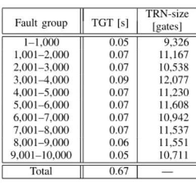
Fault group TGT [s] TRN-size[gates]
1–1,000 0.05 9,326
1,001–2,000 0.07 11,167 2,001–3,000 0.07 10,538 3,001–4,000 0.09 12,077 4,001–5,000 0.07 11,230 5,001–6,000 0.07 11,608 6,001–7,000 0.07 10,942 7,001–8,000 0.07 11,537 8,001–9,000 0.06 11,551 9,001–10,000 0.05 10,711
Total 0.67 —
Here, we show the experimental results to verify the ef- fectiveness of our method. The best way to verify the effec- tiveness of our method is that the results obtained by using the following two approaches are compared. One approach uses the most efficient ATPG tool for PDFs, and the other approach uses the proposed method with the most efficient ATPG tool for SAFs. However, it is difficult to perform such a experiment. Instead, we performed the following experiment. Since the commercial ATPG tool that we used can handle not only SAFs but also PDFs in a combinational circuit, we compared a normal method (“Normal”) where the tool targets PDFs to our method (“Proposed”) where the tool targets SAFs. Note that since the ATPG tool cannot handle FS PDFs, NR PDFs were only targeted in this experiment. Table IV shows the test generation results of “Normal” and “Proposed.” Except the case of c6288, we achieved short test generation time compared with the normal method. Furthermore, in the case of c7552, our method reduced the number of aborted faults. In terms of the number of two-pattern tests, our method also obtained good results. To examine the case of c6288 further, an additional experiment was performed. In the additional experiment, 10,000 PDFs were partitioned into 10 groups. Each group has 1,000 PDFs. Our method was applied to each group, i.e., test generation was performed 10 times. The total time required for constructing 10 PDTGMs was 20.65 seconds. As shown in Table V, the total test generation time was drastically improved from 45.92 seconds to 0.67 seconds. In this way, the efficiency of our method can be enhanced. In future work, we should consider a good way to partition given PDFs into groups in order to enhance the efficiency of our method.
From the above experimental results, we can see that our test generation framework using checker circuitry is effective and can easily be implemented by making use of an existing ATPG tool for SAFs.
V. SOME APPLICATIONS
This section briefly discusses some applications of the proposed test generation framework using checker circuitry. In the future, the following topics should be discussed in detail.
Checker Circuit for the Number of Transitions and/or
Checker Circuit for Invalid States PDTGM for a Scan Circuit
To the mask circuit From circuit nodes
Fig. 5. Test generation model considering over-testing and/or test power for a scan circuit
A. Scan Circuits
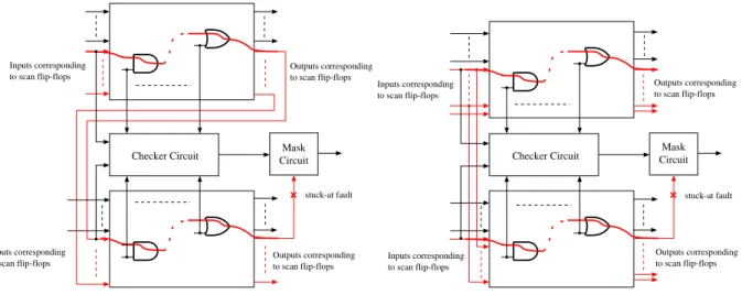
In section III, a combinational circuit is targeted. Let us consider a scan circuit here. Scan methodology for PDFs can be classified into two categories: the enhanced scan method [10] and the standard scan one. The standard scan method can be further divided into the broadside method [11] and the skewed-load method [12]. For a circuit designed by the enhanced scan method, our method described in section III can be applied without modification. In the case of the standard scan method, PDTGMs can be represented as Figure 4. Fig- ure 4(a) explains how to generate broadside tests for PDFs. The combinational part of a scan circuit is duplicated and connected as Figure 4(a), that is, the outputs corresponding to the scan flip-flops (FFs) in the first copy are cascaded to the inputs corresponding to the scan FFs in the second copy. In the case of skewed-load testing shown in Figure 4(b), the respective inputs corresponding to the scan FFs in the first copy are connected to the inputs corresponding to those adjacent scan FFs on the scan chain. By using the above test generation model, we can test PDFs in a scan circuit. B. Over-testing and Test Power
Over-testing [14] and excessive test power [15] in scan methodology are crucial issues, and it is important to enhance the test quality and to reduce the yield loss caused by those issues. Let us consider here how to deal with such problems under the proposed framework.
For a scan circuit, detecting PDFs by unsettable values in the scan FFs during normal operation is one of the main reasons that over-testing is induced. To avoid this phenomenon, the information of invalid states in a given circuit should be taken into account during test generation. In our test generation method, by checking the information of invalid states, which are extracted by some method such as [13], as well as the conditions of the off-inputs, over-testing can be alleviated.
Excessive test power may not only damage the circuit under test, but may also cause instantaneous voltage drops which result in making the test invalid. In testing of static faults such as SAFs, this undesirable situation can be avoided by slowing down the clock frequency during testing. We cannot, however,
(a) PDTGM for broadside testing (b) PDTGM for skewed-load testing Checker Circuit CircuitMask
stuck-at fault Inputs corresponding
to scan flip-flops
Outputs corresponding to scan flip-flops
Outputs corresponding to scan flip-flops
Inputs corresponding to scan flip-flops
Checker Circuit CircuitMask
stuck-at fault
Outputs corresponding to scan flip-flops Inputs corresponding
to scan flip-flops
Inputs corresponding to scan flip-flops
Outputs corresponding to scan flip-flops
Fig. 4. PDTGMs for a scan circuit
slow down the frequency in delay testing. In this case, power- aware two-pattern tests are required, i.e., we should test delay faults under power constraints in a scan environment. Such constraints may be estimated by applying functional patterns to the circuit. As shown in Figure 4, the first and second vectors of two-pattern tests are considered separately. This makes it possible to identify which circuit nodes have transitions. As a result, we can compare the number of transitions in a given circuit to the information of power constraints during test generation. This can be realized by some kind of checker circuitry in our framework.
It can be seen from the above discussion that our test generation framework can consider various properties in a unified test generation model of Figure 5.
VI. CONCLUSIONS
In this paper, we presented a test generation framework for PDFs using checker circuitry. This framework can utilize existing mature ATPG techniques for SAFs. Since our method can handle FS PDFs, false paths in a combinational circuit can be identified. We showed that our method is effective in terms of test generation time, fault efficiency and the number of two-pattern tests through the ISCAS ’85 and ’89 benchmark circuits. The feasibility of applying our framework to the over- testing and test power problems was also discussed.
ACKNOWLEDGMENTS
This work was supported in part by the Research Promoting Expenses for Associates of JAIST, the Foundation for the Promotion of Industrial Science, and the Japan Society for the Promotion of Science under Grants-in-Aid for Young Scien- tists (B) (No. 17700062) and for Scientific Research (C) (No. 19560340).
REFERENCES
[1] G. L. Smith, “Model for delay faults based upon paths,” Int. Test Conf., pp. 342–349, 1985.
[2] C. J. Lin and S. M. Reddy, “On delay fault testing in logic circuits,” IEEE Trans. on CAD, Vol. CAD-6, No. 5, pp. 694–703, Sep. 1987. [3] S. Patil and S. M. Reddy, “A test generation system for path delay
faults,” Proc. Int. Conf. on Comp. Design, pp. 40–43, 1989. [4] K. Fuchs, F. Fink and M. H. Schulz, “DYNAMITE: an efficient
automatic test pattern generation system for path delay faults,” IEEE Trans. on CAD, Vol. 10, No. 9, pp. 1323–1335, Oct. 1991.
[5] A. Saldanha, R. K. Brayton and A. L. Sangiovanni-Vincentelli, “Equiv- alence of robust delay-fault and single stuck-fault test generation,” Proc. Design Automation Conference, pp. 173–176, 1992.
[6] M. A. Gharaybeh, M. L. Bushnell and V. D. Agrawal, “Classification and Test Generation for path-delay faults using single stuck-at fault tests,” Journal of Electronic Testing: Theory and Application, Vol. 11, No. 1, pp. 55–67, Aug. 1997.
[7] S. Ohtake, K. Ohtani and H. Fujiwara, “A method of test generation for path delay faults using stuck-at fault test generation algorithms,” Proc. Design, Automation and Test in Europe, pp. 310–315, 2003. [8] D. Xiang, K. Li, H. Fujiwara and J. Sun, “Generating compact robust
and non-robust tests for complete coverage of path delay faults based on stuck-at tests,” Proc. 24th IEEE International Conference on Computer Design, pp. 446–451, 2006.
[9] A. Krstic and K.-T. Cheng, Delay fault testing for VLSI circuits, Kluwer Academic Publishers, 1998.
[10] B. I. Dervisoglu and G. E. Stong, “Design for testability: using scanpath techniques for path-delay test and measurement,” Proc. International Test Conference, pp. 365–374, 1991.
[11] J. Savir and S. Patil, “Broad-side delay test,” IEEE Trans. on CAD, Vol. 13, No. 8, pp. 1057–1064, Aug. 1994.
[12] J. Savir and S. Patil, “Scan-based transition test,” IEEE Trans. on CAD, Vol. 12, No. 8, pp. 1232–1241, Aug. 1993.
[13] H. C. Liang, C. L. Lee and J. E. Chen, “Invalid state identification for sequential circuit test generation,” Proc. Asian Test Symposium, pp. 10– 15, 1996.
[14] International technology roadmap for semiconductors, http://public.itrs.net/, 2005.
[15] P. Girard, “Survey of low-power testing of VLSI circuits,” IEEE Design and Test of Computers, Vol. 19, No. 3, pp. 82–92, May 2002.