Effects of Impurity Doping at ppm Level in
Organic Semiconductors
OHASHI CHIKA
Doctor of Philosophy
Department of Functional Molecular Science
School of Physical Sciences
SOKENDAI (The Graduate University for
Advanced Studies)
定
Effects of Impurity Doping at ppm Level
in Organic Semiconductors
Chika Ohashi
SOKENDAI (The Graduate University for Advanced Studies)
School of Physical Sciences
Dept. of Functional Molecular Science
Preface
The author carried out the experiments and wrote the doctoral thesis under the guidance of Professor Masahiro Hiramoto at Department of Functional Molecular Science, School of Physical Sciences, SOKENDAI. This thesis indicates the effects of impurity doping at ppm level in organic semiconductors.
The author believes that the work described in this thesis will lead to the clarification of detailed doping mechanism and the new types of organic device using doped organic single crystals.
Chika Ohashi
Dept. of Functional Molecular Science School of Physical Sciences
SOKENDAI
10th January 2017
Contents
Chapter 1: General Introduction 1
1.1. Background to Inorganic Semiconductors 1
1.2. Introduction to Organic Semiconductors 3
1.2.1 History 3
1.2.2 Materials 4
1.2.2.1 Organic Semiconductors 4
1.2.2.2 Dopants 6
1.3. Impurity Doping for Organic Semiconductor 7
1.3.1 Control of Carrier Concentration 7
1.3.2 Mechanism of Impurity Doping 8
1.3.3 Doped Organic Photovoltaic Cells 11
1.4. Measurement Techniques for Doped Organic Semiconductors 13
1.4.1. Energy Band Mapping 13
1.4.2. Hall effect Measurements 15
1.4.3. Organic Field-Effect Transistors 17
1.4.4. Organic Photovoltaic Cells 19
1.5. Motivation for This Doctoral Thesis 21
1.6. Overview for This Doctoral Thesis 22
1.7. References 25
Chapter 2: Experimental Equipment and Methods 29
2.1. Purification of Organic Semiconductors 29
2.2. Extremely Low Concentration Doping for Organic Semiconductors 31
2.3. Measurements of Doped Organic Semiconductors 34
2.3.1. Hall effect Measurements 34
2.3.2. Kelvin Probe Measurements 36
2.3.3. Organic Field-Effect Transistors 38
2.3.4. Organic Photovoltaic Cells 39
2.3.5. Thin-film Structures 42
2.4. References 44
Chapter 3: Hall effects for Doped Organic Single Crystals 46
3.1. Introduction 47
3.2. Experimental 49
3.2.1. Homoepitaxial Cells 49
3.2.2. Hall effect Measurements 50
3.2.3. Single Crystal Doping 51
3.3. Results and Discussion 52
3.3.1. Doped Homoepitaxial Layer 52
3.3.2. Hall Signal 54
3.3.3. Hole Concentration and Hall Mobility 59
3.3.4. AFM and GIXD for Doped Single Crystals 62
3.3.5. Contact Size Effect 65
3.3.6 Doped Amorphous Films 68
3.4. Conclusion 70
3.5. References 71
Chapter 4: Field-Effect Mobility of Doped Organic Single Crystals 74
4.1. Introduction 75
4.2. Experimental 76
4.3. Results and Discussion 78
4.3.1. FET Characteristics 78
4.3.2. Activation Energy of Hole Traps 80
4.3.3. Concentration of Hole Traps 83
4.4. Conclusion 88
4.5. References 89
Chapter 5: Effects of Impurity Doping in Simple n+p-Homojunction Organic Photovoltaic Cells
91
5.1. Introduction 92
5.2. Experimental 93
5.3. Results and Discussion 95
5.3.1. Formation of n+p-homojunction 95
5.3.2. Photovoltaic Characteristics 97
5.3.3. Energy Structures 99
5.3.4. Doping Concentration Dependence of Photovoltaic Characteristics 102
5.4. Conclusion 106
5.5. References 107
Chapter 6: Summary and Future Prospects 110
List of Publications 111
Acknowledgement 115
1
Chapter 1:
General Introduction
1.1. Background to Inorganic Semiconductors
Inorganic semiconductors such as silicon (Si), germanium (Ge), and gallium nitride (GaN), etc. have been part of our daily lives since the middle of the 20th century. One of the most familiar semiconductor devices is the blue light-emitting diode (LED) (Fig. 1.1(a)).1) Three Japanese researchers (I. Akasaki, H. Amano, and S. Nakamura) were awarded the Nobel Prize in 2014 for their work on developing efficient blue light LEDs. Impurity doping is essential in order to fabricate the various semiconductor devices such as LEDs, transistors and solar cells, etc. The material to be doped is a highly purified inorganic semiconductor material grown by the Czochralski (CZ) method with which crystals with a purity of eleven nines (11N) (99.999999999%) are produced.2) In intrinsic (i-) type material, the hole and electron concentrations are equal. Impurity dopants are introduced into the inorganic semiconductor lattice by ion implantation.
For example, in the case of silicon (Si), boron (B) and phosphorus (P) are used for acceptor and donor dopants, respectively. When ionized boron (B-) is introduced into the Si lattice, free holes (h+) are created (Fig. 1.1(b)). In B-doped Si the hole concentration increases and the Si changes from i-type to positive (p-) type. On the other hand, when ionized phosphorus (P+) is introduced into the Si lattice, free electrons (e-) are created (Fig. 1.1(c)). In P-doped Si the electron concentration increases and changes the Si from i-type to negative (n-) type. Controlling the doping in inorganic
2
semiconductors has become well established. However, this technique has a high cost due to the use of thermal processes in excess of 1000 oC.2) Thus, new materials need to be developed in order to reduce cost and also reduce the impact on the environment.
Fig. 1.1 (a) Photograph of a blue LED. Schematic illustrations of (b) B-doped and (c) P-doped Si.
Si Si Si
Si Si Si Si
Si B-
Si Si Si
Si Si Si Si
Si P+
(b) (c)
h+ e-
p-type n-type
(a)
3
1.2. Introduction to Organic Semiconductors
1.2.1. History
In 1954, H. Akamatsu and H. Inokuchi successfully measured the conductivity ( ) of the perylene-bromine complex for the first time.3) In the 1980s, Tang et al. reported on an organic LED (OLED)4) and organic photovoltaic cell (OPV)5). Kudo et al. also reported on an organic field-effect transistor (OFET).6) Since then, organic semiconductors have been studied for device applications. Organic semiconductors have a number of benefits. Firstly, they are low cost. Other potential benefits are that they are both flexible and printable, since the molecules are aggregated by low intermolecular interactions based on Van der Waals forces.7) The Sony Corporation demonstrated the first example of a flexible display using OLEDs in 2007 (Fig. 1.2.1).8) In addition, to control the carrier concentration (N), impurity doping is the standard technique.9,10) However, the range of applications has been still limited to cellular phone and television. Recently, organic single crystals possessing band transport have been discovered (see chapter 1.2.2.1). They have a potential to provide the new types of organic device in our daily life. Thus, a precise impurity doping technique must be developed in order to fabricate the doped organic single crystals.
Fig. 1.2.1 Photograph of flexible display using an OLED.
4
1.2.2. Materials
1.2.2.1. Organic Semiconductors
Fig. 1.2.2.1 shows organic semiconductor materials used in this doctoral thesis. Rubrene (Fig. 1.2.2.1(a)) single crystals used in chapters 3 and 4 exhibit the band transport similar to inorganic semiconductors.11-13) In the case of band transport, the carriers are delocalized in the molecules. The carrier mobility (μ) for band transport can be expressed by the following equations.14)
μ =
���∗ (1.2.2.1.1)�
=
��+
��(1.2.2.1.2)
where c is the mean free time, e is the elementary charge, and m* is the effective mass.
L and I are the mean free times for lattice scattering and impurity scattering, respectively. As the temperature increases, lattice scattering increases and μ decreases.
L is proportional to temperature raised to the power of minus three halves ( L α T-3/2). On the other hand, as the temperature decreases, the impurity scattering increases and μ decreases. I is proportional to temperature raised to the power of three halves ( I α T3/2).
-sexithiophene (6T)15) (Fig. 1.2.2.1(b)) and fullerene (C60)16) (Fig. 1.2.2.1(c)) used in chapter 5 exhibit the hopping transport. In the case of hopping transport, the carriers are localized in the molecule. μ for hopping transport can be expressed by the following equation:
5
μ = μ exp −
��(1.2.2.1.3)
Here, μ0 is the intrinsic mobility, Ea is the activation energy, k is the Boltzmann constant and T is the temperature. As the temperature increases, μ is thermally activated and increases. This means that the temperature dependence of μ is strongly different between band transport and hopping transport.
Fig. 1.2.2.1 Organic semiconductor materials used in this doctoral thesis. (a) Rubrene, (b) -sexithiophene (6T), and (c) fullerene (C60).
(b)
S
S
S
S
S
S
(a) (c)
6
1.2.2.2. Dopants
Table 1.2.2.2 shows the dopant materials used for organic semiconductors.3,17-31) In order to reduce the driving voltage, the interfacial layer between the electrodes and the organic semiconductors is doped. Yang et al. reported on using cesium carbonate (Cs2O3) as a donor dopant.30,31) Cs2CO3 can donate an electron to the organic semiconductor due to its low work function (3.0 eV). On the other hand, Endo et al. reported on iron(III) chloride (FeCl3) as an acceptor dopant (Fig. 1.2.2.2).23,24) FeCl3 can withdraw an electron from the organic semiconductor due to its high work function (5.5 eV). In early studies, halogens3) etc. were used for the dopants. However, these dopants are difficult to handle due to them being unstable in air. Thus, irrespective of the acceptor or donor used, air-stable inorganic and organic compounds have been used.
Table 1.2.2.2 Dopant materials for organic semiconductors.
Accepter dopant Donor dopant
Halogen Br23), I217) Alkali metal Li25), Na26), K27) Organic compound TCNQ18), DDQ19), C60F3620) Alkali earth metal Mg28), Ca29) Inorganic compound MoO321), V2O522), FeCl323,24) Inorganic compound Cs2CO330,31)
Fig. 1.2.2.2 Illustration of three-dimensional molecular structure of Fe2Cl6.24)
Fe
Cl
7
1.3. Impurity Doping for Organic Semiconductor
1.3.1. Control of Carrier Concentration
Impurity doping is an important technique to enhance the carrier concentration (N) and the Fermi energy (EF). In accepter-doped organic semiconductors the hole concentration increase and the organic semiconductors change from i-type to p-type. On the other hand, in donor-doped organic semiconductors the electron concentration increase and the organic semiconductors change from i-type to n- type. However, the essential properties of organic semiconductors have been limited by the low purity. For example, undoped phthalocyanine (H2Pc) exhibited p-type characteristicsbecause oxygen (O2) from the air acted as an acceptor dopant. Thus, organic semiconductors need to be prevented from exposure to air at any time by using nitrogen (N2) glove box. In this work, in order to purify the organic semiconductors, the physical vapor transport method was used (see chapter 2.1), and impurity doping was performed by a
‘multi-component co-evaporation’ technique (see chapter 2.2).
Previously, a crude determination of the carrier type of organic semiconductors was made from the ease with which carriers could be injected32-34) or the value of carrier mobility (μ)35). However, more recently, the standard technique used to measure the values of N and EF of doped organic semiconductors utilizes a Kelvin probe in our group (see chapter 1.4.1). So, the author precisely determined the carrier type by using the carrier concentration (N). This measurement is employed in chapters 3 and 5.
8
1.3.2. Mechanism of Impurity Doping
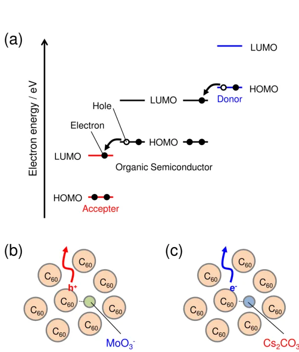
Fig. 1.3.2(a) shows schematic energy diagrams of cceptor and donor doped organic semiconductor. In the case of acceptor doping, the lowest unoccupied molecular orbital (LUMO) level of the dopant (red solid line) needs to be located below the highest occupied molecular orbital (HOMO) level of the organic semiconductor. The acceptor can withdraw an electron from the HOMO level of the organic semiconductor (black solid curve). On the other hand, in the case of donor doping, the HOMO level of the dopant (blue solid line) needs to be located above the LUMO level of the organic semiconductor. The donor can donate an electron to the LUMO level of the organic semiconductor (black solid curve). Thus, charge transport (CT) between the dopant and the organic semiconductor occurs due to the impurity doping.
Kubo et al. has confirmed that CT complexes form between fullerene (C60) and various dopants.36,37) It was found that two types of CT complex, i.e., C60+--- MoO3-
and C60---- Cs2CO3+, were formed in C60 films with acceptor (MoO3) and donor (Cs2CO3) dopants (Figs. 1.3.2(b) and (c)). These doped C60 films exhibited color changes and CT absorption. In addition, in the case of MoO3 doping, the Fermi energy (EF) shifted to the HOMO level. This suggests that the MoO3-doped C60 film was p-type. On the other hand, in the case of Cs2CO3 doping, EF shifted to the LUMO level, suggesting that the Cs2CO3-doped C60 film was n-type. Recently, Hiramoto et al. has reported on similar shifts in EF for various organic semiconductor films with impurity doping at a concentration of 3000 ppm.9) Thus, the mechanism of impurity doping can be explained by the CT model.
9
Moreover, the doping efficiency (I) can be calculated as the ratio of the number of carriers (Nfree carrier) created to that of the dopant molecule (Ndopant) by the following equation.
I =
�� � ��
(1.3.2.1)
In the case of inorganic semiconductors, due to the high permittivity such as 122), the doping efficiency reached 100%. However, in the case of organic semiconductors, due to the low permittivity such as 49), the doping efficiency was below 10% (Table. 1.3.2)39) and must be increased to 100%.
Table. 1.3.2 Doping efficiency for organic semiconductors
H2Pc C60
Accepter doping (FeCl3) 2 0.2
Donor doping (Cs2CO3) 10 10
10
Fig. 1.3.2 (a) Schematic energy band diagram of acceptor and donor doping in organic semiconductor. Schematic illustrations of (b) MoO3-doped and (c) Cs2CO3-doped C60 films.
(a)
HOMO
El ec tron energy / eV
Organic Semiconductor Electron
Hole
Accepter
Donor
HOMO LUMO
LUMO
HOMO LUMO
(b) (c)
C60
C60 C60
C60 C60
C60
C60 C60
C60
C60 C60
C60 C60
C60
C60 C60
MoO
3-Cs
2CO
3+h+ e-
11
1.3.3. Doped Organic Photovoltaic Cells
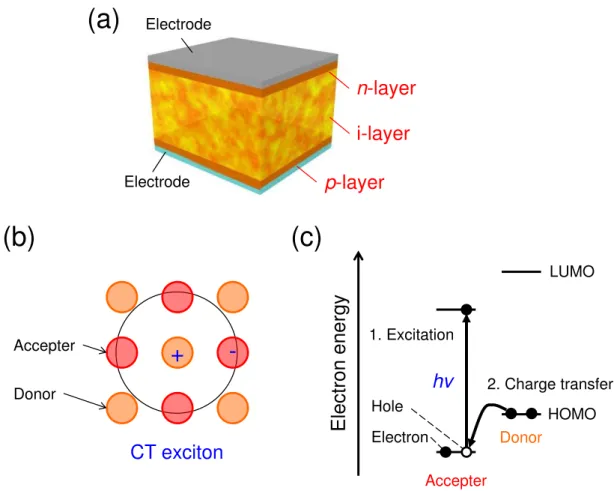
Organic photovoltaic cell (OPV) has been actively studied for next generation of solar cells. However, in an individual organic semiconductor film, the thickness of the photoactive layer and the photocurrent are limited by the exciton diffusion length of 10 nm.40,41) In order to improve photovoltaic performance, co-deposited films, i.e., blends of two types of organic semiconductor, have been developed (Fig. 1.3.3(a)).9,42) The photocurrent can be generated in the whole of the co-deposited film since charge transfer (CT) excitons dissociate at the interfaces between the acceptors (A) and donors (D) (Figs. 1.3.3(b), (c)) and then the electrons and holes are transported to the electrodes. Co-deposited films have been fabricated by the co-evaporation technique. This film structure can be optimized by the blend ratio, the evaporation rate and the heating temperature.43) For example, Sakai et al. has reported that the best blend ratio for fullerene and α-sexithiophene (C60:6T) in a co-deposited film is 10:1 due to it having a high open-circuit voltage (Voc) of 0.80 V.44)
Moreover, to further increase the power conversion efficiency (p), Ishiyama et al. reported on a tandem OPV.45-47) This cell was fabricated using only C60:6T films connected in series with two p+in+-homojunctions. Here, + means heavily doped. The values of Jsc, Voc and p increased from 4.5 mAcm-2, 0.85 V and 1.6% (for a single OPV) to 3.0 mAcm-2, 1.69 V and 2.4% (for a tandem OPV), respectively. Thus, impurity doping is an essential technique for enhancing photovoltaic performance.
12
Fig. 1.3.3 (a) Schematic diagram of a pin cell using a co-deposited film. (b) Charge transfer (CT) exciton model. (c) Mechanism of carrier generation in an organic photovoltaic cell.
(a)
(b)
Electrode
Electrode p-layer
n-layer i-layer
+ -
Accepter
Donor
CT exciton
(c)
Accepter
HOMO LUMO
Electron energy
Electron Hole
Donor
hv
1. Excitation
2. Charge transfer
13
1.4. Measurement Techniques for Doped Organic Semiconductors
1.4.1. Energy Band Mapping
Energy band mapping was used to measure carrier concentration (N) and was demonstrated using the thickness dependence of the work function (Φ). The work function of doped organic semiconductors can be measured by ultraviolet photoelectron spectroscopy (UPS)48) or by Kelvin probe (see chapter 2.3.2)49,50).
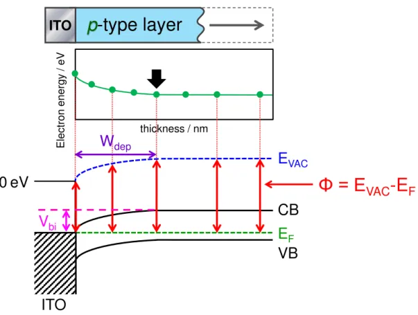
Fig. 1.4.1 shows the principle of energy band mapping utilizing a p-type Schottky junction.50) When an organic semiconductor is formed on an ITO substrate, the Fermi level (EF) of the p-layer is aligned with that of the ITO. Band bending occurs in the p-layer (black solid line). The thickness dependence of the work function directly shows the band bending because the work function is defined as the difference between the vacuum level and EF. The width of the depletion layer (Wdep) and the built-in potential (Vbi) are determined by the point at which the bands are no longer bent (black arrow). N can be calculated using equation 1.4.1.1.
N =
εε02 i(1.4.1.1)
where is the dielectric constant of the organic semiconductor, which is about 4. 0 is the permittivity of free space, which is 8.85 x 10⁻¹² Fm-1. In addition, the energy band structure of the p-type Schottky junction was found by turning the curves in Fig. 1.4.1 upside down. This principle is used in chapters 3 and 5.
14
Fig. 1.4.1 Typical principle of energy band mapping in a p-type Schottky junction.
CB
VB
thickness / nm
0 eV
ITO
ITO
p-type layer
E
VACW
depV
biE
FΦ = E
VAC-E
FElectron energy / eV
15
1.4.2. Hall Effect Measurements
The phenomenon of the Hall effect was discovered by Edwin Herbert Hall in 1879.51) Fig. 1.4.2 (a) shows schematic diagrams illustrating Hall effect measurements in a p-type organic semiconductor. When a magnetic field (B) (black mark) is applied perpendicular to the current (I) (blue solid line), the potential difference generated between the two electrodes by Lorentz force (green solid curve) as a result of this is called the Hall voltage (VH). The carrier concentration per unit volume (N, cm-3) can be determined from the following equation:
N =
H ∙(1.4.2.1)
Here, d is the thickness and RH is the Hall coefficient.
Positive and negative RH correspond to positive (p) and negative (n) type materials, respectively. In addition, not only N but also the Hall mobility (μH) can be determined using the Hall effect using the following equation:
μ�
=
σ�
� (1.4.2.2)where the carrier conductivity ( ) can be measured using the van der Pauw method. Trapped carriers make no contribution to μH since they cannot move under the influence of the Lorentz force (Fig. 1.4.2 (b)). Thus, μH is regarded as the intrinsic mobility without trap effect.
The standard method for separately and simultaneously determining N and μ in doped inorganic semiconductors is by making Hall effect measurements.51)
16
Fortunately, the Hall voltage of undoped rubrene single crystal, which possesses band-like transport properties, has been measured with the assistance of trap-healing11) and gate bias using a FET.12,13) The hole concentration per square centimeter (N□, cm-2) and μH were determined to be 1011 cm-2 and 10 cm2V-1s-1, respectively.13) However, the use of this method for doped organic single crystals without an FET has not, so far, been reported.
Fig. 1.4.2 (a) Schematic diagram illustrating Hall effect measurements. Models of (b) μH and (c) μD.
VB EA CB
μ
Hμ
DTrap CB
(a)
(b) (c)
Trap Acceptor ion
Hole
Current Lorentz force
Organic
semiconductor Electrode
X
Magnetic field Magnetic fieldAcceptor ion
Hole VB
EA
Current Lorentz force
17
1.4.3. Organic Field-Effect Transistors
An organic field-effect transistor (OFET) comprises three electrodes (gate (G), source (S) and drain (D)), a gate insulator and a channel layer. As shown in Fig. 1.4.3, there are four types of device structure for OFETs; (a) bottom-gate/top-contact, (b) bottom-gate/bottom-contact, (c) top-gate/top-contact, and (d) top-gate/bottom-contact. In particular, the bottom-gate and top-contact OFET ((a)) has been well employed because the fabrication process is simple to use the silicon substrate. When a gate-source voltage (VGS) is applied to an OFET, a source-drain current (ISD) flows (Figs. 1.4.3(e), (f)). The FET mobility (μFET) can be determined from equations 1.4.3.1 and 1.4.3.2. In the linear region,
I
D=
Lμ C { V − V
t� − � }
(1.4.3.1)In the saturation region,
I
D=
Lμ C V − V
t(1.4.3.2)
where W and L are the channel width and length, respectively. Ci is the capacitance per unit area of the gate dielectric layer and Vth is the threshold voltage.
μFET can be regarded as the drift mobility (μD). μD includes the effect of traps unlike the Hall mobility (μH) (Fig. 1.4.2(c)).
18
Fig. 1.4.3 (a), (b), (c), (d) Device structures of OFETs. (e) Transfer (IDS-VGS) and (f) output (IDS-VDS) characteristics.
Gate insulator G
Organic semiconductor
S D
Gate insulator G
Organic semiconductor
S D
Gate insulator G
Organic semiconductor
S D
Gate insulator G
Organic semiconductor
S D
(a) (b)
(c) (d)
1.E-09 1.E-08 1.E-07 1.E-06 1.E-05 1.E-04
0.E+00 2.E-03 4.E-03 6.E-03 8.E-03
-100-80 -60 -40 -20 0 20
-I
DS/ A
I
DS1/2/ A
1/2V
GS/ V
VDS=-100 V
-6.E-05
-5.E-05
-4.E-05
-3.E-05
-2.E-05
-1.E-05
0.E+00
-100 -80 -60 -40 -20 0
I
DS/ A
V
DS/ V
VGS=-100 V
VGS=-80 V
VGS=-60 V
VGS=-40 V VGS=-20 V
V
th(e) (f)
19
1.4.4. Organic Photovoltaic Cells
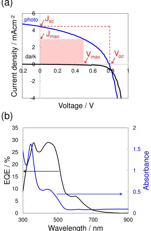
An organic photovoltaic cell (OPV) comprises two electrodes (anode and cathode) and a photoactive layer. When the photoactive layer is irradiated with solar light, a photocurrent is generated in the OPV. Fig. 1.4.4(a) shows typical J-V characteristics in the dark and under irradiation with simulated solar light. The power conversion efficiency (p) can be calculated using the following equation:
�
P=
PP xi
=
s ∙ ∙
Pi
(1.4.4.1)
Here, Jsc is the short-circuit photocurrent density, which is obtained from the value of J at V = 0V, and Voc is the open-circuit voltage, which is obtained from the value of V at J
= 0 mAcm-2. The fill factor (FF) can be calculated from the following equation:
FF =
P xs ∙
=
x ∙ x
s ∙
(1.4.4.2)
where Pmax is the maximum power output, which is obtained from the values of the current and voltage (Jmax and Vmax). Pin is the incident light intensity, which is usually used for AM 1.5G (100 mWcm-2).
Fig. 1.5.2(b) shows typical external quantum efficiency (EQE) of OPV. EQE can be calculated from the ratio of the number of carriers collected to the number of incident photons under the short-circuit condition as the following equation.
EQE =
N ��� � �ℎ (1.4.4.3)
20
Fig. 1.4.4 (a) Typical J-V characteristics in the dark and under irradiation with simulated solar light. (b) EQE of typical OPV.
-4 -2 0 2 4 6
-0.2 0 0.2 0.4 0.6 0.8 1
Current density / mAcm-2
Voltage / V
photo
dark
J
scV
ocJ
maxV
max(a)
(b)
Cu rr en t de nsi ty / mAcm
-20 0.5 1 1.5 2
0 5 10 15 20 25 30 35
300 500 700 900
Ab sorbance
EQE / %
Wavelength / nm
21
1.5. Motivation for This Doctoral Thesis
In this doctoral thesis, the author has focused on the development of a precise impurity doping technique at the ppm level both for organic thin films and organic single crystals. The main tasks undertaken were as follows.
(i) Effects of impurity doping in organic single crystals (chapters 3 and 4)
Doping to organic semiconductors have been performed in the amorphous and the polycrystalline films so far. However, the author believes that in order to precisely clarify the nature of the doping effects, doping organic single crystal without grain boundaries is necessary. When the impurity doping is applied to the single crystalline layers, the deposition rates of both the organic semiconductor and the dopant need to be minimized in order to suppress the structural defect. Thus, firstly, the author attempted to fabricate doped organic single crystals by means of an ultra-slow co-deposition technique. Secondly, the author attempted to demonstrate Hall effect measurements and organic field-effect transistors in doped organic single crystals for the first time.
(ii) Effects of impurity doping in organic photovoltaic cells (chapter 5)
In order to achieve a specific energy band structure, impurity doping is the standard technique for organic photovoltaic cells (see chapter 1.3.3). However, in conventional cells, the photocurrent is generated in an undoped co-deposited layer, i.e., the i-layer. The author believes that direct doping of a photoactive co-deposited layer provides us with the potential to enhance the photovoltaic performance. Thus, the author attempted to confirm this by using extremely low doping concentrations of 1 ppm for the first time.
22
1.6. Overview for This Doctoral Thesis
This thesis consists of six chapters.
In chapter 1, the background to the impurity doping of both inorganic and organic semiconductors and the motivation for carrying out the research work described in this thesis are presented.
In chapter 2, the experimental equipment and methods are described. Rubrene single crystals possessing band-like transport properties were employed for the Hall effect measurements. Co-deposited films of fullerene and α-sexithiophene (C60:6T) were used for the organic photovoltaic cells. Iron chloride (FeCl3) and cesium carbonate (Cs2CO3) were used for the accepter and donor dopants, respectively. Doped organic semiconductors were fabricated using a ‘multi-component co-evaporation’ technique. The deposition rates of the dopants were monitored using a quartz crystal microbalance equipped with a computer monitoring system. These rates were controlled using rotating shutters with aperture ratios of 1/10, 1/100, and 1/1000, which enabled us to control the doping concentration to as low as 1 ppm.
In chapter 3, the Hall effect measurements made on the doped organic single crystals is described. Also, the first successful achievement of the fabrication of a doped homoepitaxial single crystal layer on rubrene single crystal by an ultra-slow co-deposition technique is described. The minimum deposition rate for 1 ppm doping with FeCl3 was 10-9 nm s-1. A systematic study of both the hole concentration per unit volume (N, cm-3) and the Hall mobility (μH) of FeCl3-doped homoepitaxial rubrene single crystal was carried out using Hall effect measurements. With 100 ppm doping, N = 2.6 x 1017 cm-3 and μH = 1.4 cm2V-1s-1 were obtained. It was found that (i) the doping efficiency, i.e. the ionization rate of the acceptor dopant, of the rubrene single
23
crystal (24%) was higher than that of a rubrene vacuum deposited film (1.2%), which can be attributed to the lower concentration of hole traps and that (ii) there was a decrease in μH from 4.6 to 0.13 cm2V-1s-1 as the doping concentration was increased from 10 to 1000 ppm, which can be attributed to scattering effects due to lattice disturbances. These results are a first example of Hall effect measurements made on doped organic single crystals.
In chapter 4, the field-effect mobility of doped organic single crystals are described. FET mobility (μFET) can be regarded as the drift mobility (μD), which is dominated by hole traps. μD was about two-orders of magnitude less than the Hall mobility (μH). Since holes captured by traps cannot move under the influence of the δorentz force, μH contains no contribution from the trapped holes. So, we concluded that the lower μD values can be attributed to the effect of hole traps formed by lattice disturbances, which decrease the velocity of the holes by capturing them. The activation energy of the hole traps was determined to be 0.37 eV by measuring the temperature dependence of μD.
In chapter 5, the effects of impurity doping in simple n+p-homojunction organic photovoltaic cells are described. Here, + means heavily doped. The n+p-homojunctions were formed in C60:6T co-deposited films with acceptor (FeCl3) and donor (Cs2CO3) dopants. The doping concentration of FeCl3 in the p-layer was varied from 1 to 1000 ppm. The doping effects can be divided into three regions. Firstly, from 0 to 10 ppm, the fill factor (FF) increased due to the appearance of majority carriers (holes). Secondly, from 10 to 100 ppm, the photocurrent density (Jsc) increased due to an increase in the built-in potential, i.e., the formation of an n+p-homojunction. Thirdly, above 100 ppm, FF and Jsc decreased due to the decrease in hole mobility and
24
depletion layer width, respectively. Thus, we confirmed that the photovoltaic cell performance could be enhanced by the extremely low doping concentration of 1 ppm. In chapter 6, the conclusion to this thesis and prospects for the future are presented.
25
1.7. References
1) The Royal Swedish Academy of Sciences in the Nobel Prize in Physics 2014. 2) Physics of Semiconductor Devices, S. M. Sze, published by
WILEY-INTERSCEINCE, Chapter 2 (1969).
3) H. Akamatsu, H. Inokuchi, and Y. Mastunaga, Nature., 173, 168 (1954). 4) C. W. Tang, S. A. Vanslyke, Appl. Phys. Lett., 51 913 (1987).
5) C. W. Tang, Appl. Phys. Lett., 48 183 (1986).
6) K. Kudo, M. Yamashina, and T. Morizumi, Jpn. J. Appl. Phys., 23, 130 (1984). 7) Physics of Organic Semiconductors, W. Brutting, edited by WILEY-VCH Verlag
GmbH & Co. KGaA, Chapter 1 (2005). 8) Sony corporation in 2007.
9) M. Hiramoto, M. Kubo, Y. Shinmura, N. Ishiyama, T. Kaji, K. Sakai, T. Ohno, and M. Izaki, Electronics., 3, 351 (2014).
10) B. Luussem, C.M. Keum, D. Kasemann, B. Naab, Z. Bao, and Karl Leo, Chem. Rev.,116, 13714 (2016).
11) B. Lee, Y. Chen, D. Fu, H. T.Yi, K. Czelen, H. Najafov, and V. Podzorov, Nat. Mater., 12, 1125 (2013).
12) V. Podzorov, E. Menard, J. A. Rogers, and M. E. Gershenson, Phys. Rev. Lett., 95, 226602 (2005).
13) J. Takeya, J. Kato, K. Hara, M. Yamagishi, R. Hirahara, K. Yamada, Y. Nakazawa, S. Ikehata, K. Tsukagoshi, Y. Aoyagi, T. Takenobu, and Y. Iwasa, Phys. Rev. Lett., 98, 196804 (2007).
14) Physics of Semiconductor Devices, S. M. Sze, published by WILEY-INTERSCEINCE, Chapter 3 (1969).
26
15) Ge. R. Hutchison, M. A. Ratner, and T. J. Marks, J. Am. Chem. Soc., 127, 2339 (2005).
16) T. Kanbara, K. Shibata, S. Fujiki, Y. Kubozono, S. Kashino, T. Urisu, M. Sakai, A. Fujiwara, R. Kumashiro, and K. Tanigaki, Chem Phys Lett., 379, 223 (2003).
17) M. Hiramoto, K. Ihara, H. Fukusumi, and M. Yokoyama, J. Appl. Phys., 78, 7153 (1995).
18) M. Maitrot, G. Guilland, and B. Boudjema, J. J. Andre, and J. Simon, J. Appl. Phys., 60, 2396 (1986).
19) E. J. Lous, P. W. M. Blom, L. W. Molenkamp, and D. M. Leeuw, Phys. Rev. B., 51, 17251 (1995).
20) M. L. Tietze, P. Pahner, K. Schmidt, K. Leo, and B. Lussem, Adv. Funct. Mater., 25, 2701 (2015).
21) M. Kroger, S. Hamwi, J. Meyer, T. Riedl, W. Kowalsky, and A. Kahn, Org. Electron., 10, 932 (2009).
22) M. Kubo, Y. Shinmura, N. Ishiyama, T. Kaji, and M. Hiramoto, Mol. Cryst. Liq. Cryst., 581 13 (2013).
23) J. Endo, T. Matsumoto, and J. Kido, Jpn. J. Appl. Phys., 41, 358 (2002).
24) D. L. Price, M. L. Saboungi, and Y. S. Badyal, Phys. Rev. B., 57, 10496 (1998). 25) G. Parthasarathy, C. Shen, A. Kahn, and S. R. Forrest, J. Appl. Phys., 89, 4986
(2001).
26) C. K. Chiang, S.C. Gau, C. R. Fincher, Jr,, Y. W. Park, A. G. MacDiarmid, and A. J. Heeger, Appl. Phys. Lett., 33, 18 (1978).
27) T. Takenobu, T, Takano, M, Shiraishi, Y, Murakami, M, Ata, H, Kataura, Y, Achiba and Y. Iwasa, Nat. Mater., 2, 68 (2003).
27
28) M. Chikamatsu, T. Taima, Y. Yoshida, K. Saito, and K. Yase, Appl. Phys. Lett., 84, 128 (2004).
29) M. Kubo, T. Kaji, and M. Hiramoto, AIP Advances., 1, 032177 (2011).
30) H. H. Liao, L. M. Chen, Z. Xu, G. Li, and Y. Yang, Appl. Phys. Lett., 92, 173303 (2008).
31) N. Ishiyama, M. Kubo, T. Kaji, and M. Hiramoto, Appl. Phys. Lett., 101, 233303 (2012).
32) E. J. Meijer, D. M. Deleeuw, S. Setayesh, E. V. Veenendaal, B. H. Huisman, P. W. Blom, J. C. Hummelen, U. Scherf, and T. M. Klapwijk, Nat. Mater., 2, 678 (2003). 33) R. W. I. deBoer, A. F. Stassen, M. F. Craciun, C. L. Mulder, A. Molinari, S. Rogge,
and A. F. Morpurgoa, Appl. Phys. Lett., 86, 262109 (2005).
34) Y. Takahashi, T. Hasegawa, Y. Abe, Y. Tokura, and G. Saito, Appl. Phys. Lett., 88, 073504 (2006).
35) A. Dodabalapur, H. E. Katz, L. Torsi and R. C. Haddon, Appl. Phys. Lett., 68, 1108 (1996).
36) M. Kubo, K. Iketaki, T. Kaji, and M. Hiramoto, Appl. Phys. Lett., 98, 073311 (2011).
37) M. Kubo, T. Kaji, and M. Hiramoto, AIP Advances., 1, 032177 (2011).
38) D. L. Price, M. L. Saboungi, and Y. S. Badyal, Phys. Rev. B., 57, 10496 (1998). 39) Y. Shinmura, Y. Yamashina, T. Kaji, and M. Hiramoto, Appl. Phys. Lett., 105,
183306 (2014).
40) P.Peumans, A. Yakimov, and S.R. Forrest, J. Appl. Phys., 93, 3693 (2003).
41) M. Hiramoto, T. Yamaga, M. Danno, K. Suemori, Y. Matsumura, and M. Yokoyama, Appl. Phys. Lett., 88, 213105 (2006).
28
42) M. Hiramoto, H. Fujiwara1 and M. Yokoyama, J. Appl. Phys., 72, 3781 (1992). 43) T. Kaji , M. Zhang , S. Nakao , K. Iketaki , K. Yokoyama , C. W. Tang , and M.
Hiramoto, Adv. Mater., 23, 3320 (2011).
44) J. Sakai, T. Taima, and K. Satio, Organic Electronics, 9, 582 (2008).
45) N. Ishiyama, M. Kubo, T. Kaji, and M. Hiramoto, Appl. Phys. Lett., 101, 233303 (2012).
46) N. Ishiyama, T. Yoshioka, T. Kaji, and M. Hiramoto, Appl. Phys. Express., 6, 012301 (2013).
47) N. Ishiyama, M. Kubo, T. Kaji, and M. Hiramoto, Org. Electron., 14, 1793 (2013). 48) J. Blochwitz, T. Fritz, M. Pfeiffer, K. Leo, D.M. Alloway, P.A. Lee, and N.R.
Armstrong, Org. Electron., 2, 97 (2001).
49) Y. Shinmura, T. Yoshioka, T. Kaji, and M. Hiramoto, Appl. Phys Express., 7, 071601 (2014).
50) Y. Yamashina, Y. Shinmura, N. Ishiyama, T. Kaji, and M. Hiramoto, J. Appl. Phys., 117, 125501 (2015).
51) Physics of Semiconductor Devices, S. M. Sze, published by WILEY-INTERSCEINCE, Chapter 3 (1969).
29
Chapter 2:
Experimental Equipment and Methods
2.1. Purification of Organic Semiconductors
-sexithiophene (6T) (Tokyo Chemical Industry), rubrene (Tokyo Chemical Industry) and fullerene (C60) (Frontier Carbon, nanom purple TL) were purified by single crystal sublimation (Fig. 2.1) (EpiTech Inc).1,2) The sublimation purifier had three temperature zones, high (green) at one end, low (blue) at the other end, and moderate (red) in between. The samples were put into the high temperature end near the heat source and were evaporated in the quartz tube under N2 flow. Highly purified single crystals (99.99999%) were separated from the impurities in the moderate and low temperature zones utilizing the difference in deposition temperatures. Organic single crystals several millimeters in size were grown. Details of the sublimation conditions used to prepare these highly purified organic semiconductors are given in Table 2.1.
The acceptor dopants, iron(III) chloride (FeCl3) (Sigma-Aldrich, 99.99%)3,4), and the donor dopant, cesium carbonate (Cs2CO3) (Sigma-Aldrich, 99.995%)5,6), were used without further purification. Aluminum (Al) (New Metals & Chemicals Ltd, 99.999%) and gold (Au) (Nilaco, 99.95%) were used for the electrodes.
30
Fig. 2.1 Single crystal sublimation of highly purified organic semiconductors.
Table 2.1 Sublimation conditions.
Sample Temperature /
oC Heating time / h
High Middle Low
6T 320 250 170 1
Rubrene 320 250 170 1
C
60745 580 310 36
N
2flow
Middle High
Low
Single crystal
Sample
Impurity
31
2.2. Extremely Low Concentration Doping for Organic
Semiconductors
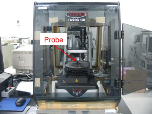
Doping for the organic semiconductors was performed using a multi-component co-evaporation technique as shown in Fig. 2.2.1.2) The evaporation sources were prepared in melting pots of aluminum oxide (Al2O3) (Nilaco, C-1). All materials were independently evaporated using tungsten basket resistance heaters (Nilaco, BH-1) under vacuum ( > 10-5 Pa). The deposition rates were controlled using quartz crystal microbalances (QCMs) (INFICON, 750-1050-G10) connected to a computer monitoring system (ULVAC, CRTM-9000G/Depoview). The thicknesses of the deposited films were measured by a surface profiler (Fig. 2.2.3) (Veeco, Dektak150). The actual thicknesses were determined using a tooling factor.
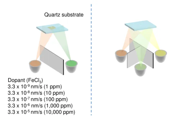
Fig. 2.2.2 shows a typical example of the dependence of the dopant thickness on the deposition time at a deposition rate of 1.0 x 10⁻⁵ nm s-1. The observed cyclic fluctuations were caused by temperature variations in the coolant water for the QCMs. The deposition rate can be estimated from the gradient of the baseline (red). As the deposition rates of the organic semiconductor and the dopant were 1.0 and 1.0 x 10⁻⁵ nm s-1, respectively, the doping concentration was 100 ppm. Extremely low doping concentrations of 10 and 1 ppm were realized by reducing the dopant evaporation rate using rotating disks containing slits with aperture ratios of 1:10 and 1:100, respectively (Fig. 2.2.4). In addition, in order to grow homoepitaxial films on the single crystal substrate, rubrene was deposited at a low evaporation rate of 3.3 x 10⁻³ nm s-1 at room temperature (Fig. 2.2.1 (a)).7)
The minimum deposition rate for 1 ppm doping with dopant (FeCl3) was 3.3 x 10⁻⁹ nm s-1.
32
Fig. 2.2.1 Illustration showing (a) ‘Two-component co-evaporation technique’ and (b)
‘Three-component co-evaporation technique’.
Fig. 2.2.2 Typical dependence of dopant thickness on deposition time at a rate of 1.0 x 10⁻⁵ nm s-1.
Quartz substrate
Dopant (FeCl3)
3.3 x 10⁻⁹ nm/s (1 ppm) 3.3 x 10⁻⁸ nm/s (10 ppm) 3.3 x 10⁻⁷ nm/s (100 ppm) 3.3 x 10⁻⁶nm/s (1,000 ppm) 3.3 x 10⁻⁵ nm/s (10,000 ppm)
Rubrene single crystal
Rubrene 3.3 x 10⁻³nm/s
ITO substrate
6T
10-2nm/s
C60 10-1nm/s
Dopants (FeCl3, Cs2CO3) 1.1x10⁻⁷ nm/s (1 ppm) 1.1x10⁻⁶ nm/s (10 ppm) 1.1x10⁻⁵ nm/s(100 ppm) 1.1x10⁻⁴ nm/s(1,000 ppm) 1.1x10⁻³ nm/s(10,000 ppm)
(a) (b)
3 3.1 3.2 3.3
5000 6000 7000 8000 9000 10000
Dopa nt thi ck ne ss / k Å
Deposition time / s
Deposition rate:1.0x10⁻⁵ nm/s
0 1000 2000 3000 4000 5000
0 0.1 0.2 0.3
33
Fig. 2.2.3 Surface profiler for measuring thickness.
Fig. 2.2.4 Rotating disk containing slits with an aperture ratio of 1:10 for extremely low concentration doping.
Probe
Evaporation source
Slit (aperture ratio of 1/10)
Rotating
34
2.3. Measurements of Doped Organic Semiconductors
2.3.1. Hall effect Measurements
Hall effect measurements8-10) were performed as shown in Fig. 2.3.1.1. The samples were fabricated on quartz substrates. Doping for the organic semiconductors was performed using the multi-component co-evaporation technique (see section 2.2), and electrodes were evaporated onto the organic thin films through a metal mask. The distance between the electrodes (L) was 50 μm. To prepare ohmic contacts, heavily doped layers were fabricated beneath the electrodes.11)
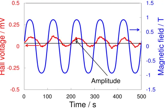
Fig. 2.3.1.2 shows a typical example of the variation of the Hall voltage with the magnetic field. The Hall voltage (VH) is obtained from the amplitude, as shown in the figure. The Hall coefficient (RH) can be determined from the following equation:
R =
H ∙ B ∙(2.3.1.1)
where d is the film thickness, and I and B are the current and magnetic flux density, which were usually 1.0 x 10⁻⁷ A and ±1 T, respectively.
The carrier concentration per unit volume (N, cm-3) and mobility (cm2V-1s-1) were determined by the observed RH (detail in chapter 1.4.2).
35
Fig. 2.3.1.1 Hall-effect measurement using the van der Pauw method
Fig. 2.3.1.2 Typical variation of the Hall voltage with the magnetic field. Sample
Magnet
-1.5 -1 -0.5 0 0.5 1 1.5
-0.5 -0.25 0 0.25 0.5
500 600 700 800 900 1000
Mag ne tic fie ld / T
Hall v ol tag e / mV
Time / s
Amplitude
0 100 200 300 400 500
36
2.3.2. Kelvin Probe Measurements
The Fermi energy (EF) for undoped and doped organic semiconductors was observed using the Kelvin Probe method (Riken Keiki, FAC-1).12) Since the value of EF is sensitive to air, all the samples were fabricated in a glove box (Fig. 2.3.2.1), in which the concentrations of water (H2O) and oxygen (O2) were kept to 0.5 and 0.2 ppm, respectively. Fig. 2.3.2.2(a) shows the setup for this measurement.13) When the film is brought into contact with a standard gold (Au) plate, the Fermi levels shift to become aligned (Fig. 2.3.2.2(b)), and a potential difference (ΔΦ), equivalent to the metal work function difference, forms at the interface between the organic semiconductor and the gold. To make the measurement, an alternating current (AC) is generated in the circuit by vibrating the plate. The value of ΔΦ is measured from the voltage required to cancel the alternating current (Q = 0) (Fig. 2.3.2.2(c)). Since the work function of Au is known to be 4.40 eV, the position of EF in the organic semiconductor can be simply determined from ΔΦ.
37
Fig. 2.3.2.1 Kelvin probe measurements in a glove box.
Fig. 2.3.2.2 (a) Setup for the Kelvin probe measurements. (b) Energy band diagram with Fermi levels aligned. (c) Energy band diagram with Q = 0.
Stage
Au plate
A
~
Gold plate Sample
Q -Q
(a)
EF EF
Q -Q ΔΦ
(c)
EF
(b)
ΔΦ EF Q = 0
38
2.3.3. Organic Field-Effect Transistors
The transfer (IDS-VGS) and output (IDS-VDS) characteristics of a Field-Effect Transistor (FET) were measured using a semiconductor characterization system (KEITHLEY, 4200-SCS) as shown in Fig. 2.3.3.
Bottom gate and top contact Field-Effect Transistors (FET) were fabricated on heavily n-doped silicon substrates. Electrodes were evaporated onto the organic thin films through a metal mask. The channel width (W) and length (L) were 1.0 mm and 50 μm, respectively. To prepare ohmic contacts, heavily doped layers were fabricated beneath the electrodes.11)
Fig. 2.3.3 Semiconductor characterization system for FET measurements.
Sample box
Semiconductor characterization system
39
2.3.4. Organic Photovoltaic Cells
In the case of the photovoltaic properties, the cells were firstly fabricated on patterned indium tin oxide (ITO) substrates. Electrodes were evaporated onto the organic thin films through a metal mask with an aperture area of 0.06 cm2. To measure the photovoltaic properties, all the cells were set into a sample container with a quartz glass window and electrical connecting ports (EpiTech Inc) as shown in Fig. 2.3.4.1. The container was evacuated to 10-3 Pa during the measurements. The photo-irradiated area was precisely defined by a photomask with an aperture area of 0.04 cm2.
Current density-voltage (J-V) measurements with a solar simulator (AM1.5, 100 mWcm-2) (USHIO INC, MS110AAA), as shown in Fig. 2.3.4.2, were made in order to determine some of the photovoltaic properties. Other photovoltaic properties were observed using the action spectrum measurement system shown in Fig. 2.3.4.3. The external quantum efficiency (EQE) can be calculated from the ratio of the number of carriers collected to the number of incident photons under the short-circuit condition. The number of carriers was measured by irradiating the cells with a Xe-lamp through a monochromator (Shimadzu, SPG-3ST). The number of incident photons was measured by the same method using a silicon photodiode (Hamamatsu Photonics, S1337-66BQ).
40
Fig. 2.3.4.1 Setting the cells into the sample container for measurement of the photovoltaic properties.
Fig. 2.3.4.2 J-V measurement with a solar simulator. Quartz glass window Electrical connecting ports Photomask Cell
0.04 cm2
Photo irradiation
(AM 1.5G, 100 mWcm
-2)
Cell sample
To vacuum pump
41
Fig. 2.3.4.3 Action spectrum measurement system.
Cell sample
Xe-lamp
Monochromator
Shutter
42
2.3.5. Thin-film Structures
Thin film structures were observed using an optical microscope (Nikon, ECLIPSE ME600) and an Atomic Force Microscope (AFM) (Seiko Instruments, SPI3800) as shown in Fig. 2.3.5.1. The AFM images were measured using a rhodium micro cantilever (EpoLead, SI-DF3-R) in dynamic mode with a resonant frequency of 25 kHz. In addition, the crystal structures were characterized by Grazing Incidence X-ray Diffraction (GIXD) (Rigaku, D/εAX RAPID II) using CuKα radiation generated by a voltage of 40 KV with a current of 30 mA as shown in Fig. 2.3.5.2.14) Most of the samples for this were prepared on quartz substrates without electrodes.
Fig. 2.3.5.1 Optical Microscope and AFM used for the measurements. Optical Microscope Atomic Force Microscope
Stage Stage
43
Fig. 2.3.5.2 GIXD measurement system.
Imaging plate
Light source
44
2.4. References
1) R.A. Laudise, Ch. Kloc, P.G. Simpkins, and T. Siegrist, J. Cryst. Growth., 187, 449 (1998).
2) M. Hiramoto, M. Kubo, Y. Shinmura, N. Ishiyama, T. Kaji, K. Sakai, T. Ohno, and M. Izaki, Electronics., 3, 351 (2014).
3) J. Endo, T. Matsumoto, and J. Kido, Jpn. J. Appl. Phys., 41, 358 (2002).
4) Y. Shinmura, Y. Yamashina, T. Kaji, and M. Hiramoto, Appl. Phys. Lett., 105, 183306 (2014).
5) M. Kubo, Y. Shinmura, N. Ishiyama, T. Kaji, and M. Hiramoto, Mol. Cryst. Liq. Cryst., 581, 13 (2013).
6) M. Kubo, T. Kaji, and M. Hiramoto, Appl. Phys. Lett., 103, 263303 (2013).
7) X. Zeng, L. Wang, L. Duan, and Y. Qiu, Crystal Growth & Design., 8, 1617 (2008).
8) V. Podzorov, E. Menard, J. A. Rogers, and M. E. Gershenson1, Phys. Rev. Lett., 95, 226601 (2005).
9) J. Takeya, K. Tsukagoshi, Y. Aoyagi, T. Takenobu and Y. Iwasa, Jpn. J. Appl. Phys., 44, 1393 (2005).
10) K. Noda, A. Sugawara, T. Wakahiki, K. Okamoto, T. Kiyosu, K. Matsushige, and Y. Wada, IEEJ Trans. EIS., 132, 1398 (2012).
11) M. Kubo, Y. Shinmura, N. Ishiyama, T. Kaji, and M. Hiramoto, Appl. Phys Express., 5, 092302 (2012).
12) Y. Shinmura, T. Yoshioka, T. Kaji, and M. Hiramoto, Appl. Phys Express., 7, 071601 (2014).
13) Physics of Organic Semiconductors, W. Brutting, edited by WILEY-VCH Verlag
45 GmbH & Co. KGaA, Chapter 3 (2005).
14) M. Izaki, T. Saito, T. Ohata, K, Murata, B. M. Fariza, J. Sasano, T. Shinagawa, and S. Watase, ACS Appl. Mater., 4, 3558 (2012).
46
Chapter 3:
Hall effect in Doped Organic Single Crystals
“Hall effect in doped organic single crystals”, Chika Ohashi, Yusuke Shinmura, Seiji Watase, Masanobu Izaki, Hiroyoshi Naito, Seiichiro Izawa, and Masahiro Hiramoto, Adv. Mater., DOI: 10.1002/adma.201605619.
Abstract
The standard technique to separately and simultaneously determine the carrier concentration per unit volume (N, cm-3) and the mobility (μ) of doped inorganic single crystal is to measure the Hall effect. However, this has not been reported for doped organic single crystal. Here, we report on the Hall effect measurements in doped single crystal organic semiconductors. A key feature of this work is the ultra-slow co-deposition technique reaching as low as 10-9 nm s-1, which enables us to dope homoepitaxial organic single crystal with acceptors at extremely low concentrations down to 1 ppm. Both the hole concentration per unit volume (N, cm-3) and the Hall mobility (μH) of doped rubrene single crystal, which has a band-like nature, were systematically observed. We found that the rubrene single crystal had (i) a high ionization rate and (ii) scattering effects due to lattice disturbances, which are peculiar to this organic single crystal.
47
3.1. Introduction
Doping is indispensable for organic semiconductor devices such as photovoltaic cells1-3) and field-effect transistors (FET)4-6). Recently, the effects of ultralow doping of vacuum deposited organic semiconductor films have been reported.7-9) We previously reported the effects of doping at concentrations down to 1 ppm in organic photovoltaic cells with simple pn-homojunctions.10) We think that in order to precisely clarify the nature of the doping effects, doping organic single crystal without grain boundaries is necessary.
A key feature of this work is an ultra-slow co-deposition technique reaching 10-9 nm s-1, which allows the successful doping of acceptors at extremely low concentrations down to 1 ppm in organic single crystal.
For doped inorganic single crystal, making Hall effect measurements is a standard technique, and is used to separately and simultaneously determine the carrier concentration per unit volume (N, cm-3) and the mobility (μ).11) However, there haven’t been any reports of these measurements being made on doped organic single crystal. Fortunately, the Hall voltage of undoped rubrene single crystal, which possesses band-like transport properties, has been measured with the assistance of trap-healing12) and gate bias using a FET.13,14) We expected that if doped rubrene single crystal could be fabricated, the Hall voltage could be measured. It should be noted that, in the case of doped organic single crystal, the carrier concentration per unit volume (N, cm-3) should be determined, though, so far, attention has been paid only to the carrier concentration per unit square (N□, cm-2).
In this chapter, we report on a demonstration of Hall effect measurements in doped homoepitaxial rubrene single crystal. This sample was fabricated by
48
homoepitaxial growth on rubrene single crystal substrates. The homoepitaxial layer can be grown at a slow evaporation rate15) and can be doped by means of the co-deposition technique.3) For the lowest doping concentration of 1 ppm, we developed an extremely slow evaporation rate of 10-9 nm s-1. Iron chloride (FeCl3) was used as the acceptor dopant.
49
3.2. Experimental
3.2.1. Homoepitaxial Cells
Rubrene single crystal (Tokyo Chemical Industry) was grown by physical vapor transport in N2 (0.1 atm) using train sublimation apparatus (EpiTech Inc.).16,17) The typical thickness of the samples was around 5 μm. Fig. 3.3.1(a) shows an optical microscope image of a device used for Hall effect measurements. Four square 50 nm-thick Au electrodes in a van der Pauw configuration were deposited on the rubrene single crystal. The gaps between the electrodes are 50 μm.18) The electrodes are arranged parallel to the a- and b-axes at the (001) surface.19)
Fig. 3.3.1(c) shows a cross section of the device. In order to grow homoepitaxial films on the single crystal substrate, rubrene was deposited at a low evaporation rate of 3.3 x 10⁻³ nm s-1 at room temperature15) using an oil-free vacuum evaporator (EpiTech Inc., ETVP-VG 100-SP) housed in a glove box (EpiTech Inc., 12ET12007). The typical thickness was 20 nm. 10 nm thick vacuum deposited p+-rubrene films heavily doped with FeCl3 at a concentration of 10000 ppm were inserted between the Au electrodes and the crystal (Fig. 3.3.1(c)).