A N
EWC
LASS OFE
ASILYT
ESTABLEA
SSIGNMENTD
ECISIOND
IAGRAMSNorlina Paraman, Chia Yee Ooi*, Ahmad Zuri Sha’ameri*, Hideo Fujiwara+
Faculty of Electrical Engineering, Universiti Teknologi Malaysia, 81310 Skudai Johor Malaysia
Graduate School of Information Science, Nara Institute of Science and Technology, Kansai
Science City, 630-0192 Japan.
*{norlina,ooichiayee,zuri}@fke.utm.my, [email protected]
ABSTRACT
This paper introduces a new class of assignment decision diagrams (ADD) called thru-testable ADDs based on a testability property called thru function. The thru-testable ADDs is an easily-testable set of thru functions that allows data transfer from its input to its output. We also define a design-for-testability (DFT) method to augment a given ADD with thru functions so that the ADD becomes thru-testable. We compare the circuits modified using our proposed method with the original circuits and partial scan designed circuits in terms of fault efficiency, area overhead, test generation time and test application time. Since the proposed DFT method is introduced at a high level, which deals with less number of gates, the information of thru functions can be extracted more easily. As a result, it lowers the area overhead compared to partial scan.
Keywords: Assignment Decision Diagram (ADD); Thru-testable; Design-For-Testability (DFT); Digital testing
1.0 INTRODUCTION
With the advance in semiconductor technology, the complexity of Very Large Scale Integration (VLSI) designs is growing and the cost of testing is increasing. Therefore, it is necessary to reduce the cost but enhance the quality of testing. The cost of testing depends mainly on the test generation time and test application time. The quality of testing is measured by fault coverage. Therefore, we have to reduce test generation time and test application time while enhancing fault efficiency. In order to reduce the complexity of the test generation for a circuit, a design-for- testability (DFT) method is introduced [1-2]. The previous DFT methods are summarized in the following subsections.
1.1 Design-for-testability at Gate Level
Various DFT methods have been proposed to augment a given circuit to make it more easily testable. The most commonly used DFT method is the scan technique (full or partial) [3-5]. However, the area overhead of a full scan technique is large because all flip-flops are augmented and chained together into a scan path. Another disadvantage of this technique is long test application time, which is a result of the shifting of test vectors through the scan chain. Therefore, the cost of testing using the full scan technique increases due to the large area overhead and long test application time. In order to reduce the area overhead, a partial scan technique has been proposed in which only a subset of the flip-flops is included in the scan path. It can save an area overhead while maintaining high fault coverage. In a partial scan, the scan flip-flop selection is based on the concept of minimum feedback vertex set (MFVS), where only a minimum number of flip-flops is selected to be scanned. However, the DFT at the gate level deals with a huge number of gates that may incur a higher area overhead.
1.2 Design-for-testability at High Level
By applying the DFT method at a high level, the number of primitive elements to be dealt with in the circuit is reduced [6]. Moreover, DFT at high level can be applied in the early design phase to reduce the area overhead. Moreover, the information extraction from a high level description is much faster than that from a gate level netlist. Several non-scan DFT methods at RTL which use normal data path flow as a scan path have been proposed. These methods reduce hardware overhead and test application time compared with the full scan design. However, the
Malaysian Journal of Computer Science, Vol. 23(1), 2010 1
test generation time cannot be reduced because the test generation approach is the same as the full scan design. In the H-scan technique [7], some extra gates are added to the logic of the existing path so that signals transferred between the registers is enabled by a new input independent on the signals from the controller.
The design-for-testability based on strong testability in [8-9] is guaranteed to generate test plans for all combinational hardware elements of the data path. However, the DFT methods in [8-10] assumed that a controller and a data path are separated from each other and the signal lines between them are directly controllable and observable from the outside of circuits. Therefore, extra multiplexers are added to the signal lines in between a controller and a data path, and an extra test controller is also embedded to provide the test plans for the data path. The method in [11] allows speed testing and achieves a much shorter test application time compared to the full scan approach. However, the hardware and delay overheads are larger compared to the full scan approach because of the extra multiplexers and test controller.
The previous works show that DFT methods treat data path and controller separately. In fact, they need the insertion of additional hardware, like a test controller to control the data transfer from the primary input to the targeted fault and from the targeted fault to the primary output. In this paper, we introduce a new DFT method using a high level modeling known as Assignment Decision Diagram (ADD) [13] extended from the previous work that has been done in [12]. Different from [12], we abstract the DFT from the gate level and extend it to RTL. Additionally, our DFT method treats data path and controller unanimously. The DFT method augments a given RTL circuit based on the testability properties called thru function. We extract the thru function from the high level description of a given RTL circuit. Our method will improve test generation time and test application time as well as fault efficiency.
This paper is organized as follows. In Section 2, we briefly review ADD. We present how to extract thru function from ADD and define a representation of ADD called R-graph. We also define a new concept of special class of ADDs called thru-testable ADD. In Section 3, we describe the test generation model for thru-testable ADD. In Section 4, we present the DFT method to augment a given ADD with thru functions so that the ADD becomes thru-testable. Experimental results are presented in Section 5 and the conclusions are in Section 6.
2.0 PRELIMINARIES
2.1 Assignment Decision Diagram (ADD)
ADD is the modeling of behavioral description that has been proposed previously for high level synthesis [13-16]. The ADD representation consists of four parts: the assignment value, the assignment condition, the assignment decision and the assignment target. These parts are implemented with four types of nodes: read nodes, operation nodes, write nodes and assignment decision nodes (ADN).
The assignment value part consists of read nodes and operation nodes. This part represents the computation of values that are to be assigned to a storage unit or output port. This value is computed from the current contents of the input ports or storage element or constants which are all represented by the read nodes. The assignment condition part consists of read nodes and operation nodes that are also connected as a data-flow graph. The end product of the computation is a Boolean value which is the guarding condition for the assignment value.
The assignment decision part consists of an ADN. The ADN selects a value form a set of values that are provided at its value inputs. If one of the conditions to the ADN evaluates to true, then the corresponding input value is selected. The assignment target is represented by a write node. The write node is associated with the selected value from the corresponding ADN. A value is assigned to the write node only if one of the condition inputs to the ADN evaluates to true. Although ADD was essentially introduced as an internal representation in the high level synthesis process, it can be used to describe a functional RTL circuit, the controller part and the data path part of which are homogeneously represented.
2.2 Thru Function
Thru function is an important property of a thru-testable ADD. A thru function is a logic that transfers the same signals from the input to the output if the thru function is active. The bit width of the input and output are equal. We
Malaysian Journal of Computer Science, Vol. 23(1), 2010 2
Malaysian Journal of Computer Science, Vol. 23(1), 2010 3
define the following definition to describe the thru function concept.
Definition 1. Let X, Y and Z be a set of variables respectively in ADD where X∩Z= and Y∩Z= . A thru function tXY is a logic, equality, relational and arithmetic operations such that
1. the operations connectives of the function consist of (AND), (OR) and ¬(NOT), < (LESS THAN), > (MORE THAN) and = (EQUAL);
2. the operation variables Z of the function and X consist of read nodes while Y consists of write nodes;
3. the signals at X transfer to Y if Z has an assignment that makes the thru function ‘true’ or active ( tX Y=1).
Note that X and Y may have the same variables that make the thru function transfers the signal from one variable to the same variable. This thru function is called self thru function.
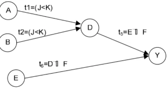
Example 1: Fig. 1 shows two examples of thru functions. Two thru functions are independent if they cannot be activated at the same time. Fig. 1(a) shows that thru functions tA B and tCB are dependent. Dependent thru functions transfer signal at the same time and activated by same variable. In this case, signals from A and C are transferred to B at the same time when a1 is true. Fig. 1(b) shows that thru functions, tA B and tCB are independent. This means data transfer from A to B cannot happen at the same time as data transfer from C to B. The former takes place when a1 is true.
I J
B
A C A
B C
a1
a1 a2
(a) (b)
Fig. 1. Thru functions 2.3 R-graph
To facilitate the implementation of our DFT method, we introduce a graph representation called R-graph, which contains the information of connectivity, thru function of an ADD. R-graph is defined as an ADD representation by using read nodes as input and write nodes as output. The R-graph includes ADD properties of thru function, thru tree and input dependency. Based on these properties, the class of thru-testable ADDs is defined.
Definition 2. An R-graph of an ADD is a directed graph G=(V,A,w,t) that has the following properties.
1. v V is a read node or write node. If a read node and a write node correspond to the same variable, they are represented by the same vertex;
2. (vi, vj) A denotes an arc if there exists a path from the read node vi to the write node vj;
3. w:V→Z+ (the set of positive integers) defines the size of read or write node corresponding to a vertex in V;
4. t:A→T {0,1} (T is a set of thru functions) where t(u,v)=0 if there is no thru function for (u,v) A and t(u,v) is a thru function that transfers signals from the read node u to the write node v. If t(u,v)=1 (also called identity thru function), the signal values are transferred from u to v directly. Note that identity thru function is always active.
Fig. 2. ADD S1
Fig. 3. An R-graph for ADD S1
Example 1: Fig. 3 shows the R-graph of the ADD S1of Fig. 2. Read nodes A, B, E, J, K, S, T, M, N, and F are primary inputs while write node Y is primary output. An arc exists from the read node to the write node. For example, arc (A,D) exists in the R-graph because there exists a path from read node A to write node D through an assignment decision node (ADN). According to the R-graph, node D forms a self thru function. Note that vertices S, T, M and N are assignment indices.
2.4 Thru Testability
The thru-testable ADD is a class of ADDs that is easily testable. The class of thru-testable ADDs is defined below. Before defining the thru-testable ADD, we visualize a certain set of thru functions as a thru tree using R-graph representation, which is defined as follows.
Definition 3. A thru tree is a sub graph of the R-graph such that: 1. it is a directed rooted tree;
2. there is only one sink (root) with no outgoing arcs;
3. the sources are vertices that correspond to primary inputs without incoming arcs; 4. each arc is labeled with a thru function.
Malaysian Journal of Computer Science, Vol. 23(1), 2010 4
Fig. 4. Thru trees of R-graph for ADD S1
Example 2: Fig. 4 shows a thru trees of the R-graph of ADD S1. Each arc is labeled with a thru function. The sources are represented by vertices that correspond to the primary inputs without incoming arcs.
Definition 4. If Vti is a set of vertices that activates a thru function ti in a thru tree Tj, Tj is said to be dependent on Vti. Furthermore, if Vti includes a vertex in a thru tree Tk, Tj is said to be dependent on Tk.
Definition 5. Let G be the R-graph of ADD S, and let B be a set of thru trees in G. Let (u,v) be a set of all paths starting at u and ending at v. Two distinct paths p1,p2 (u,v) have input dependency if the following conditions are satisfied:
1. the first arc of one of the paths is different from the first arc of another path;
2. the first arc of at least one of the paths is labeled with a thru function in a thru tree in B; 3. each path contains at most one cycle;
4. p1 and p2 have the same length.
Input dependency can be resolved by self thru functions.
Using the newly defined concepts of thru tree and thru function, we can identify whether an ADD of an R-graph is thru- testable or not.
Definition 6. An ADD is said to be thru-testable if the R-graph of the ADD contains a set of disjoint thru trees such that the following conditions are satisfied:
1. the thru trees cover all the vertices of a feedback vertex set; 2. for any thru tree Ti, Ti is not dependent on itself;
3. for any pair Ti, Tj of the thru trees, if Ti (resp. Tj) is dependent on Tj (resp. Ti), Tj (resp. Ti) is not dependent on Ti
(resp. Tj);
4. for each pair of reconvergent paths p1 and p2, p1 and p2 does not have input dependency.
The thru tree that does not depend on any vertex in any thru tree to become active is called independent thru tree.
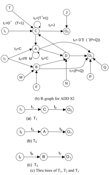
(a) ADD S2
Malaysian Journal of Computer Science, Vol. 23(1), 2010 5
Malaysian Journal of Computer Science, Vol. 23(1), 2010
6 I1
A
I2
B
D C
t1=D¬ (T=1)
t3=C
t2=J O2
O1
M T
N
P J
F t5=(T¬=1)
Q t6=F M
t7=(P<Q) t8=C
t4= D¬ (¬(P<Q))
(b) R-graph for ADD S2
(c) Thru trees of T1, T2 and T3
Fig. 5. R-graph of thru-testable ADD S2.
Example 3: Fig. 5(b) shows the R-graph of the ADD S2. Thru functions t3=C is activated by C. S2 is a thru- testable circuit because there are three thru trees, namely T1, T2 and T3 (shown in Fig. 5(c)) that contain C, B and A which are the vertices in the feedback vertex set (FVS). Moreover, each variable that activates the thru functions in each thru tree is not a vertex in the thru tree. T2 is dependent on T1 because thru function t3 in T2 is activated vertex by C in T1. But thru functions in T1 do not depend on any vertex in T2. There is also no input dependency in S2. Note that node C forms a self loop. Other loop is combination of nodes C, A and D.
3.0 TEST GENERATION MODEL AND PROCEDURE
The test generation model is used to perform a test generation. The thru-extended time expansion model (TTEM) is defined to perform test generation on thru-testable ADD.
3.1 Time Expansion Model
The time expansion model (TEM) is derived from the time expansion graph (TEG) for a given ADD represented by a R-graph. The time expansion graph (TEG) is redefined to facilitate the discussion of test generation model for thru- testable ADD.
Definition 7. Let GR=(V,A,z,t) be an R-graph of an ADD [15] S. Let GT=(VE,AE,F,l) be a directed graph, where VE is a set of vertices, AE is a set of arcs, F is a mapping from VE to a set of integer and l is a mapping from VE to the set of vertices in R. If graph GT satisfies the following five conditions, graph GT is said to be a time-expansion graph (TEG) of GR.
1. C1 (Input/Output preservation): The mapping l is a surjective, i.e., v V, u VE, s.t. v=l(u);
2. C2 (Logic preservation): Let u be a vertex in GT. For any direct predecessor v( pre(l(u))) of l(u) in GR where v≠l(u), there exists a vertex u’ in GT such that l(u’)=v and u’ pre(u). Here, pre(v) denotes the set of direct predecessors of v;
3. C3 (Time consistency): For any arc (u,v) ( AE), there exists an arc (l(u),l(v)) such that F(v)-F(u)=1;
4. C4 (Time uniqueness): For any pair of vertices u,v ( VE), if F(u)=F(v) and if l(u)=l(v), then the vertices u and v are identical, i.e., u=v;
5. C5 (self loop consistency): For any arc (u,v) in GT, if F(v)-F(u)=1 and l(v)=l(u)=z, z is a self loop vertex and the number of predecessor of v is one.
3.2 The Thru-Extended Time Expansion Model (TTEM)
A thru-extended time expansion model (TTEM) of a thru-testable ADD is created using R-graph and the thru trees. TTEM is defined after the TTEG definition.
Definition 8. Let S be a thru-testable ADD [15] with thru trees B and let GR=(V,A,z,t) be the R-graph of S. The thru- extended time expansion graph (TTEG) GT=(VT,AT,F,l) with respect to B is a directed graph that satisfies the following conditions.
1. (Input/Output preservation): The mapping l is surjective, i.e., v V, u VA, s.t. v=l(u);
2. (Logic preservation for fault excitation phase): Let u be a vertex in GR. For any direct predecessor v( pre(u)) of u in GR, there exists vertices y and x in GT such that l(y) = u, l(x) = v, x pre(y) and |pre(y)| = |pre(u)|. Here, pre(y) (resp. pre(u)) denotes the set of direct predecessors of y (resp. u) and |pre(y)| (resp. |pre(u)|) denotes the number of all direct predecessors of y (resp. u);
3. (Thru tree for justification and propagation): Let u be a vertex in a thru tree Ti in B in GR. Let W pre(u) be a set of all direct predecessors of u in Ti. Let tj be a thru function on all incoming arcs of u in Ti and Vtj be a set of vertices that activate tj. For each u in Ti in B in GR, there exists a vertex v in GT which satisfies the following conditions;
a. l(v) = u;
b. For each vertex x in pre(v), the following conditions are satisfied.
i. If there exists a vertex w’ in W such that l(x) = w’ then x pre(z) for any z where l(z) is a vertex included in any other thru tree Tk except Ti and x pre(y) such that l(y) = l(x);
ii. Let Tk be a thru tree that is activated by l(x). If l(x) = l(v), then |pre(v)| = 1 and x pre(z) for any z where l(z) ≠ l(v) and l(z) is a vertex that is not included in thru tree Tk;
iii. If l(x) Vtj, then x pre(z) for any z where l(z) ≠ l(x) and l(z) is a vertex that is not included in thru tree Ti.
|pre(v)| is the number of vertices in pre(v).
4. (Time consistency): For any arc (u, v) ( AT), there exists an arc (l(u), l(v)) such that F(v) − F(u) = 1;
5. (Time uniqueness): For any pair of vertices u, v ( VT), if F(u) = F(v) and if l(u) = l(v), then the vertices u and v are identical, i.e., u = v;
6. (Self loop consistency): Let u be a vertex in GT. Let v ( pre(u)) be a predecessor of u. If |pre(u)| < |pre(l(u))| and l(u) = l(v) = z then |pre(u)| = 1 and z is a self loop vertex;
7. (Input Independency): Let u, v be two vertices in GT. Let pi and pj be a pair of reconvergent paths that start from u and end at v. Let z be a vertex on pi such that u pre(z). Let x be a vertex on pj such that u pre(x). For each pair of paths pi, pj where z≠x, |pre(z)| = |pre(l(z))| and |pre(x)| = |pre(l(x))|;
Definition 9. Let the given thru-testable ADD be denoted by S. The thru-extended time expansion model (TTEM) of S is obtained by the following procedure.
Malaysian Journal of Computer Science, Vol. 23(1), 2010 7
For each pair of consecutive read nodes, replace each vertex in the first slot with the corresponding read node.
Replace each vertex in the second slot with the corresponding write node. Replace each arc with ADD nodes between read node and write node according to the given R-graph.
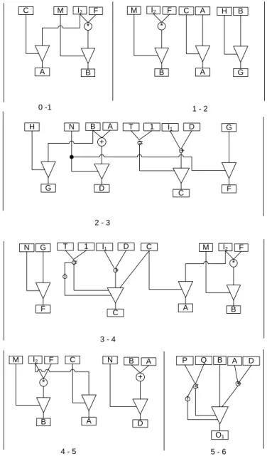
Example 4: Fig. 6 shows the TTEG and TTEM for ADD S2. S2 has no input dependency. Note that node A has a self thru function, t8.
(a) TTEM for ADD S2
Malaysian Journal of Computer Science, Vol. 23(1), 2010 8
A C
A
C A
G
H B
D B
+ N A
F I1 G
C 1 T
=
+ D
A C
D B
+ N A
B I2
* F
M B D
+
O1
P Q
<
!
A B
I2
* F M
B I2
* F M
G H
I1
C 1 T
=
!
C
+ D
F
N G
A B
I2
* F M
0 -1 1 - 2
2 - 3
5 - 6 4 - 5
3 - 4
(b) TTEG of S2
Fig. 6. Test generation model for thru-testable for ADD S2
4.0 DESIGN-FOR-TESTABIITY (DFT) METHOD
We introduce a new DFT method using a high level modeling known as ADD based on testability properties called the thru function. The input to our DFT insertion is a RTL description which consists of non-separable data path and controller. Fig. 8 shows our proposed DFT methodology.
Firstly, the behavioral description is transformed into ADD for thru function extraction. The procedure to extract thru function consists of the following definitions and steps:
Definition 10. Let A be a read node and B be a write node. A connects to data input of an ADN and B connects from the output of the ADN. If data transfer is allowed from path A to B, then A is called on-path input.
Malaysian Journal of Computer Science, Vol. 23(1), 2010 9
Definition 11. Let A and B be read nodes and C be a write node. A and B connect to data input of the ADN and C connects from the output of the ADN. If data transfer is allowed from path A to C then B is called off-path input. Step 1 Identify a set of ADD paths where each path contains one or more of the following:
1.1 any input of addition node 1.2 the first input of subtractions node 1.3 any input of multiplication node 1.4 the first input of division node 1.5 any data input of ADN.
Step 2 Compute the symbolic operations for each line in assignment value part and assignment condition part in terms of variable of read nodes to obtain the operational expression for each line. For example, after the symbolic operation of addition in Fig. 7, the operational expression for line a is (L+M).
Step 3 For each operation node (resp. ADN) on each ADD path, identify the logic, equality, relational and arithmetic operations or any combination of the operations that allows the data transfer from the input (resp. data input) of the operation node (resp.ADN) to its output.
3.1 For an addition node, the condition is the inversion of the operational expression of the off-path input. For example, in the addition node in Fig. 7, data of L is transferred to line a when the off-path input M is 0. In other words, the condition that allows data transfer is M’.
3.2 For a subtraction node, the condition is inversion of the operational expression of the off-path input. For example, in subtraction node in Fig. 7, data of line a is transferred to line b when the off-path input N is 0. In other words, the condition that allows data transfer is N’.
3.3 For a multiplication node, the condition is the operational expression of the off-path input. For example, in the multiplication node in Fig. 7, data of read node N is transferred to line c when the off- path input F is 1. In other words, the condition that allows data transfer is F.
3.4 For a division node, the condition is the operational expression of the off-path input.
3.5 For ADN, the condition is the operational expression of the condition input that corresponds to the on- path input. For example in Fig. 7, data of line b is transferred to write node N when H is 1.
Step 4 Given a path from a read node to a write node, obtain the thru function by ANDing all the conditions that allow data transfer along the path. For example, in Fig. 7, the thru function from L to N (tLN ) = M’.N’.H.
Fig. 7. ADD S3
After extracting the thru functions, ADD is transformed into its R-graph and then identify its thru tree to make thru- testable R-graph. If the R-graph is not thru-testable, we need the DFT insertion by adding minimum number of edges with thru functions into the R-graph so that the R-graph becomes thru-testable. Definition and steps for DFT insertion are taken as follows:
Definition 12. Let A be an input vertex and B be an output vertex. Let C be a vertex which activates a thru function tAB. If data transfer is allowed from A to B through a thru function tAC then C is called an activator.
Step 1 Using the depth first search, start traversing an input vertex to the output vertex without considering whether the outgoing arc has a thru function or not. If the vertex is visited for second time, then the vertex is included in the feedback vertex set (FVS).
Step 2 For each vertex, choose the outgoing arc that has a thru function to continue the traversing. If there is no outgoing arc with thru function then the traversing is stopped.
Malaysian Journal of Computer Science, Vol. 23(1), 2010 10
Step 3 Group each thru function (TF) in the R-graph into sets called TF1, TF2, TF3 and onwards as follows 3.1 Initially include the first thru function into TF1.
3.2 For any i, include the current thru function into TFi if the following conditions i&iii or conditions ii&iii are satisfied.
i. Its input (resp. output) of the current thru function is same with the output (resp. input) of any thru function in TFi.
ii. Its output of the current thru function is same with the output of any thru function in TFi and the activators of the two thru functions are the same.
iii. Its activator is different from any input or output of the thru functions in TFi. 3.3 Create a new TFj (j≠i) if necessary.
Step 4 Check whether all the vertices in feedback vertex set (FVS) are covered by the generated thru function set. If not, group those vertices into FVS’.
Step 5 For each vertex of FVS’, add a new thru function so that the output (resp. input) of the new thru function is the vertex of FVS’ and input (resp. output) of the new thru function is one of the vertex of any existing thru function sets such that the output (resp. input) is not an activator for any thru function in the set.
Step 6 Repeat Step 5 until all vertices in FVS’ are covered by the generated thru function set.
Step 7 If FVS’ is not empty, link the vertices with thru function such that a new thru function is formed.
Step 8 Check whether each thru function set has a primary input and primary output vertex or not. If the set does not have any, one primary input vertex (resp. primary output vertex) in the R-graph is included into the set. If R- graph does not have one, a new vertex is added into the set.
Step 9 Add a new thru function so that the input (resp. output) of the new thru function is the added new input (resp. output) vertex and the output (resp. input) of the new thru function is one of the vertices of any existing thru function sets.
After the DFT insertion, we transform back thru-testable R-graph into thru-testable ADD. We synthesize the thru- testable ADD to gate level netlist. The newly generated gate level netlist has additional gates to realize the new thru functions.
Malaysian Journal of Computer Science, Vol. 23(1), 2010 11
Malaysian Journal of Computer Science, Vol. 23(1), 2010 12 Fig. 8. Our proposed design for testability methodology
5.0 EXPERIMENT SETUP AND RESULTS 5.1 Experiment Setup
The experiment is conducted on ITC’99 benchmark circuits [17] where the behavioral descriptions are given. We extract the information of thru functions from the behavioral descriptions. Tetramax is used to generate tests for the circuits. We show the comparison of the results with partial scan circuits whose minimum feedback set of flip-flops are scanned. Table 1 presents the characteristic of the benchmark circuits. As can be seen in Table 1, #FF represents the number of flip-flops while PI/PO represents the number of inputs/outputs of the circuit. The number of existing thru functions from the behavioral descriptions is described by the column of # thru functions.
Assignment Decision Diagram (ADD)
Extracting thru function
Transforming ADD into its R-graph
Identifying thru tree
DFT insertion
Thru-testable ADD
Synthesis using Design Vision Behavioral description
Gate level netlist
Table 1. Characteristic of the ITC’99 benchmark circuits [17]
IO pins Circuit # Flip-flops Area
PI PO
# Thru functions
ex2 59 901 35 8 8
b03 30 422 6 4 17
b04 66 1179 13 8 40
b07 45 795 3 8 8
b08 21 350 11 4 8
b09 28 396 3 1 1
b10 17 344 13 6 10
b11 31 788 9 6 6
b12 121 2109 7 6 8
b13 51 777 12 10 12
b14 215 10651 34 54 31
b15 417 12810 38 69 69
5.2 Experimental Results
We evaluate the effectiveness of the circuits in terms of fault efficiency, area overhead, test generation time and test application time. Table 2 shows the area overhead where one unit of area corresponds to the size of an inverter. The
#TF added represents the number of newly added thru function and the AO(%) represents the percentage of the area overhead. Table 3 provides the pin overhead, where the PinO denotes the number of the pin overhead while Table 4 provides the fault efficiency where red. denotes redundant faults. Table 5 and Table 6 contain the test generation time and test application time, respectively.
Our method shows that most of the benchmark circuits with thru testability have lower area overhead compared to partial scan designed circuits (Table 2). We added new thru functions at behavioral description before generating the gate level netlist. Therefore, we dealt with less number of components to insert the new thru functions so that the area overhead becomes low. Since the area overhead comes from the newly added thru function, a high area overhead is incurred for circuits b09, b11 and b13 because the existing thru function are less. However, these circuits have a high fault efficiency.
Table 2. Area overhead
Partial Scan [3] Proposed DFT
Circuit Area
#TF added (#TF at bit level)
Area AO(%) #TF added
(#TF at ADD x bitwidth)
Area AO(%)
ex2 901 59 1314 45.84% 49 1143 26.86%
b03 422 30 632 49.76% 12 519 22.96%
b04 1179 66 1641 39.19% 40 1476 25.19%
b07 795 44 1103 38.74% 38 1122 41.13%
b08 350 21 497 42.00% 10 437 24.86%
b09 396 21 543 37.12% 22 557 40.66%
b10 344 17 463 34.59% 8 427 24.13%
b11 788 31 1004 27.41% 38 1065 35.15%
b12 2109 117 2928 38.83% 31 2502 18.63%
b13 777 50 1127 45.05% 56 1146 47.49%
b14 10651 213 12142 14.00% 164 10671 0.18%
b15 12810 414 15708 22.62% 157 13368 4.35%
Malaysian Journal of Computer Science, Vol. 23(1), 2010 13
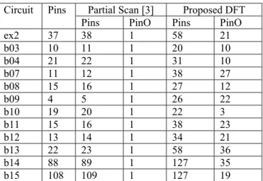
As shown in Table 3, all the benchmark circuits with thru testability have higher pin overhead compared to partial scan designed circuits because in ADD, whenever a new thru function whose input (resp.output) is a new read node corresponding to a primary input (resp.output), this results in a number of new input (resp.output) pins equal to the bitwidth of that read (resp.write) node after synthesis. For example, two new thru functions have been added in the ADD of benchmark circuit b03 which result in one new read node and one new write node. This one new read node is three bits input and one new write node is also three bits output.
Table 3. Pin Overhead
Partial Scan [3] Proposed DFT Circuit Pins
Pins PinO Pins PinO
ex2 37 38 1 58 21
b03 10 11 1 20 10
b04 21 22 1 31 10
b07 11 12 1 38 27
b08 15 16 1 27 12
b09 4 5 1 26 22
b10 19 20 1 22 3
b11 15 16 1 38 23
b12 13 14 1 34 21
b13 22 23 1 58 36
b14 88 89 1 127 35
b15 108 109 1 127 19
Our method shows that most benchmark circuits with the thru testability having a comparable fault efficiency compared to partial scan designed circuits as presented in Table 4. In fact, the fault efficiency of our method is higher than a partial scan designed circuit. For example, the fault efficiency of our method is 92.42% while the fault efficiency of partial scan is 72.03% for benchmark circuit b15.
Table 4. Fault efficiency
Partial Scan [3] Proposed DFT
Circuit FE
Detected Red Total FE Detected Red Total FE
ex2 69.35% 4220 0 4228 99.83% 3778 1 3856 98.22%
b03 69.58% 1703 0 1704 99.94% 1427 0 1446 98.89%
b04 83.39% 4742 36 5040 94.76% 4484 36 4814 94.27%
b07 4.11% 2303 4 3300 69.90% 3612 8 3684 98.37%
b08 92.62% 1352 0 1528 88.48% 1345 0 1358 99.26%
b09 88.18% 1417 0 1421 99.51% 1522 0 1538 99.15%
b10 94.32% 1485 0 1486 99.93% 1464 0 1468 99.83%
b11 81.1% 3393 15 3432 99.30% 3868 13 3916 99.18%
b12 13.75% 7968 2 8962 88.95% 7506 5 8042 93.48%
b13 34.23% 3081 67 3170 99.29% 3265 67 3380 98.79% b14 63.08% 47104 359 48024 98.82% 38783 1983 41530 98.08% b15 4.54% 43012 176 59888 72.03% 49751 56 53892 92.42%
The test generation time in Table 5, shows that most of the benchmark circuits with thru testability have shorter test generation time compared to partial scan designed circuits except for benchmark circuits like b04 and b14. However, the test generation times of these circuits are still shorter or not so longer than original circuit.
Malaysian Journal of Computer Science, Vol. 23(1), 2010 14
Table 5. Test generation time (in seconds)
Circuit Original Partial scan [3] Proposed DFT
ex2 9263.78 108.91 131.93
b03 2229.25 48.13 40.21
b04 1341.99 227.46 547.57
b07 16821.17 11385.33 218.83
b08 326.20 878.07 2.04
b09 516.66 42.80 3.27
b10 514.10 88.91 33.93
b11 4999.26 64.50 44.68
b12 23725.42 13360.22 6474.27
b13 10848.61 113.84 56.25
b14 6540.87 3890.92 6872.46
b15 104084.22 225848.62 95379.67
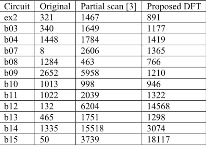
For our method, the test application time is lower than partial scan designed circuits. However, the test application time for benchmark circuits like b08, b12 and b15 are longer than partial scan designed circuits. For benchmark circuit such as b12, although its test application time is longer than partial scan designed circuit but it has shorter test generation time.
Table 6. Test application time (in clock cycles) Circuit Original Partial scan [3] Proposed DFT
ex2 321 1467 891
b03 340 1649 1177
b04 1448 1784 1419
b07 8 2606 1365
b08 1284 463 766
b09 2652 5958 1210
b10 1013 998 946
b11 1022 2039 1322
b12 132 6204 14568
b13 465 1751 1298
b14 1335 15518 3074
b15 50 3739 18117
6. CONCLUSIONS
A new design for testability method has been introduced in this paper based on thru-testability ADD at behavioral description. The DFT method augments a given ADD to become thru-testable ADD. Our method shows that high fault efficiency, lower area overhead, shorter test generation time and shorter test application time in most of the ITC’99 benchmark circuits compared to partial scan designed circuits. Nowadays, the top-down design has become popular, so the DFT at behavioral description is introduced during the early stages of the design flow to improve the testability of the circuits.
Malaysian Journal of Computer Science, Vol. 23(1), 2010 15
ACKNOWLEDGEMENT
This work was supported in part by Malaysian Ministry of Science, Technology and Innovation under ScienceFund Grant (No.01-01-06-SF0473) and in part by Japan Society for promotion of Science (JSPS) under Grants-in-Aid for Scientific Research (B) (No. 20300018).We would like to thank all the members of VeCAD Laboratory in Universiti Teknologi Malaysia, Malaysia for their supporting and valuable help in completing this research.
REFERENCES
[1] H. Fujiwara, “Logic Testing and Design for Testability,” MIT Press, 1985.
[2] M. Abramovici, M. A. Breuer, and A. D. Friedman, “Digital Systems Testing and Testable Design,” IEEE Press, 1990.
[3] K. T. Cheng and V. D. Agrarwal, “A Partial Scan Method for Sequential Circuits with Feedback,” IEEE Transaction Computer, Vol. 39, pp. 544-548, 1990.
[4] R. Gupta and M. A. Breuer, “ The BALLAST Methodology for Structured Partial Scan Design,” IEEE Trans. Computert, vol. 39, no. 4, pp. 538-544, April 1990.
[5] V. Chickermane and S. M. Reddy, “An Optimization Based Approach to the Partial Scan Design Problem,” in Proceeding International Test Conference, pp. 377-386, 1990.
[6]I. Ghosh, and M. Fujita, “Automatic Test Pattern Generation for Functional Register-Transfer Level Circuits using Assignment Decision Diagrams,” IEEE Trans. Computer-Aided Design, Vol. 20. No. 3.pp. 402-415, March 2001. [7] S. Bhattacharya and S. Dey, “H-Scan: A High Level Alternative to Full-Scan Testing with Reduced Area and Test
Application Overheads,” in Proc. IEEE 14th VLSI Test Symposium, pp. 74-80, 1996.
[8] H. Wada, T. Masuzawa, K. K. Saluja and H. Fujiwara, “Design for Strong Testability of RTL Data Paths to Provide Complete Fault Efficiency,” In Proc. Int. Conf.on VLSI Design, 2000.
[9]T. Masuzawa, H. Wada, K. K. Saluja and H. Fujiwara, “A non-scan DFT Method for RTL Data Paths to Achieve Complete Fault Efficiency,” Technical report, Information Science Technical Report: TR98009, Nara Institute of Science and Technology,1998.
[10] S. Ohtake, T. Masuzawa and H. Fujiwara. “A non-scan DFT Method for Controllers to Achieve Complete Fault Efficiency,” In Proc. Asian Test Symp, pp. 204–211. Dec. 1998.
[11] S. Ohtake, H. Wada, T. Masuzawa, and H. Fujiwara. “A non-scan DFT Method at Register-Transfer Level to Achieve Complete Fault Efficiency,” In Proc. Asia and South Pacific Design Automation Conf, pp. 599–604, Jan. 2000.
[12] Chia Yee Ooi and Hideo Fujiwara, “A New Class of Sequential Circuits with Acyclic Test Generation Complexity,” 24th IEEE International Conference on Computer Design, pp. 425-431, October 2006.
[13] Viraphol Chaiyakul and Daniel D. Gajski, “Assignment Decision Diagram for High Level Synthesis,” Technical Report, pp. 5-50, University of California Irvine, October 1992.
[14] V. Chaiyakul, D. D. Gajski, and L. Ramachandran, “High-level transformations for minimizing syntactic variances,” in Proc. Design Automation Conference, pp. 413-418, June 1993.
[15] I.Ghosh and M.Fujita, “ Automatic Test Pattern Generation for Functional Register Transfer Level Circuits using Assignment Decision Diagrams,” IEEE Trans. Computer Aided Design, Vol.20, No.3, pp.402-415, March 2001. [16] Hideo Fujiwara, Chia Yee Ooi and Yuki Shimizu, “Enhancement of Test Environment for Assignment Decision
Diagrams,” IEEE Workshop on RTL and High Level Testing, pp.45-50, 2008. [17] http://www.cerc.utexas.edu/itc99-benchmarks/bench.html.
Malaysian Journal of Computer Science, Vol. 23(1), 2010 16
Malaysian Journal of Computer Science, Vol. 23(1), 2010 17
BIOGRAPHY
Norlina Binti Paraman received the B.E degree in Computer Engineering and M.E degree Electronic and Telecommunication Engineering from Universiti Teknologi Malaysia, Malaysia in 2003 and 2006 respectively. She is currently doing her Ph.D study in Universiti Teknologi Malaysia, Malaysia.
Chia Yee Ooi received the B.E and M.E degrees in Electrical Engineering from Universiti Teknologi Malaysia, Malaysia in 2001 and 2003, respectively, and Ph.D in Computer Design and Test from Nara Institute of Science and Technology, Japan in 2006. She is currently a senior lecturer in Universiti Teknologi Malaysia, Malaysia. Her research interests include VLSI design and testing. She is also a member of IEEE.
Ahmad Zuri Bin Sha’ameri received the B.E degree in Electrical Engineering from University Missouri, USA in 1984, and M.E and Ph.D degrees in Electrical Engineering from Universiti Teknologi Malaysia, Malaysia in 1991 and 2000, respectively. He is currently an Associate Professor in Universiti Teknologi Malaysia, Malaysia. His research interests include signal theory, signal analysis and classification, mobile and cellular radio communications, biomedical signal processing, machine condition monitoring and information security. He is a member of IEEE, member of Digital Signal Processing and Communication Society and member of Eta Kappa Nu-Electrical Engineering Honor Society.
Hideo Fujiwara received the B.E, M.E and Ph.D degrees in electronic engineering from Osaka University, Osaka, Japan, in 1969, 1971, and 1974, respectively. He is currently a Professor at the Graduated School of Information Science, Nara Institute of Science and Technology, Nara, Japan. His research interests are logic design, digital systems design and test, VLSI CAD and fault tolerant computing, including high level/logic synthesis for testability, test synthesis, design for testability, built in self test, test pattern generation, parallel processing and computational complexity. He is the author of Logic Testing and Design for Testability (MIT Press, 1985). He also a fellow of the IEEE, a Golden Core member of the IEEE Computer Society, a fellow of the IEICE (the Institute of Electronics, Information and Communication Engineers of Japan) and a fellow of the Information Processing Society of Japan.


![Table 1. Characteristic of the ITC’99 benchmark circuits [17]](https://thumb-ap.123doks.com/thumbv2/123deta/5754011.27241/13.918.280.660.150.422/table-characteristic-itc-benchmark-circuits.webp)