Extended Compatibilities for Scan Tree Construction
Zhiqiang You Michiko Inoue Hideo Fujiwara
Nara Institute of Science and Technology, Ikoma, Nara 630-0192, Japan
{you-z, kounoe, fujiwara}@is.naist.jp
Abstract
Scan tree techniques reduce test application time significantly by shifting test values into (out from) the compatible flip-flops simultaneously. This paper proposes a novel scan tree architecture for test application time and test power reduction. In this proposed method, the compatibility is extended by employing NOT gates and XOR gates. Experimental results show that our approach is more effective to achieve short test application time and low test power compared with the conventional scan tree design.
Key words:
design for testability, full scan testing, scan tree, low power testing1. Introduction
With the transistor counts exponential increase, scan-based designs are widely employed to reduce test generation time. Full scan-based design is one of the most important design for testability (DFT) methodologies in very large scale integration (VLSI) circuits and in system-on-hip (SoC) cores. In this DFT methodology, all flip-flops are enhanced to scan cells, and test application time depends on the length of the longest scan chain. Though full scan design reduces test generation complexity drastically, the test cost is very high that increases the cost of automatic test equipment (ATE).
There huge number techniques have investigated low cost test. Some methodologies [1-4] explore new scan architectures. The method in [1] effectively reduces test data volume and test application time for designs with multiple scan chains using a reconfigurable switch to apply tests from a limited number of external inputs to a large number of internal scan chains. VirtualScan technology is proposed in [2] to reduce test cost based on the idea of reducing the longest scan chain length in a full-scan circuit. The technique in [3] reduces test data volume and test application time drastically by employing the CircularScan architecture that uses the captured response for the next vector by replacing only necessary bits.
However, in these methods, to achieve short test application time there are too many transitions in the circuit under test (CUT). The power dissipation is quite high. If the test power dissipation exceeds the designed power constraint, it can give rise to severe hazards in circuit reliability or can provoke instant circuit damage
[4]. Hence, it is more important to achieve low test cost with low test power.
Various techniques have been proposed to reduce switching activity during test to reduce power. The methodologies in [5-8] employ test vector or scan cell reordering technique where test vectors in a test set or scan cells for a test set are reordered for minimal power consumption. The methodologies in [9,10] also explore the correlation between consecutive test patterns by filling each don’t care bit in the test cubes with appropriate value 0 or 1. There are some methods [11- 15] that reduce power consumption by using scan chain disabling technique. In methods of [11-14], only one scan chain at the same time is activated during scan shifting. The power during scan shifting is reduced to 1/N, where N is the number of scan chains. [15] reduces both peak power and average power dissipation by simultaneously activating only one scan chain during both shift and cycles. However, these methodologies did not consider test application time or test data volume reduction.
Recently, scan tree techniques [16-20] have been proposed to reduce test application time and test power. In these techniques, scan cells are constructed into a tree structure. The length of the longest scan chain is reduced. During scan operation, test data are shifted into the scan tree via one scan cell at the root. The scan cells in the same level have the same shifted test data. Therefore, to keep fault coverage, the scan cells should be compatible for all the test vectors.
As the first technique concerning scan tree, [16] constructs a scan tree and minimizes its height by test vector modification. [17] extends the methodology in [16] into multiple scan chain cases. [18] improves the solution of scan tree technique by adopting a folding mode to enhance the parallelism. In [20], test application time and test data volume are reduced drastically by a dynamic reconfiguration between the scan chain mode and the single scan mode.
In this paper, we extend the concept of compatibility for scan tree techniques. And we propose a novel scan tree architecture to achieve short test application time and low test power. Notice that, the method in [20] adapts to our methodology. If we apply this technique to our method, the test application time can be reduced more and our technique is applicable to update test vectors for the CUT.
This paper is organized as follows. Section 2 introduces some basic concepts about scan tree techniques. Section 3 describes our proposed scan tree architecture with extended compatibilities. Section 4 gives the algorithm to construct a scan tree. Section 5
11th IEEE European Test Symposium, pp. 13-18, May 2006.
reports on some experimental results for our proposed method. Section 6 concludes with a brief summary.
2. Scan Tree Architecture
Scan tree architectures group the compatible scan flip-flops in the same level so that the scan cells can receive the same test values for all the test vectors. These technologies shorten the length of the scan chain, and hence, reduce test application time and test data volume. Scan tree methodologies are more effective for the test set with don’t care values. Let X denote a don’t care value.
Definition 1. For a test set T, scan cells ffi and ffj are normal-compatible, if for any test cube cm in T, vi,m =
vj,m, vi,m = X or vj,m = X, where vi,m is the value of scan cell i of test cube cm.
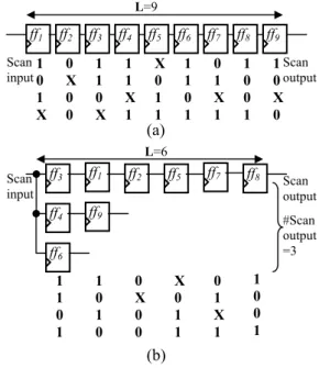
Fig. 1.(a). shows an example of a single scan chain with 9 scan cells and a test set. According the compatibility of scan cells, ff3, ff4 and ff6, ff1 and ff9 are grouped in the same level respectively. ff2, ff5, ff7, ff8
are not compatible with any other scan cells. After the scan cells are grouped, some don’t care bits corresponding to the scan cells may be specified. The scan tree architecture and its test set are shown in Fig. 1.(b). The X in ff1 is specified to 0 since value of the corresponding bit in its compatible scan cell, ff9 is 0. The length of the longest scan chain is reduced from 9 to 6. Therefore, both test application time and test data volume are reduced by 1/3. The number of scan outputs is 3. We can use an embedded MISR to analyze the test responses.
3. Proposed Scan Tree Architecture
In this section, we will describe the proposed scan tree architecture.
3.1 Compatibility Extension
We give a basic definition and extend a concept of normal-compatibility by employing NOT gates and XOR gates in this subsection.
Definition 2. A scan cells is in the i-th level of a scan tree, if its test data can be shifted into it from the scan input through i scan shift cycles.
Definition 3. For a test set T, scan cells ffi and ffj are NOT-compatible, if for any test cube cm in T, vi,m≠ vj,m, vi,m = X or vj,m = X, where vi,m is the value of scan cell i of test cube cm.
Definition 4. For a test set T, scan cells ffi and ffj are XOR-compatible for ffk, if for any test cube cm in T, vi,m⊕ vj,m= vk,m, vi,m = X, vj,m = X or vk,m = X, where vi,m is the value of scan cell i of test cube cm.
Using both NOT gate and XOR gate, the NXOR- compatibility is defined as follows.
Definition 5. For a test set T, scan cells ffi and ffj are NXOR-compatible for ffk, if for any test cube cm in T, vi,m⊕ NOT(vj,m)= vk,m, vi,m = X, vj,m = X or vk,m = X, where vi,m is the value of scan cell i of test cube cm.
L=9
To simplify the notation, we will use ffi = NOT (ffj), ffk = ffi ⊕ ffj, ffk = ffi ⊕ NOT(ffj) to represent the above compatibilities respectively.
3.2 Proposed Architecture
The scan cells that are normal- or NOT- compatible with each other can be grouped into a clique. We describe three theorems that are the base to construct a scan tree of the extended compatibilities as follows.
Theorem 1. The scan cells in a clique can be grouped into the same level.
Theorem 2. If there exist two cliques Ci and Cj, and scan cells ffk, ffm are XOR- or NXOR-compatible with any scan cell in Ci for any scan cell in Cj respectively, the following statement is true. The scan cells ffk, ffm are normal- or NOT-compatible if and only if it does not cause any conflict when specifying don’t care bits corresponding to the scan cells in Ci and Cj.
We can find the maximal clique Ck where any scan cell is XOR- or NXOR-compatible with any scan cell in Ci for any scan cell in Cj. To simplify, we call this case as Ck is XOR-compatible with Ci for Cj. Theorem 3. If there exist three cliques Ci, Cj and Ck, and any scan cell in Ck are XOR- or NXOR-compatible with any scan cell in Ci for any scan cell in Cj, the scan cells of Ck can be grouped in the same level as the higher level between Ci and Cj in a scan tree.
Theorem 4. Among the cliques in level l1, there exists only one clique Cl1,0 so that for any other clique Cl1,m1
(m1>0) there exist a clique Cl2,m2 (l2<l1, m2≥0) Cl1,m1 is XOR-compatible with Cl1,0 for Cl2,m2.
We call the clique Cl1,0 as primary clique in level l1.
The scan tree is constructed as following. First, we connect the scan cells in the primary cliques between the neighboring levels. Secondly, we connect ff1 ff2 ff3 ff4 ff5 ff6 ff7 ff8 ff9
1 0 X 0 0
1 1 0 X
1 1 X 1
X 0 1 1
1 1 0 1
0 1 X 1
1 0 0 1
1 0 X 0
Scan output 0
Scan input 1 X
(a) ff1 ff2
ff3
ff4
ff5
ff6
ff7 ff8 L=6
ff9 Scan
input
Scan output
#Scan output
=3 1 0 0 1 1
1 0 1
1 0 1 0
0 X 0 0
X 0 1 1
0 1 X 1 Fig. 1. Scan tree architecture
(b)
the scan cells in other cliques according to their XOR- or NXOR-compatibilities. Notice that, to keep fault coverage, in the second step, we cannot remove the scan output of step 1as one input of an XOR gate. And all the scan cells are not in the primary cliques have scan output themselves.
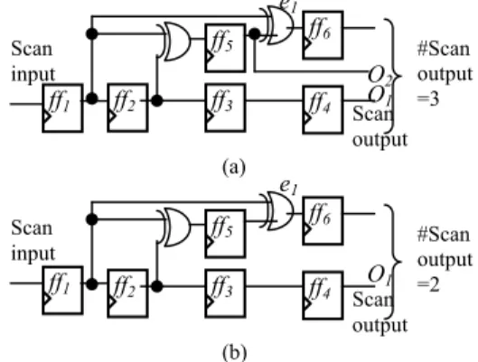
Fig. 2. gives a scan tree architecture with the extended compatibilities for the scan cells and the test set shown in Fig. 1.(a). Since ff7 is NOT-compatible with ff1 and ff9, they are grouped into the second level. ff2 and ff5 are grouped into a clique because they are NOT-compatible. ff2, ff8 and ff5, ff8 are XOR-compatible for any scan cell in the first level. Therefore, we can put ff2, ff5, ff8 into the third level. The construct scan tree is shown in Fig. 2. The length of the longest scan chain is reduced to 3. Test application time and test data volume are reduced by 2/3. The added hardware is one NOT gate and one XOR gate. The number of scan outputs is 4, that is, a little higher than the scan tree architecture in Fig. 1.(b)..
3.3 The Number of Scan Outputs Reduction The higher number of scan outputs may cause higher hardware overhead to analyze the test responses of scan cells. To reduce the number of scan outputs without affecting fault coverage, we compact scan outputs according to the following three rules. In the following rules, to simplify we show and explain them to employ scan cells. It also effect by change the term from scan cell to clique.
Rule 1. If a scan cell ffi is XOR- or NXOR- compatible with scan cell ffj for the scan cell ffk of the first level, and there exists one scan output Ol in the preceding level, the scan output can be connected to one input of the XOR gate to reduce one scan output. This is because the test responses of scan cells along the scan path from scan input to the scan output Ol
cannot be masked when do scan operations.
For example, in Fig. 2, ff8 is such scan cell. There
is a scan output at the second level. We utilize this line to propagate test data for ff8. The result is shown in Fig. 3.
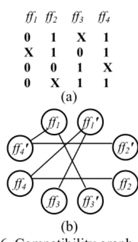
Rule 2. If scan cells ffi1, ffi2 are XOR- or NXOR- compatible with scan cells ffj1, ffj2 for the scan cells ffk1, ffk2 respectively, and ffk1, ffj1 are direct predecessors of ffk2, ffj2 respectively, the scan cell ffi2 can be a direct successor of ffi1. The reason is as follows. When performing scan operation, the test data of ffj2, ffk2 are propagated from ffj1, ffk1. Just before the last shift cycle, ffj1, ffk1 store the test data of ffj2, ffk2. Because ffi1 = ffj1 ⊕ ffk1 ffi1 stores the test data of ffj2 ⊕ ffk2. Therefore, ffi2 can be the next scan cell of ffi1 along the scan tree.
For example, in Fig. 4.(a), scan cells ff4, ff5 have the same situation with ffi1 and ffi2. ff4 = ff1⊕ ff2, while ff5 = ff2 ⊕ ff3; ff1 and ff2 are the scan cells just before ff2
and ff3 in the scan tree respectively. After removing a scan output, the result is shown in Fig. 4.(b).
Rule 3. If a scan cell ffj has more than one outputs where one is a scan output Ol, and if there exists one of their direct successors of gates or scan cells eh where the test response of all the direct
predecessors of scan cells except ffj can be propagated a scan output without eh, the scan output Ol can be removed. This is because the test response of ffj can be propagated through eh to a scan output.
For example, as shown in Fig. 5.(a), ff5 has two outputs, and one of the outputs O2 is a scan output. e1 is its a direct successor. There is one predecessor ff1 of e1
except ff5. The test response of ff1 can be to a scan ff1 ff2
ff3
ff4
ff5
ff6 ff7
ff8
ff9 Scan
input
Scan output L=3
#Scan output
=3
Fig. 3. Reducing the number of scan output using Rule 1.
ff1 ff2 ff3
ff4
ff5
Scan input
#Scan output Scan =3 output (a)
ff1 ff2 ff3
ff4 ff5
Scan input
#Scan output Scan =2 output (b)
Fig. 4. Reducing the number of scan output using Rule 2.
ff2 ff3 ff4
ff5 ff6 Scan
input
#Scan output Scan =3 output (a)
#Scan output Scan =2 output (b)
Fig. 5. Reducing the number of scan output using Rule 3
ff2 ff3 ff4
ff5 ff6 Scan
input ff1 ff1
O2
e1
e1
O1
O1
ff1 ff2
ff3
ff4
ff5
ff6 ff7
ff8
ff9 L=3 Scan
input
Scan output
#Scan output
=4
Fig. 2. Scan tree architecture with the extended compatibilities
output O2. Fig. 5.(b). shows the scan tree after the reduction.
In the following approach, we realize these rules to reduce the number of scan outputs. There are still some rooms to reduce more. For instance, if we consider the structure of a circuit, which different scan paths may share one scan output if the scan cells in the same level from output cannot capture error of a fault, the number of scan outputs can be reduced. Data compaction techniques [21], also give solutions to reduce the number of scan outputs. In this paper, we do not deal with these cases.
3.4 Average Power Reduction
Our method probably reduces the transitions between the neighboring levels of a scan tree to employed NOT gates and XOR gates. Therefore, the proposed architecture adapts to reduce average power. The results shown in the experimental results part will evaluate the efficiency.
4. Optimal Algorithm to Construct a Scan
Tree
In this section, we describe the proposed approach to find an optimal scan tree for full scan design with one scan input and a given test set.
4.1 Compatibility Graph
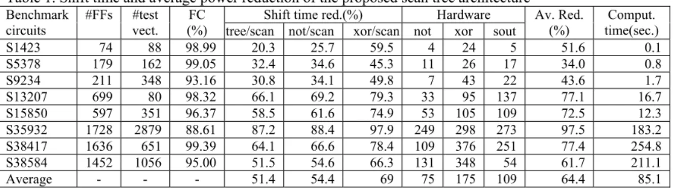
A compatibility graph represents the relations of scan cells. To explain the NOT-compatibility, a scan cell is represented by two nodes. One node represents the scan cell itself. The other node stands for its complement values. An edge exists between two nodes if the corresponding scan cells are normal-compatible. For example, for the given test cubes in Fig. 6.(a), the compatibility graph can be constructed as Fig. 6.(b).
4.2 Overview
The aim of this algorithm is to find the minimum number of levels of cliques. Since the problem is NP- hard, we use a heuristic algorithm shown in Fig. 7. We first construct the compatibility graph G with normal-
and NOT-compatibilities (line 1). In this algorithm, we reduce a clique into a node. To distinguish the original nodes, in the rest we call the node as a clique node while the original nodes are named as scan cell nodes. During the scan tree construction process (lines 3-7), we find a clique set i of G such that the number of scan cells that are in all the cliques of clique set i are maximized (line 4, algorithm FINDCLIQUES shown in section 4.3). Algorithm FINDCLIQUES also performs to specify don’t care bits of a test set for the compatible scan cells, to update the graph G, and to generate the i- th level of the scan tree. The algorithm ends until graph G is empty.
Scan tree construction algorithm for extended compatibilities
1. Construct the compatibility graph G; 2. i=1;
3. Repeat {
4. FINDCLIQUES i of G; 7. i++;
8. }
9. Until G is empty;
Fig. 7. Scan tree construction algorithm 4.3 Finding a Maximal Clique Set
In this subsection, we will give an algorithm to find a maximal clique set of G. This problem is high complexity. We employ a heuristic algorithm, shown in Fig. 8, where we first find a maximal clique Ci,0 (line 1). Secondly, we specify some don’t care bits of test values corresponding to the scan cells represented by the nodes in the clique Ci,0 (line 2). Thirdly, we record a node pi,0 to present the clique (line 3). Fourthly, we update graph G by removing all the scan cell nodes of the clique and their complement nodes (line 4). After that, for every clique node pj,k in G, where j<i, we find the maximal clique Ci,m where the nodes are XOR- or NXOR-compatible with p i,0 for pj,k. Then, Specify some don’t care bits of the test set corresponding to the nodes in Ci,m, Ci,0 and Cj,k considering not only the compatibilities of inside the cliques Ci,m, but also the relation of Ci,m, Ci,0 and Cj,k. Here, the values of some bit of Ci,m, Ci,0 and Cj,k may be “partially” specified. For example, if one bit of the values of three XOR compatible nodes in a test cube are X, X, and 0 respectively. The relation is not enough to specify the don’t care bit. Nevertheless, the first two Xs should have the same specified values when applying the test to a CUT. We keep such information for the further specification. We record a node pi,m to present the clique And graph G is updated in the same way as the beginning of the paragraph. According to theorem 3, all the cliques in a clique set can be grouped in the same level. Next, the i-th level of the scan tree is generated by connecting the scan cells in the (i-1)-th level (line 13). In this step, the connection between the scan cells in the neighboring levels are considered to reduce hardware overhead by sharing NOT gates, XOR gates ff1 ff2 ff3
0 X 0 0
1 1 0 X
X 0 1 1
1 1 X 1 (a)
ff1' ff1
Fig. 6. Compatibility graph ff2' ff4'
(b) ff3
ff4
ff4 ff2
ff3'
or the rules of scan output reduction. Finally, the clique set i and the i-th level of the scan tree are returned (line 14).
Notice that, in our method we group the large clique set in the low level of a scan tree, which efficiently explores the compatibilities and reduce hardware overhead.
5. Experimental Results
We have conducted experiments on full scan version of ISCAS’89 benchmark circuits in C language on a Pentium III Mobile 800MHz with 256 MB RAM. In the experiments, we use the ATPG tool "TestGen" of Synopsys to generate test cubes and perform fault simulation.
Table 1 shows the results of ISCAS’89 benchmark circuits. The first four columns give the circuit’s names, the number of scan cells, the number of test vectors and fault coverage. The following three columns draw the percentages of shift time or test data reduction between the scan tree technique with normal- compatibility, the scan tree technique with normal- and NOT-compatibilities, the proposed method and that of the single scan chain respectively. The added number of NOT gates, XOR gates and scan outputs are shown in the next three columns. The column “Av. Red. (%)” reports the percentages of average power reduction of the proposed method compared with full scan design
with one scan chain. The last column displays the computation time to construct a scan tree and to obtain its test vectors in seconds.
Algorithm FINDCLIQUES: Finding the maximal clique set i
1. Find a maximal clique Ci,0;
2. Specify some don’t care bits of the test set corresponding to the nodes in the clique; 3. Record a node pi,0 to present the clique; 4. Remove the nodes in Ci,0 and their
complement nodes; 5. m=1;
6. For every clique node pj,k (except p i,0) { 7. If existing, find the maximal clique Ci,m
where the nodes are XOR- or NXOR- compatible with p i,0 for pj,k;
8. Specify some don’t care bits of the test set corresponding to the nodes in Ci,m, Ci,0and Cj,k;
9. Record a node p i,m to present the clique; 10. Remove the nodes in Ci,m and their
complement nodes; 11. m++;
12. }
13. Generate the i-th level of the scan tree by connecting the scan cells in the (i-1)-th level;
14. Return the clique set i and the i-th level of the scan tree;
In this experiment, we estimate shift time reduction by the longest scan path reduction. As some published methods do, we use the technique in [9] to estimate test power.
As shown in Table 1, the shift time reduction for the scan tree technique with normal-compatibility is 51.2% in average, and up to 87.2%. The method employing one extended compatibility, NOT- compatibility can achieve a little better results. The reduction is 54.4% in average, and up to 88.4%. Our proposed method is more effective to reduce test application time and test data. The reduction is 68.9% in average, and up to 97.9%. The hardware overhead is not very high. The computation time is short even for the largest circuits.
Notice that, the average power dissipation also can be reduced in the architecture to reduce test application time. The percentage of the reduction is 64.4 in average. The proposed method also adapts to reduce test power.
6. Conclusions
This paper proposed a novel scan tree architecture for test application time, test data volume and test power reduction. In this architecture, the compatibility is extended to NOT-, XOR-, NXOR- and normal-compatibilities by employing NOT gates and XOR gates. Experimental results show that our approach is more effective to achieve short test application time, low test data volume compared with the conventional scan tree design. The average power is also reduced drastically.
Fig. 8. Finding the maximal clique set
The scan chain routing problem may occur if some scan cells that have far distances are connected together. Future work will investigate the layout impact to our methodology.
Acknowledgments
This work was supported in part by Japan Society for the Promotion of Science (JSPS) under Grants-in- Aid for Scientific Research B(2) (No. 15300018).
The authors wish to thank Drs. Satoshi Ohtake, Tomokazu Yoneda and Thomas Clouqueur of Nara Institute of Science and Technology, for their valuable comments. Thanks are also due to the members of Fujiwara laboratory.
References
[1] H. Tang, S. M. Reddy and I. Pomeranz, “On reducing test data volume and test application time for multiple scan chain designs,” In Proc. IEEE International Test Conference, pp. 1079-1088, 2003.
[2] L.-T. Wang, X. Wen, H. Furukawa, F.-S. Hsu, S.-H. Lin, S.-W. Tsai, K. S. Abdel-Hafez and S. Wu, “VirtualScan: a new compressed scan Technology for test cost
reduction”, In Proc. IEEE International Test Conference, pp. 916-925, 2004.
[3] B. Arsian and A. Orailoglu, “CircularScan: a scan architecture for test cost reduction”, In Proc. Of the IEEE Design, Automation and Test in Europe Conference, pp. 1290-1295, 2004.
[4] Patrick Girard, “Survey of Low-Power Testing of VLSI Circuits,” IEEE Design & Test of Computers, vol. 19, no. 3, pp82-92, 2002.
[5] S. Chakravarty and V. Dabholkar, “Two techniques for minimizing power dissipation in scan circuits during test application,” In Proc. IEEE Asian Test Symposium, pp. 324-329, 1994.
[6] V. Dabholkar, S. Chakravarty, I. Pomeranz and S.M. Reddy, “Techniques for minimizing power dissipation in scan and combinational circuits during test application,” IEEE trans. On Computer-Aided Design of Integrated Circuits and Systems, Vol. 17, No. 12, pp. 1325-1333, 1998.
[7] P. Flores. J. Costa, H. Neto, J. Monterio and J. Marq1ues-Silva, “Assignment and reordering of incompletely specified pattern sequences targeting minimum power dissipation,” Proc. Of International Conference on VLSI Design, pp. 37-41, 1999.
[8] Y. Bonhomme, P. Girard, L. Guiller, C. Landrault and S. Pravossoudovitch, “Efficient scan chain design for power minimization during scan testing under routing constraint,” In Proc. IEEE International Test Conference, pp. 488-493, 2003.
[9] R. Sankaralingam, R. R. Oruganti and N. A. Touba,
“Static compaction techniques to control scan vector power dissipation,” In Proc. IEEE VLSI Test Symposium, pp. 35-40, 2000.
[10] K. M. Butler, J. Saxena, T. Fryars, G. Hetherington, A. Jain and J. Lewis, “Minimizing power consumption in scan testing: pattern generation and DFT techniques,” In Proc. IEEE International Test Conference, pp. 355-364, 2004.
[11] L.Whetsel, “Adapting scan architectures for low power operation,” In Proc. IEEE International Test Conference, pp. 863-872, 2000.
[12] J. Saxena, K. M. Butler and L. Whetsel, “An analysis of power reduction techniques in scan testing,” In Proc. IEEE International Test Conference, pp. 670-677, 2001. [13] Y. Bonhomme, P. Girard, L. Guiller C. Landrault and S.
Pravossoudovitch, “A gated clock scheme for low power scan testing of logic Ics or embedded cores,” In Proc. IEEE Asian Test Symposium, pp. 253-258, 2001. [14] B. B. Bhattacharya, S. C. Seth and S. Zhang, “Double-
tree scan: a novel low-power scan-path architecture,” In Proc. IEEE International Test Conference, pp. 471-479, 2003.
[15] Z. You, T. Iwagaki, M. Inoue and H. Fujiwara, “A low power deterministic test using scan chain disable technique,” IEEE 6th Workshop on RTL and High Level Testing, pp.184-191, July 2005.
[16] K. Miyase and S. Kajihara, “Optimal Scan Tree Construction with Test Vector Modification for Test Compression,” In Proc. IEEE Asian Test Symposium, pp. 136-141, 2003.
[17] K. Miyase, S. Kajihara and S. M. Reddy, “Multiple Scan Tree Design with Test Vector Modification,” In Proc. IEEE Asian Test Symposium, pp. 76-81, 2004.
[18] H. Yotsuyanagi, T. Kuchii, S. Nishikawa, M. Hashizume, K. Kinoshita, “Reduce Scan Shifts using Folding Scan Trees,” In Proc. IEEE Asian Test Symposium, pp. 6-11, 2003.
[19] D. Xiang, S. Gu, J.G. Sun and Y. Wu, “A Cost-Effective Scan Architecture for Scan Testing with Non-scan Test power and Test application Cost,” In Proc. Design Automation Conference, pp. 744-747, 2003.
[20] Y. Bonhomme, T. Yoneda, H. Fujiwara and P. Girard,
“An Efficient Scan Tree Design for Test Time Reduction,” In Proc. IEEE European Test Symposium, pp. 174-179, 2004.
[21] T. Clouqueur, K. Zarrineh, K. K. Saluja and Hideo Fujiwara, “Design and Analysis of Multiple Weight Linear Compactors of Responses Containing Unknown Values,” In Proc. IEEE International Test Conference, 2005.
Table 1. Shift time and average power reduction of the proposed scan tree architecture Shift time red.(%) Hardware Benchmark
circuits
#FFs #test vect.
FC
(%) tree/scan not/scan xor/scan not xor sout
Av. Red. (%)
Comput. time(sec.)
S1423 74 88 98.99 20.3 25.7 59.5 4 24 5 51.6 0.1
S5378 179 162 99.05 32.4 34.6 45.3 11 26 17 34.0 0.8
S9234 211 348 93.16 30.8 34.1 49.8 7 43 22 43.6 1.7
S13207 699 80 98.32 66.1 69.2 79.3 33 95 137 77.1 16.7
S15850 597 351 96.37 58.5 61.6 74.9 53 105 109 72.5 12.3
S35932 1728 2879 88.61 87.2 88.4 97.9 249 298 273 97.5 183.2
S38417 1636 651 99.39 64.1 66.6 78.4 109 376 251 77.4 254.8
S38584 1452 1056 95.00 51.5 54.6 66.3 131 348 54 61.7 211.1
Average - - - 51.4 54.4 69 75 175 109 64.4 85.1