Kenichi HATASAKO†a),Member, Tetsuya NITTA†, Masami HANE††,andShigeto MAEGAWA†,Nonmembers
SUMMARY This paper discusses Mixed Signal LSI technology with embedded power transistors. Trends in Mixed Signal LSI technology are explained at first. Mixed signal LSI technology has proceeded with the help of fine fabrication technology and SOI technology. The BEOL transistor is a new development, which uses InGaZnO (IGZO) as its TFT channel material. The BEOL transistor is one future device which enables 3D IC and chip shrinking technology.
key words: Mixed Signal LSI, BiC-DMOS, analog, power IC, InGaZnO (IGZO)
1. Introduction
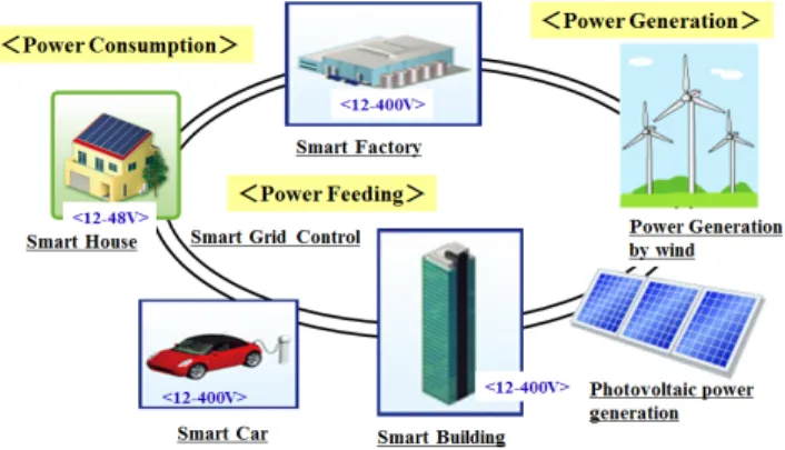
The electronic apparatus and the electrical components need to be high efficiency energy saving types because of en- vironmental problems and energy supply problems. Fig- ure 1 shows a “smart society” which realizes high efficiency and energy saving in electric generation, power feeding and power consumption to achieve a low carbon society. As power devices and power LSI are important tools for the cre- ation of a high efficiency energy saving society, power de- vices and power LSI are being developed to have a more and more important role. This paper presents Mixed Signal LSI technology, which can process digital signals, analog sig- nals, and power management with embedded power devices.
The Mixed Signal LSI uses BiC-DMOS devices, which have CMOS transistors, Bipolar transistors, and DMOS transis- tors. Mixed Signal LSI technology is widely used for power management, motor drivers, automotive LSIs, etc. by using the advantages of BiC-DMOS devices.
Trends in Mixed Signal LSI technology are described first. Mixed Signal LSI has progressed rapidly from dis- crete devices to integrated LSI and has become “true System LSI”. Its progress is supported by improvement in device performance and reduction in device size. These improve- ments have been made mainly through the fine fabrication technology and high voltage device technology.
In addition, BEOL transistors made by wideband gap semiconductor InGaZnO (IGZO) are presented. BEOL tran- sistors are formed in the wiring layer, which can realize high voltage devices and can isolate high voltage devices from a silicon substrate. Though BEOL transistor technology is
Manuscript received November 27, 2013.
Manuscript revised December 26, 2013.
†The authors are with Mixed Signal Device Tech. Dept., Rene- sas Electronics Corp., Itami-shi, 664-0005 Japan.
††The author is with Advanced LSI Devices Research, Renesas Electronics Corp., Sagamihara-shi, 252-5298 Japan.
a) E-mail: [email protected] DOI: 10.1587/transele.E97.C.238
Fig. 1 Low carbon smart society. Bracketed voltage indicates voltage supplied to BiC-DMOS device.
still under development, it is expected to realize future BiC- DMOS devices.
BiC-DMOS devices have a buried layer and an epitax- ial growth layer with the advantages of each. Though buried layers and epitaxial layers are not necessarily formed for low voltage application, low noise application, etc., this paper shows the device structure with a buried layer and an epi- taxial growth layer.
2. Trends in Mixed Signal LSI with Embedded Power Devices
2.1 Trends in Mixed Signal LSI with Embedded Power Devices
Figure 2 shows trends in Mixed Signal LSI with embedded power devices. These trends are based on mass production basis and development is thought to be about 5 years ahead of that are shown in Fig. 2. In Fig. 2, we can see that ana- log, digital and power IC were originally discrete technolo- gies. Analog IC and digital IC began to be put together in the same chip around 1990. After this, as device size be- came smaller with the support of fine fabrication technology, the integration of different types of device accelerated. At present, logic LSI, analog LSI, power LSI, RAM, ROM and CPU are all integrated in the same chip [1]–[3]. One chip can process every signal and perform every system function from the input signal to the output signal. It has become a
“true system LSI”.
The reasons why the integration of different types of device has proceeded so rapidly are as follows:
Copyright c2014 The Institute of Electronics, Information and Communication Engineers
Fig. 2 Trends in Mixed Signal LSI with embedded power devices. These trends are based on mass production basis.
Fig. 3 The main stream structure for mixed signal LSI.
(1) Reduction in number of parts.
(2) Reduction in size.
(3) Integration of IC/LSI functions (communication, mem- ory, etc.).
(4) Simplification in hardware design.
(5) Value-added software control.
These are the requirements from various systems, such as mobile equipment, automotive, etc. Mixed Signal LSI tech- nology has advanced in response to these requirements [4].
Another method of integrating different types of de- vices is the SIP (System in Package) solution. The SIP so- lution has unique advantages. The main advantages are:
(1) Value addition without chip change.
(2) Product development is easier than one chip solution (SOC).
Therefore, it is suitable for a small amount of LSI and quick TAT (Turn Around Time) LSI. SIP and SOC solutions will continue to be developed through complementary use.
Figure 3 shows the main stream structure for Mixed Signal LSI. At present, SOC and SIP are the representa- tive structures for Mixed Signal LSI. SOC and SIP en- able mixed signal LSI to have more integration, smaller
Fig. 4 BiC-DMOS device structure.
Fig. 5 HVCMOS device structure.
chip size/package, higher speed, lower power consump- tion, etc. However, these technologies have a tendency to make the product more expensive for low end LSI be- cause new production process for large integration SOC- chips/SIP-packages have many steps and this increases the fabrication cost. Therefore, we propose “SOC+InGaZnO (IGZO)” style integration for low end LSI. The details of which are reviewed after the next section.
2.2 Mixed Signal LSI Structures with Embedded Power Transistors
Figure 4 shows a BiC-DMOS device structure, which is ex- clusively used for mixed signal LSI [5]. The main device is composed of CMOS (NMOS/PMOS), Bipolar (NPN/PNP), DMOS, HVPMOS, resistor, capacitor, diode, etc. The de- vice voltage is decided by the input/output voltage and the internal signal voltage. BiC-DMOS devices can make digi- tal circuits, analog circuits and power management circuits.
CMOS transistors are used for digital circuits and analog circuits, Bipolar transistors are used for analog circuits, and DMOS transistors are used for power management circuits, respectively.
Figure 5 shows a HVCMOS device structure, in which the buried layer and epitaxial layer are eliminated to reduce manufacturing cost. A HVCMOS structure is technically sufficient for low voltage or low noise applications. Al- though BiC-DMOS devices have both buried and epitaxial layers, it has become cost competitive through the applica- tion of cost reduction techniques.
3. BiC-DMOS Device Technology
3.1 Performance Improvement through Fine Fabrication Technology
3.1.1 CMOS Gate Density Increases
Fine fabrication technology has brought CMOS gate density increases and performance advancements. CMOS for BiC- DMOS devices is the same as that for pure CMOS devices.
Table 1 shows CMOS gate density comparison between 0.5µm BiC-DMOS and 0.15µm BiC-DMOS. CMOS gate density has increased from 5 kgates/mm2 @5 V CMOS to
Fig. 6 Relationship between specific ON resistance and breakdown volt- age for DMOS transistor.
110 kGates/mm2 @1.7 V CMOS [6]. This 110 kgates/mm2 gate density is thought to be sufficient for BiC-DMOS prod- ucts because the total gate density of the BiC-DMOS prod- uct is not so large (about 500 kgates/mm2at most) at present, such as automotive analog LSI and power management LSI.
3.1.2 Specific ON Resistance Decreases in DMOS Tran- sistors
Fine fabrication technology has also brought benefits to high voltage devices, although its effect has been smaller than in CMOS and low voltage devices. The reason that its effect has been smaller is that the supply voltage is the same all the time and high voltage devices need a long depletion region to maintain high voltage.
Figure 6 reveals the relationship between the specific ON resistance and the breakdown voltage for DMOS tran- sistors. This relationship is improved by about 50% at 75 V when we change from 0.5µm BiC-DMOS devices to 0.15µm BiC-DMOS devices. This improvement has been made half through the contribution of fine fabrication tech- nology and half through that of high voltage device tech- nology. Fine fabrication technology has enabled the forma- tion of finer patterns and pattern length/pattern alignment variation has been made smaller. These effects gave us a 25% specific ON resistance reduction. Another 25% reduc- tion was made through device technology, which relaxed the electric field due to RESURF (REduced SURface Field) ef- fect, field plate effect, etc. in DMOS transistors.
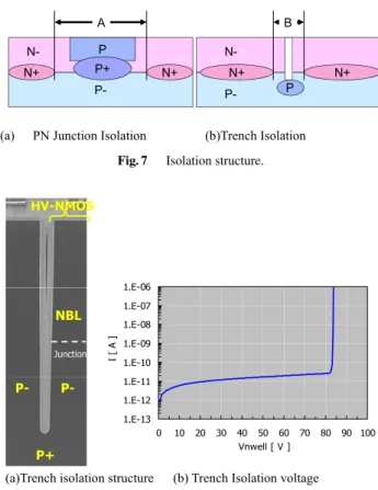
3.1.3 Isolation Area Shrinking
Every device is formed in the “pocket”, in which it is iso- lated by a PN junction or by trench isolation. Therefore, the isolation area is as important as the devise itself. Figure 7 in- dicates the isolation structure. Figure 7(a) shows a PN junc- tion isolation and Fig. 7(b) shows a trench isolation. If we need 80 V isolation in our PN junction isolation, length A in
Fig. 7 Isolation structure.
Fig. 8 Isolation structure.
Fig. 7(a) should be larger than 30µm (0.5µm BiC-DMOS device). However, in the case of trench isolation, Length B in Fig. 7(b) needs only larger than 6µm (0.15µm BiC- DMOS). Therefore, trench isolation can shrink the isolation area by 1/5.
Figure 8 shows the trench isolation structure (Fig. 8(a)) and isolation breakdown voltage (Fig. 8(b)). Although the trench isolation structure has a high aspect ratio, the etched trench shape and burying trench show very good results. As trench isolation has an air pocket, it helps improve the de- vice characteristics [7]. And breakdown voltage is higher than 80 V.
3.2 SOI Device Technology
3.2.1 Features of SOI Device Technology
SOI products have been in production. High performance technology has been further developed. Figure 9 shows an SOI structure with trench isolation filled with silicon oxide.
SOI (Silicon on Insulator) wafer has a shape in which silicon oxide (SiO2) is filled between silicon layers like a sandwich.
If we make a trench isolation filled with silicon oxide in the SOI layer, the silicon area surrounded by silicon oxide is perfectly isolated, as shown in Fig. 9. Each device is formed in this isolated silicon area. Therefore, SOI technology has the following advantages in comparison with silicon bulk technology.
(1) Parasitic action is small.
Fig. 9 SOI structure filled with silicon oxide.
Fig. 10 HVNMOS structure.
Fig. 11 Equipotential line in 160 V Diode.
(2) Negative/multi-voltage input applications are possible.
(3) High Voltage devices are possible.
(4) There is no PN junction in the isolation area.→Suitable for high temperature applications.
Disadvantages of SOI technology are as follows:
(1) SOI material is expensive.
(2) Thermal resistance is higher owing to silicon oxide.
SOI device technology has both advantages and disadvan- tages. Therefore, we should use it properly.
3.2.2 SOI Device Technology
Figure 10 shows a HVNMOS structure in SOI technology, in which devices can be realized from 40 V to 200 V [8].
Figure 11 shows the electric equipotential line for a 160 V diode. The equipotential line is laid in the bottom oxide (BOX) layer. This bottom oxide layer can sustain the elec- tric field and contributes to vertical breakdown voltage as
Fig. 12 Cross sectional structure of lateral IGBT.
Fig. 13 Collector current vs. Collector Voltage (Ic-Vc) Curve.
voltage increases. As the device area is completely isolated, a lateral IGBT (Insulated Gate Bipolar Transistor) is real- ized in SOI technology. Figure 12 shows the IGBT struc- ture, which is formed without additional mask steps. Fig- ure 13 shows the collector current vs. collector voltage (Ic - Vc) curves. A 170 V IGBT current at Vc=5 V is more than 3 times higher than that for 170 V DMOS. And even a 200 V IGBT current at Vc=5 V is higher than that for 170 V DMOS.
Further novel and useful technologies have contributed to Mixed Signal LSI. Without going into details, minor- ity carrier injection prevention [9], thermal-SOA evaluation/ improvement [10], FPMOS current drivability enhancement [11], and pulse stress evaluation to SOI devices [12] have contributed to size reduction and the increased reliability.
4. Novel BEOL Transistor
The BEOL (Back End of Line) transistor is the TFT tran- sistor formed in the metal layer. This transistor uses a wide- bandgap semiconductor InGaZnO (IGZO) as its N-type TFT channel material, Cu metallization as its gate material, and silicon nitride (SiN) as its TFT gate insulator, respectively [13]. Figure 14 shows a cross section of a BEOL tran- sistor. As BEOL transistors can be formed with the addi- tion of a single mask and is formed on the silicon three- dimensionally, BEOL transistors are cost competitive. And
Fig. 14 SEM Photo for BEOL transistor.
Fig. 15 Drain Current vs. Drain Voltage (Id-Vd) curve in BEOL transistors.
Fig. 16 Gate leakage current with drain voltage change in BEOL transistors.
as BEOL transistors are formed on the silicon substrate, which is completely isolated in the silicon, noise and inter- ference tolerance become better.
Figure 15 indicates the drain current vs. drain voltage (Id-Vd) curve. The Id-Vd curve has the good TFT char- acteristics, which can be controlled by gate voltage. Fig- ure 16 shows the Ig (Gate leakage current)-Vd curves with offset length change between gate and drain from 0.1µm to 0.3µm. Figure 17 shows the Gate/Drain offset length de- pendence of breakdown voltage, made using Fig. 16 data.
The breakdown voltage for BEOL transistors rapidly in- creases from 40 V to 80 V if the offset length is extended from 0.1µm to 0.3µm, as shown in Fig. 17. This means BEOL transistors will be very useful for high voltage de- vices.
P type BEOL transistors have been already developed
Fig. 17 Gate-Drain offset length dependence of breakdown voltage for BEOL transistors.
Fig. 18 Past and future technology in Mixed Signal LSI.
Table 2 BEOL Transistor Circuit Usage.
using SnO material as a P-type TFT channel material, as well [14]. BEOL transistors have become to be used in CMOS circuits by P type BEOL transistor development.
BEOL transistors are used for Input/Output circuits, ESD protection circuits, etc. [15].
5. Past and Future Technology in Mixed Signal LSI We have already spent some time discussing past and fu- ture technology in Mixed Signal LSI. Here, we wrap up the earlier discussion. Figure 18 shows past and future technol- ogy for Mixed Signal LSI. Mixed Signal LSI was divided into analog IC, digital IC and power MOS FET transistors.
At present, Mixed Signal LSI uses BiC-DMOS technology, which integrates analog circuits, digital circuits, power tran- sistors, and MCU/ROM/RAM, etc. BEOL transistors will be used in input/output circuits and ESD protection circuits, etc. in the near future. The input/output circuit is formed in the metallization layer, which is over the silicon. More and more circuits using high voltage devices will be formed in the BEOL transistor, as shown in Table 2. Finally, mixed signal LSI with embedded power transistors will become CMOS LSI and BEOL transistors. That is every Mixed Sig- nal LSI will be able to use MCU or SOC by including BEOL transistor circuits.
6. Conclusion
We discussed Mixed Signal LSI technology with embed- ded power transistors. Mixed Signal LSI has progressed rapidly from discrete analog/digital/power IC to integrated BiC-DMOS LSI with MCU/ROM/RAM, etc. Fine fabri- cation technology and SOI technology has contributed to the development of Mixed Signal LSI. BEOL transistors us- ing InGaZnO or SnO as a channel material have also been developed. BEOL transistors were used for I/O circuits or ESD protection circuits at first and will be used for more and more circuits. Mixed Signal LSI will advance further with the support of fine production technology, SOI technology, and BEOL transistor technology, etc.
Acknowledgments
The authors would like to thank the staffof the Mixed Signal Technology Dept. and Advanced LSI Devices Research of Renesas Electronics Corp. for their extensive support and valuable contributions.
References
[1] Y. Sugawara, “Chapter8 power IC,” in Handbook of Power device/ Power IC, pp.187–247, Korona-sha, Tokyo, 1996. (in Japanese) [2] C. Contiero, P. Galbiati, M. Palmieri, G. Ricotti, and R. Stellaand,
“Smart power approaches VLSI complexity,” Proc. 10th ISPSD, pp.11–16, Kyoto, Japan, June 1998.
[3] C. SZ ´ASZ: “Development strategy of next generation single chip smart inverters for motor control applications,” Proc. Mediterranean Conf. on Control and Automation, no.T28-006, pp.1–5, Athens, July 2007.
[4] T. Segawa, “Digital control merit for power electronics,” Transistor Technology, vol.46, no.9, pp.63–153, 2009. (in Japanese)
[5] T. Terashima, F. Yamamoto, and K. Hatasako, “Multi-voltage device integration technique for 0.5µm BiCMOS & DMOS process,” Proc.
12th ISPSD, pp.331–334, Toulouse, France, May 2000.
[6] S. Yanagi, K. Onishi, H. Kimura, T. Kuroi, T. Nitta, and K. Hatasako,
“0.15µm BiC-DMOS technology with novel stepped-STI N-channel LDMOS,” Proc. 21st ISPSD, pp.80–83, Barcelona, Spain, June 2009.
[7] K. Onishi, Y. Otsu, T. Miyajima, K. Morii, K. Furuya, K. Hatasako, et al., “Evolution of trench isolation with air gap in high voltage IC process,” Proc. Joint Tech. Meeting on Electron Devices and Semi- conductor power converter, Shizuoka, Japan, EDD-12-47/SPC-12- 120, pp.23–28, Oct. 2012. (in Japanese)
[8] T. Nitta, S. Yanagi, T. Miyajima, K. Furuya, Y. Otsu, H. Onoda, and K. Hatasako, “Wide voltage power device implementation in 0.25 mm SOI BiC-DMOS,” Proc. 18th. ISPSD, pp.341–344, Naples, Italy, June 2006.
[9] T. Nitta, Y. Yoshihisa, T. Kuroi, K. Hatasako, and S. Maegawa, “En- hanced active protection technique for substrate minority carrier in- jection in smart power IC,” Proc. 24th ISPSD, pp.205–208, Bruges, Belgium, June 2012.
[10] T. Nitta, A. Omichi, S. Yanagi, Y. Yoshihisa, T. Kuroi, K. Hatasako, and S. Maegawa, “Practical approaches to improve thermal SOA for smart power IC,” Proc. 23rd ISPSD, pp.344–347, San Diego, USA, May 2011.
[11] S. Tokumitsu, T. Nitta, T. Shiromoto, T. Kuroi, K. Hatasako, and S. Margawa, “Enhancement of current drivability in field PMOS by
optimized field plate,” Proc. 22nd ISPSD, IC-P4, pp.253–256, Hiro- shima, Japan, June 2010.
[12] T. Nitta, S. Yanagi, T. Igarashi, K. Hatasako, S. Maegawa, K.
Furuya, and T. Katayama, “Necessity of pulse hot carrier evalua- tion in suppressing self-heating effect for SOI smart power,” Proc.
21st ISPSD, pp.84–87, Barcelona, Spain, June 2009.
[13] K. Kaneko, H. Sunamura, M. Narihiro, S. Saito, N. Furutake, M.
Hane, and Y. Hayashi, “Operation of functional circuit elements us- ing BEOL-transistor with InGaZnO channel for on-chip high/low voltage bridging I/Os and high current switches,” Proc. 2012 Sym.
on VLSI Technology, pp.123–124, Honolulu, USA, June 2012.
[14] H. Sunamura, K. Kaneko, N. Furutake, S. Saito, M. Narihiro, N.
Narihiro, M. Hane, and Y. Hayashi, “High On/Off-ratio P-type oxide-based transistors integrated onto Cu-interconnects for on- chip high/low voltage-bridge BEOL-CMOS I/Os,” Proc. IEDM, San Francisco, USA, Dec. 2012.
[15] K. Hatasako, F. Yamamoto, A. Uenishi, T. Kuroi, S. Maegawa, and Y. Fujiwara, “ESD robustness improvement for integrated DMOS transistors,” Trans. IEE Japan, vol.6, no.4, pp.361–366, July 2011.
Kenichi Hatasako was born in Oita, Japan, in 1958. He graduated with a degree in electri- cal engineering from Osaka University in 1981.
He entered Mitsubishi Electric Corp. in 1981 and transferred to Renesas Technology Corp. in 2003 and then to Renesas Electronics in 2008.
He has been developed BiCMOS, BiC-DMOS devices and LSIs. His interests are in analog devices, power devices, ESD, and their applica- tions. He has a Ph.D. in Engineering. He is a member of the Institute of Electrical Engineers of Japan, and the institute of Electronics, Information and Communication Engineers.
Tetsuya Nitta received an M.S. degree in physics from Osaka University, Japan, in 1996. He joined Mitsubishi Electric Corpora- tion’s ULSI Laboratory in Itami, Japan, in 1996, and now works for Renesas Electronics Corp.
He has worked on the development of several power devices, including SJ MOS and Trench IGBT. He is currently engaged in the develop- ment of BiC-DMOS technologies and devices.
Masami Hane received an M.S. in electrical engineering and a Ph.D. from Keio University, Yokohama, Japan, in 1987 and 2003, respec- tively. In 1987, he joined the Microelectron- ics Research Laboratories at NEC Corporation, Kawasaki, Japan. In 1993–1994, he was a Vis- iting Scholar at Stanford University, Stanford, CA. In 2008–2010, he was one of the project- leaders of IBM Albany Nanotech, Albany, NY, as an assignee of Renesas Electronics Corpora- tion. Currently, he is a department head of the Smart Macro R&D Dep. in the New Core-technology Division of Renesas Electronics Corp. He is a member of the IEEE Electron Devices Society, and the Japan Society of Applied Physics.
1996 respectively. He joined the LSI Labora- tory of Mitsubishi Electric Corporation, Itami, Japan, in 1982, and now works for Renesas Electronics Corp. He was previously engaged in the R&D of imaging devices, poly-Si TFT, SRAMs, SOI devices and analysis technology.
Presently, he is responsible for the R&D of ad- vanced mixed-signal devices. He received 2000 R&D 100 Award for the SOI communication LSI. He is a member of the Japan Society of Applied Physics.