Optical Studies on the Trapped Excitons in the Layered Crystals of Cadmium Halides
journal or
publication title
福井大学工学部研究報告
volume 31
number 1
page range 53‑80
year 1983‑03
URL http://hdl.handle.net/10098/4153
FUKUI UNIVERSITY vo L. 31 No. 1 1983
Optical Studies on the Trapped Excitons in the Layered Crystals of Cadmium Halides
, * * **
Hlroaki MA'ISUMOro, Hideyuki NAKAGAWA, Shin-ichi KONOO ( Received March 1, 1983 )
The main subject in this paper is the excitons produced by the optical method in the cadmium halides. It consists of four parts, the 1st part is the studies on Urbach rule applicable to the optical absorption edges, the 2nd is on
refl~ction spectra which corresponds to the absorption due to the exciton creation, the 3rd is on the emission spectra of the relaxed excitons, and the 4th is on the emission spectra of strongly excited crystals.
1. Crystal Structures
Cadmium halide crystals of the interest in this paper are con- fined to cadmium chloride, cadmium bromide and cadmium iodide, and cadmium fluoride is excluded.
c
The formers are layer type crystals and the latter is not.
c-axis
I
• Cadmium 0<=.:0::'-.-,.0 Ion
D~d o Chlorine
Ion
CdCI2
~=:Q~'O D-_-'()::::<:J
•
.. -=tIII·~~~~;:"-
0<::-- : : >0 C. . ...= ~: -:,:-- . O:-'--o-:~" a
0-" :::Q-_-"'O
•
• Cadmium 0:_--0;:.-.:0 IonD5d o Iodine
Ion
Cdh
Fig .1. Crystal Struc- tures of CdCl
2 and Cd1 2, The left is the typical structure(6H) of CdCl
2 and CdBr2,
The right is the typical structure (2H) of Cd 12"
*Dept. of Electronics, **Dept. of Applied Physics
Crystal structures1bf cadmium halides are shown in Fig.l.
Left half of Fig.l is CdC1
2 crystal which belongs to standard CdC12 type structure whose space symmetry belongs to D~d.
Their halogen ions compose cubic closed packing.
Right half of Fig.l is CdI 2 type structure which belongs to Djd space symmetry group.
Their halogen ions compose hexagonal closed packing.
In the figures, black circles are cadmium ions and white circles are halogen ions.
An unit cell, shown with solid lines, contains one cadmium ion and two halogen ions.
As a whole, both structures have layer array of ions perpendicu- lar to the c-axes and an unit layer is composed of two atomic planes of halogen ions and one atomic plane of cadmium ions lying between two halogen planes.
It is well known that the intra-layer coupling of ions is ionic type, and the inter-layer coupling is mainly Van der Waals type.2)
2. Coupling strength between Excitons and Crystal Lattice As the first, we begin with Urbach rule. 3 ),4), 6)
As for Urbach rule, in the optical experiment, at the low energy tail of the exciton absorption spectra of many crystals, values of the absorption coefficient obey to the formula:
( 1)
where K is absorption coefficient, Ko is a constant, a ,steepness parameter, the values of which depend upon the temperature, Eo' a constant corresponding to the photon energy of the lowest exciton peak, E , photon energy, k B , Boltzmann's constant and T is the temperature. This is known as Urbach rule.
Although Urbach rule might be found experimentally, theoretical interpretation has been examined by many physicists. S),6),7),9),9) If Urbach rule stands well, values of absorption coefficient for the absorption edge measured at various temperatures can be shown as straight lines in Fig.2. Then, we can get the values of Eo, Ko as the converging point of these lines and the values of a from the gradient of lines for respective temperatures.
As for the steepness parameter a, Mahr-Keil's formula are known as a function of temperature and energy of phonons which interacts with excitons:
~
t-Z u W
tL
u..u
~ o z a. t=
o
ct:tf) (()
<t
PHOTON ENERGY: E
a
Fig.2. Schematic diagram of Urbach's rule.
Ordinate shows the values of logarithmic absorp- tion coefficient.
Absorption coefficients for the fundamental edge measured at a temperature form a straight line in the logarithmic scale of ordinate. Straight lines of various temperatures converge to a point (Eo.Ko)
in the diagram. where EO is a effective photon energy of an.exciton peak and Ko corresponds to the absorption coefficient of the exciton peak.
(2)
where ao is a constant, ~w: phonon energy.
The value of a shows the strength of the interaction between the lattice and the exciton.
As a = s/g where S is a constant called steepness index and discussed by Schreiber 9) in detail, g is a scale of the interaction strength between lattice and exciton and called exciton-phonon cou- pling constant. Usually, the value of a is used to see the degree of the localization of an exciton in the lattice, that is, if the value of a is less than unity, exciton is self trapped, if the value of a is larger than unity, exciton is free.
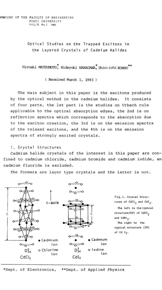
Urbach tails obtained in our experiments are shown in Fig.3, fig.4 and Fig.S for CdCI2, CdBr2 and CdI2 respectively within the temperature range from 80 K to 500 K. A break of Urbach rule is seen in CdCl 2 and CdBr2 at low temperature. It owes to the exist- ence of absorption bands of impurity halogen ions in the crystal at lower energy side of the intrinsic exciton bands.
In CdI 2 , Urbach rule stands well, since other halogen ions con- tained in CdI2 do not usually affect the absorption edge.
In general, at high temperature, Urbach rule stands well for wide range of values of absorption coefficient in absorption spec- tra of CdC12' CdBr2 and CdI2'
Values of steepness parameter a also obey Mahr-keil's formula
....
w z
ul
LL LL UI o
U Z o
;:::
0. a:
o If)
m
"l
.... 10 z w
;:;: u
LL UI o
U
z o ;:::
0.1 a:
o III m
"l
"'ig. 3. Logarithmic absorption coefficient of the fundamental absorption edge of CdC1
2 .
Circles show the measured logarithmic absorption coe f f ic ien ts .
Straight lines are fitted to the Urbach t s rule.
At low temperature, dominant deviation from the Urbach t s rule appears becouse of the existence of halogen impurity absorption bands.
z o
~ 10 c:r:
o <11 CD
"l
3.6 )
rig. 4. Logarithmic absorption coefficient of the Fig. 5. Logarithmic absorption coefficient of the fundamental absorption edge of CdBr 2' fundamental absorption edge of Cd 1
2,
Urbach t s rule stands well in low temperature region for Cd 1
2,
0.7 0.6 0.5
0-
0.4
0.1
100 200 300 400 500
TEMPERATURE (K)
Fig. 6. Temperco.ture dependences of the steepness parameters of CdCl 2, CdBr 2 and Cd 1
2.
Triangles, squares and circles show values obtained from the gradients of the straight lines in Fig. 3, 4 and 5 for CdCl
2, CdBr 2 and Cd 12 respectively.
Broken line, chain line and solid line are fitted ones to the Mahr-Keil' s formula for CdCl
2, CdBr
2 and Cd 12 respectively.
Table I. Values of Urbach Parameters
I
EO ( eV ) KO (cm-l )°0 11w (meV) CdC12 6.31±0.03 (10±1) x 108 O. 70± O. 01 59 ± 5 CdBr2 4.95±0.03 (3 ±1)XI08
o .
79± 0.01 35 ± 4 Cd 12 3.63±0.03 (3 ±1)XI06O.709±O.OOl 12.1±O.6
well as shown in Fig. 6.
Values of 00 and ~w are obtained as shown in Table I.
Situation of
°
less than unity is attained for CdC1 2 , CdBr2 and Cdl2·This means that excitons would have strong interaction with lattice and they would be apt to be trapped at lattice sites in cadmium halide crystals.
Values of average phonon energy obtained from Urbach rule do not agree well with that obtained from infrared absorption11)or Raman scattering12).13~xperiments in some cases.
In Cdl2' a phonon energy obtained from the Raman scattering experiment agrees very well with that of 12.0 meV obtained in our Urbach experiment.
As for the values of Eo' they would correspond to the values of photon energies of excitons obtained in the reflection spectra, which will be talk about just later.
3. Optical Reflection Spectra
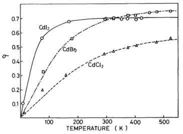
In Fig. 7 are shown the reflection spectra of CdC1 2 measured at LNT. R~ is the reflection spectra measured by the light polarized perpendicular to the c-axis of the crystal. 14)
R# is the reflection spectra measured by the light polarized parallel to the c-axis of the crystal.
40
~30
>-
~ ;;:
i= u20 w --l lJ..
UJ a::
10
----baseline for R ... (cleaved) - - - - 0~--~----~7---8~----~--~
PHOTON ENERGY (eV)
Fig. 7. Reflection spectra of Fig. 7. Reflection spectra of CdCl
2. Spectra were measured for nearly normal incidence.
R~ (cleaved) is the spectra of reflec- tion from the as cleaved surface for R ...
R ... (polished) and R,,(polished) are spectra of reflection from the polished surface for R.I. and R I( respectively
Peaks X, (Xl' Xi), (X 2 , X
2)
are exciton peaks of the lower energy region and S, A, B, B', C are that of interband energy region.The most remarkable difference between spectra R.L and R 1/ is the behaviour of the peaks Xl and A, both of which are very dominant in
R~ and disappear in Rn •
The next difference between R. and Rp is that of X, B' and of X , B, the former two peaks appeared stronger than the latter two in Rn but they do not so in R~.
These anisotropic nature of the exciton peaks will be able to be explained in terms of the models, which will be refered later.
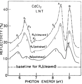
In Fig. 8are shown reflection spectra of CdBr2 measured at LNT, the features seem to be same as that of CdCl2.
In Fig. 9 are shown reflection spectra of CdI2 measured at LHeT, as a whole, they have the same features as that of CdCl2, however some new peaks appear in the spectra, which have not been explained as yet.
50
40
~ 30
>-
f--
>
tJ
20w
~ I.L W 0::
10
CdBr2 LNT
----baseline for R~(cleaved)---
0L--~--~6~--~7--~~-~
PHOTON ENERGY (eV)
Fig. B. Reflection spectra of CdBr 2.
... 50
~
>-
~40 >
i= u w Li30
0:::
w
2010~---+----~~----~----~
PHOTON ENERGY
Fig. 9. Reflection spectra of Cd 1 2.
~he photon energies of the reflection peaks are listed in Tablerr for R~ spectra of CdCl2' CdBr2 and CdI2. The peak energies which agree with the Eo of Urbach rule are underlined. The energies in parentheses correspond to the peaks which disappear in RU spectra.
Table n. Peaks in
Peak CdC1
2
X 5.94 eV
Xl (~)
X~
X2 6.5
X' 2 6.89
S 8.16
A 8.49
B 9.02
B' 8.09
C
the Reflection Spectra
CdBr2 Cd I2
!:.2..Lev 3.8 eV (5.14 ) ( 4.04) (5.37)
5.69 4.58
5.92 6.92
7.17 5.69
7.45 6.22
7.56 6.15
8.91 6.51
(R ... )
The values correspond to the values of EO of Urbach are underlined.
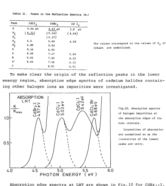
To make clear the origin of the reflection peaks in the lower energy region, absorption edge spectra of cadmium halides contain- ing other halogen ions as impurities were investigated.
1.0
0.5
4.0 K
ABSORPTION
LNT
- >Kmax
4.5 5.0 5.5
PHOTON ENERGY (eV)
\
\
\
,
6.0
Fig.10. Absorption spectra of halogen impurities at the absorption edges of the host crystals.
Intensities of absorption are normalized so as the intensities of the lowest peaks are uni ty.
Absorption edge spectra at LNT are shown in Fig.IO for CdBr2:I, CdCI 2 :I and CdCI 2 :Br.
In the case of the halogen impurity of which electron-affinity is less than that of the host halogen, new absorption peaks were observed in the lower energy side of the intrinsic exciton absorp- tion edge. Difference between photon energies of impurity peak and exciton peak of host crystal shows nearly same values as that of the difference of electron affinities between impurity and host halogens as shown in Table TIr. These facts suggest that the exciton peaks in the lower energy region would be associated to the transi- tion from the valence band orbit composed of halogen valence p- orbitals to an orbit of Cd metals in the bottom of the conduction
band.
Table III. Absorption Peaks of Impurity Halogens in Cadmium Halides
Host Crystal Impurity Number of E !1 E !1 Ea Halogen Peaks (eV) (eV) (eV)
CdC12 Br
2 1 5.68 0.26 0.2
CdC12 12 2 ~.03,5.42 0.91 0.6
CdBr2 12 1 4.57 0.36 0.39
E: peak energy of.impurity halogen, !1E: energy difference between absorption peaks of impurity halogen and exciton of host crystal. !1Ea: difference of the values of electron affinities between impurity halogen and host halogen.
As an exciton model in lower energy region, which satisfies the anisotropic nature of X, Xl and X2 peaks, i t is possible to intro- duce a system of an electron transfered from a valence band orbit made with p-orbitals of halogen ions into the lowest conduction band orbit made with 5s-orbitals of cadmium ions and a hole left in the valence band orbit.14)
For CdI2' this system is illustrated in the lower part of Fig.ll, where X (r
4)
is a orbit built with a dominant pz-like and a small amount of Px' Py like components, Xl(r s' r 6)
is the orbits pure Px' Py like: degenerated from time reversal symmetry, X2 (r4)
isa orbit composed of a dominant Px' Py like and a small amount of Pz components
Cd-5s ___ j = 1/2 __
atomic spin-orbit orbital
spin-orbit
+
crystal field
_~ ___ Cd-5s C.B.
crystal atomic fietd orbital
D3 d
Fig .11. Energy scheme of the excitons in Cd I
2.
Marks:£ and
2
show the tran- sitions observed R.L and RII spectra respectively.Notations C.B. and V.B. are abbreviations of conduction band and valence band respec- tively.
Experiment showed Xl peak disappeared perfectly in Rn spectra, so that, Xl orbit must contain only Px' P y orbitals and this can only be achieved at the high symmetry point in the Brillouin zone,
perhaps at r point.
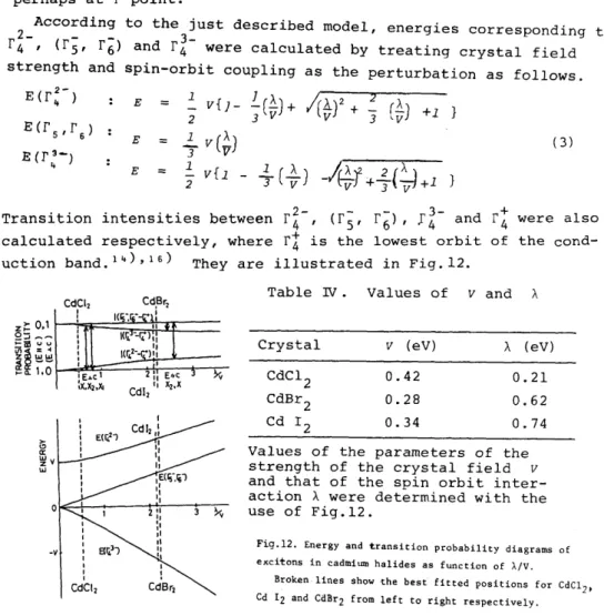
According to the just described model, energies corresponding to
2_ - - 3
f4 '
(r
S 'r
6 ) andr
4 - were calculated by treating crystal field strength and spin-orbit coupling as the perturbation as follows.2-
~(~)
+/(}.y
E(f4 )
E 1 2
_ v{j- (~)
3'v V + +J. }
E(f s ,f6) 2 3 I.V
E
~
v (;) (3)E (r :-)
E 2 !:.. V{l - 3 1 ( -V) A
-if
V At +2.(~)
3 V +1 }Transition intensities between r~-,
(r S' r 6),
J~- andrt
were also calculated respectively, wherert
is the lowest orbit of the cond- uction band.14 ),lS) They are illustrated in Fig.12.Yv
Table IV. Values of v and A
Crystal v (eV) A (eV)
CdC12 0.42 0.21
CdBr2 0.28 0.62
Cd 12 0.34 0.74
Values of the parameters of the strength of the crystal field v and that of the spin orbit inter- action A were determined with the use of Fig.12.
Fig.12. Energy and transition probability diagrams of excitons in cadmium halides as function of A/V.
Broken lines show t:he best fitted positions for CdCI2' Cd 12 and CdBr2 from left to right respectively.
Energy in the ordinate is shown in the unit of v , and unit of abscissa is given in A/V, where crystal field strength parameter v is the strength of the crystal field splitting between
rz-
andr2-
in the absence of spin-orbit interaction and A is the parameter of spin-orbit interaction.
The values of A and V can be determined consistently by applying the experimentally obtained intensity ratioes of absorption bands and photon energies of absorption peaks as shown in the Table N for CdC12,CdBr2 and CdI2 respectively.
Values of A are not so far deviated from that of free halogens.
Though values of A and v are in same order, the value of v is larger than that of A in CdClZ but in contrary the value of A is
lager than that of v in both CdBr2 and CdI 2 .
The energies of
(r;,
r~)
do not depend on the values ofv.
This plays important role in the interpretation of CdCl2-CdBr2 mixed crystal experiments. IS)
In the mixed crystal of CdCl 2 and CdBY2' energy positions of peaks X, Xl and X2 shift as the mixing ratio of CdC12 and CdBr2 varies as shown in Fig.l3. IS)
Peaks X and X2 shift their energy positions smoothly as the mix- ing ratio varies, we call this type of peak as an amalgamation type, the other band, peak Xl does not show smooth shift of its energy position. Xl in CdBr
2 goes into the Br--impurity peak in CdCl2 and does not join to the energy position of Xl in CdCl2' we call this type as a persistent type.
CdBr
2b\
\ \ -~ , \J....N
• • •
CD -0
0.8
o • \ 1 \ \ \•
\ \•
\ \•
~ \X~
U _ 01 ·1
•
\•
\\ CdCI
Z-CdBr
Z~
o~
\ \X;
0
\ \ \ • LNT
Fig.l3. Energy shift ofZ
0.6 - \X2
exciton peaks in CdClz: CdBr Z0
\ .X .X
l- \ \ \
mixed crystals.t-
<t: 0.4 -
\ \\ •
Eg: Energy of band edge.0::
X\ \
t-
xi
z 0.2 Eg \ ,,\ .\ .\
w - ..
u \ . \ .
\ \ \Z \
. . ,
I
'-o~\'.~L~ \\ •
8 Cdel
2\
A - O - .
•
5 6 7
PHOTON ENERGY (eV)
This nature of Xl peak is consistent to the model where Xl cor-
respond~ to the transition from
(r s' r 6)
orbits. The energy of (f S ' f6) is not affected by the strength of crystal field v and Xl peak may be persistent type in the mixed crystal of CdC1 2-CdBr 2 ·As for the structures in the deep inter-band region, sharp lines A, B, B', etc. appeared in the energy range of more than 2 eV high- er than the band gap energies as shown in Figs. 7, 8 and 9.
The most noticeable feature of these structures is the aniso- tropic nature of A, which perfectly disappears in R" spectra as Xl does. This fact suggests that the initial state for the transi- tion corresponding to A does not contain Pz component. This may attribute the transition as that at high symmetry point of Brillouin
zone, perhaps at some point between rand Z points in CdCl 2 and CdBr2 and between
r
and A points in CdI2.As has been known in CdI 2,18)
r 2
andr;
orbits have a large dis- persion along k z axis in Brillouin zone. Same situation would be valid for CdCl2 and CdBr2' so a level scheme such as shown in Fig.l4 can be imagined.WN· ,~
(R~<~_ "b4;;::.:j:
. . ';\~
34- . . .
4- 4-
Z
Brillouin Zone
Fig.14. Exciton energy diagram and optical transitions at energies of both low and deep regions.
The right part: energy scheme of low energy exciton transitions at r point in Brillouin zone (sho~ at the lower part in the figure)_
The left part: energy scheme of deep energy exci ton transitions at Z point ( CdCl
2• CdBr 2) or A point ( Cd 1
2) in Brillouin zone_
The orbits 5 and 6 are pure (p
x, Py) like and two 4 orbits contain Pz, PX' Py symmetry. This can explain the anisotropic nature of A, B, B'. A can only be seen in R~ spectra and B' is rather dominant in
Rn
spectra.4. Intrinsic Emission Spectra
When cadmium halide crystals were excited with light in the energy region of excitons, intrinsic emission spectra were observ- ed~19),20),21),22)
In cadmium halides, as a whole, the emission barns can be clas- s i f ied in three ca tegor ie s accord in g to the i r pho ton en ergy reg jon s : UV-emission; ultraviolet region above 3.0 eV,
G -emission; green region near 2.5 eV, Y -emission; yellow region near 2.2 eV.
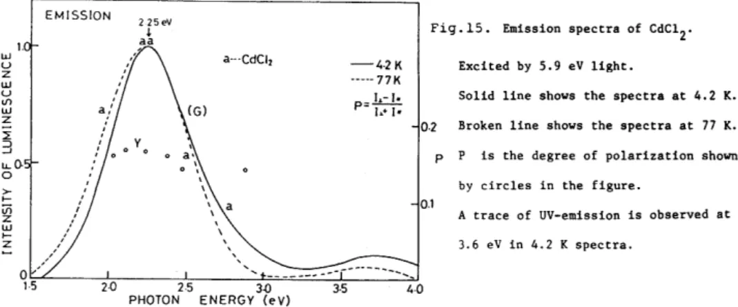
In Fig. 15, are shown the emission spectra of cadmium chlorides excited with 5.9 eV light at LHeT and LNT and their degree of polarization at LNT which are shown by small circles.
u w z w u
If) w z ::E 3
1.
ll..Q.
o
>-
I -
iii z
W I - Z
EMISSION
~/
I I
I 0
225eV aa ~
a---CdCI2
2·5 3.0
PHOTON ENERGY (eV)
Fig. 15. Emission spectra of CdC1 2. -4·2 K Excited by 5.9 eV light.
---77K
I.-I. Solid line shows the spectra at 4.2 K.
P=~
0.2 Broken line shows the spectra at 77 K.
P P is the degree of polarization shown by circles in the figure.
0.1 A trace of UV-emission is observed at
3.6 eV in 4.2 K spectra.
4·0
The degree of polarization is defined here as I.J,.. - III
P = I . + III (4)
where I~ means emission intensity polarized perpendicular to the crystal C-axis, In that polarized parallel to the C-axis.
In cadmium chlorides, UV is very weak and a Y emission (2.25 eV) is dominant in both LHeT and LNT. A trace of G emission (about 2.6 eV) is observable in LHeT.
Values of degree of polarization show that polarization of emis- sion is not so remarkable both in G and Y.
In Fig.l6 are shown the emission spectra of cadmium bromides excited by the light of about 5 eV at LHeT and LNT. A UV emission
(3.30 eV) is dominant at low temperature and though its degree of polarization has a temperature dependence, their values are not high .
wl·0 u z w u
If)
w z ::E
3 g,o.s
>-
I-
iii z
W I - Z
EMISSION
,9. .... ,
"
\I \
I \
I \
I \
b! '.
I \
" 0\ 0
" 0 0 Y077~ \
I \
I \
I \
I \
" bl
/,/ \'"
."
b---CdBr2 330.V
~
..
b .. 4.2~
-4.2K ----17K
0.3
0.2 Fig.16. Emission spectra of CdBr2· P Excited by 5 eV light.
0.1
O~----~~---~~ ____ ~~ ____ ~~~~ __ ~
1.5 2.0 2.5 3·0 4.0
PHOTON ENERGY (eV)
At high temperature (LNT), a Y emission (2.15 eV) becomes domi- nant and UV becomes weak, values of degree of polarization are low and have no temperature dependence.
Emission spectra of cadmium iodides excited by 3.S eV light are shown in Fig. l? A strong G emission (2.50 eV) and a weak Y emis- sion (2.16 eV) were observed at LHeT. An UV emission is very weak at LHeT. This emission becomes strong at very low temperature less than 2 K, which is not shown in the figure.
u w w z
U ."
W Z
s:
::>
...J
1·0
lSO.5
>-
I -
iii z
I -W Z
1.5
EMISSION
2.50eV
,
c
-4.2K ----77 K c----Cdlz
Pd~(3.2~E'V)
!
3.5
+0.3 +0.2
+0.1 f' ig. 17. Emission spectra of Cd 1 2, p
0.0 Excited by 3.8 eV light . -0.1
-0.2
4.0
Intensity ratio of G and Y emissions varies as temperature raises and Y emission becomes dominant at LNT.
Values of degree of polarization have no temperature dependence and are negative for the G emission and positive for the Y emission.
In Fig.lS are shown (a) excitation spectra for Y emission in CdC12, (b) excitation spectra for Y emission in CdBr2 and (c) excitation spectra for Y and G emission in CdI2. These emissions
are all excited only by light in the intrinsic absorption range.
And then, they can be attributed to the intrinsic emissions of the crystals.
There is a list of luminescence of cadmium halides, including values of life time of the emissions measured at 10K in Table V.
The values for the luminescence of the mixed crystals CdC12-CdBr2, CdC12-CdI2, CdBr2-CdI2 are also given in the table. They play
important roles to certify the model of these luminescent centers, or relaxed excitons.
u w w z
u
ll)
w z
L :J -.J LL o
>-
l - ll) Z W I - Z
uJ U Z uJ U If)
W Z
~ :::>
.-J LL 0
>-
l-
ll) Z W I - Z
5·0 u w z w u
If)
w z 2 :::>
--1 LL 0
>-
I - If)
Z uJ I - Z
CdCh LNT
Y
Cd Br2
LNT
PHOTON
5·5Exci.Sp (for 2·" eV emis.) Y
I I I
I I
... / Absorp. Sp.
/ .... ,
I \
I I I
.
I.
I.
I; A BSORP. 5 p.
I I
"
,I
5
»
CD Ulo
:0 CD
»
Z n rn
»
CD Ulo
:0 CD
»
Z n rn
4·0 4·5
PHOTON
5·0 5·55D
1.0 EXCI TATION : LHeT
0.5
ENERGY (eV)
Xz(4.66eVl/ l I
/ - J
for 2.16eV ,
\ emis.
I-
j
BE;
(j) o
::0
"U --i
60 z
\ /:t.~-, ... -- ___ ,
'" ' \
n o
rn OJ
"T1 Xl (4.07evlj'
~ ,
i\../
Indirect ! '
1
Abs. Sp. /
4.0 ENERGY
for2.50eV emis.
G
\
\ n
(Tl
z --i
2~
5.0
0", n 3~
Fig.IS (a). Excitation spectra for Y-emission in
Broken line shows the low energy part of intrinsic absorption.
Fig.IS (b). Excitation spectra for Y-emission in CdBr2·
Chain line shows the position of the absorption edge.
Fig.IS (c). Excitation spectra for Y and G-emis- sions in Cd I
2•
Solid and broken lines show the excitation spectr~
of G and Y-emissions res- pectively. Chain line shows the absorption spec- tra. Dotted line shows the position of the absorp- tion edge. Pb++ shows the excitation for the emission of impurity Pb ++ ions.
Table V. Luminescences of Cadmium Halides Sample Energy (eV) Name Life Time ().Js)
CdC12 3.60 UV 0.2 and 0.7
2.25 Y 380
CdC12:Br 2.65 G 300 and 20
CdC12: I 2.20 Y 300 and 40
CdBr2 3.30 UV 0.9
2.15 Y 200, 20, 4
CdBr2: I 3.35 UV 0.5
2.52 G 8 and 4
Cd 12 3.35 uv 0.3 and 1.1
2.16 Y 20 and 6
Values of the life time w~re measured at 10 K except UV emission.
5. Model of Emission Centers
The fact that every emission has long life time of several ~-sec.
is worth noticing to consider the model of emission centers.
It may be remembered that Urbach rule experiment showed our excitons have a strong interaction with crystal lattice and are apt to be trapped excitons. The trapped excitons relax the lattice near- by and become quasi-stable relaxed excitons. These relaxed excitons may be localized in the crystals. Considering the long life time of our emissions, they may be attributed to the emissions from relaxed excitons.
If we assume the localized relaxed excitonic states as excited states of a complex ion which is composed of a central cadmium ion and surrounding six halogen ions, we can make a schematic energy diaqram as shown in Fig.19.
T,U
np(X), 5s(Cd) 4d(Cd),5s(Cd) (hole, elect ron)
y G
DJd
Eu
A2U Eg
Alg
A2g Eg
Eg UV
c...
A,g UV
ell
Fig.19. Schematic energy diagram of the relaxed excitons.
The right diagram shows the scheme of two compo- nents of UV-emlssion from A2u level.
At the left are shown assumed combinations of orbitals of a hole and an electron which compose a relaxed exciton.
central column shows composite states derived from the combina- tion of such a hole and an electron in the octahedral symmetry.
Right column shows composite states in D3d symmetry. In reality, our complex ion lies in D3d symmetry field in the cadmium halide crystals.
UV emission which can be explicitly observed only in CdBr2 and CdI 2 at low temperature has the highest energy and is attributable to the emission from the one of the highest level A2u to the ground Alg according to the following reason.
The value of life time of UV is the shortest in the intrinsic emission bands, this may connect UV emission to the parity allowed transition from ungerade to gerade. On the other hand, if Eu is the initial state of UV emission, polarization of the emission is perfectly perpendicular to the crystal C-axis, this is not the case.
Further, spin-orbit and electron-hole interactions are taken into consideration, A2u splits into
ri, r 2
andr3
and thenr 2
can connect with ground state radiatively with the light polarized parallel tothe C-axis and
r3
with the light polarized perpendicular to the C-axis.In CdBrz' by investigating the temperature dependence of the polarization ratio IH/I~, we can get the value of energy separation between
r;:
andr;
as 3.3 meV, and can determine ther3
to be the lower.2o)The G emission, which is dominant in CdI 2 at low temperature, can be assigned to a transition from Eg to Al g .
Though this transition is parity forbidden by nature, if a cer- tain odd parity mode lattice vibration or deformation mixes the upper A2 u and Eu to this Eg , the prohibition may be relaxed for the radiative transition between Eg and A1g with both polarizations per- pendicular and parallel to the C-axis.
In CdI2, the temperature dependence of the life time of G emis- sion was obtained as shown in Fig.20(a). This dependence can be explained by taking a thermal interaction between the initial state of G emission Eg and that of Y emission Eg into consideration and making the following rate equation:
dng 8 1
at
N g - (W1 exp (-kBT) +'T!)'
ng t,+ Wz exp (-kB T) •
ny
(5)
•
\
G - emission
• -calcu.
• exper.
\ .~
...
-.-.--
• ( a )
20 40
60
T ( K )I 0
T = WI exp ( -kBTJ
G
( b )
Fig.20.
(a) Temperature depen- dence of life time of G-emission in Cd I
2 . (b) Adiabatic potential
scheme of the levels of Eg(G) and Eg(Y) used in the analysis with eq.(5).
where ng and ny are the population of upper and lower levels of Eg respectively, Ng is the time rate of relaxation from higher levels to the initial state of G emission i.e. upper E g , Tl is the relax- ation time due to the direct transition from upper Eg to the ground AIg states, WI and W2 are thermal activation frequencies from upper Eg to lower Eg and from lower Eg to uppe~ Eg respectively, 6 and 6 are thermal activation energies of upper Eg and lower Eg respective- ly as shown in Fig.20(b). T is the life time of G emission. Making best fit of the calculated values of T (solid line in the figure) to the values of the experimentally obtained relaxation time (solid dots), values of 6, WI' and Tl are obtained as:
6
=
1.84 meV, WI=
7.60 x 10⁵ s-~ Tl 7.55 ~s.As for the Y emission, which is dominant at LNT in every cadmium halide and is located at the lowest energy, may be attributed to the transition from the lowest Eg to the ground A1g states.
In the case of CdI 2 , the Y emission has two kinds of life time:
TS slow component, TF fast component and their temperature depend- ences are shown in Fig.2l.
Taking electron-hole interaction into consideration, Eg splits into lEg and 3Eg • Solving the following rate equations on these states including thermal interaction between them22) :
(6)
d nt
-(Pr t + Sts)·n t + Sst'ns dt
Sst Wst ' «n> + 1) {phonon emission}
Sts Wts·<n> {phonon absorption}
E l}-l.
<n> {exp(kT)
where nand s n t are the population of levels IE g and 3Eg respective- ly, Sst and Sts are the phonon assisted transition probabilities and Frs and F rt are the radiative transition probabilities from lEg and from 3Eg respectively.
Fig.21. Temperature dependence of the life time of Y-emission in Cd 1 2 ,
These were analyzed by best fitting the rate equations (6) to the observed values.
o~ Cdl2
I
\
Ex. at 3.675 eVO~\
... Ts~-
... -
...5 , " .
I ",{-om;,
• ',Tf" .~
\ \
.
\ \V-emis. ' \ .
G-~
\/ \emis .•. ~ \
i'·- \
1
~~:--
\
,
"
0.5
\
I I I I I I I I I I I I
o
50 100 150TEMPERATURE. T(K)
with the use of the values of the parameters as shown bellow, i t is able to fit the measured life times to the calculated ones shown with solid lines in the figure.
Frs 1. 58 x 105 -1
s Frt 4.50 x 10⁴ -1 s Wst 1.10 x 10⁴ -1
Wts 1.67 105 -1
s x s
E 1. 58 meV
'J?he value of the separation between IE g and 3
E g is obtained to be 1.58 meV.
As for the intrinsic emissions, we may conclude that excitons, optically formed in cadmium halide crystals, relax to the localized relaxed excitons, which correspond to the excited states of complex ions [Cd2
+X6]4- in the D3d symmetry crystal field whose schematic
energy diagram is given in Fig.l9.
The A2u state of the complex ion emits the UV emission. Since A2u state may thermally be unstable, CdCl
2 and CdI
2 show the UV emission only at very low temperature.
The Eg(Tl g ) state is also unstable at LHeT in CdCl2 and CdBr2, and the lowest state Eg{E g } is most stable, where the Y emission begins at, Y emission is always dominant at LNT.
Experimental investigation on the mixed crystals of cadmium halides also supply powerfull evidence abundantly.19),20),21)
In addition to these emissions from relaxed excitons, Hayashi et al 13),2~) reported a series of emission bands due to free excitons found in the region of the absorption edge of CdI2.
6. Induced luminescence of strongly excited CdI2
In semiconducting materials including layered structure material, effects of high excitation density (HED) have been studied extensive- ly, where the interaction between excitons and lattice is rather weak and role of free excitons is main concern with respect to the non- linear process involved by strong excitation.25
) ,26) ,27)
It is of some interest to investigate the effects of high exci- tation density (HED) in the system where the interaction between excitons and lattice is rather strong such as in cadmium halide2
s8.-31) As cadmium iodide has optical absorption edge near 3.4 eV, we can use 3.68 eV light from N2-gas laser to excite CdI~ strongly.
Experimental set up is shown in Fig.22.
Monochro- mator Photomultiplier
Fig.22. Experimental set up of the strong excitation of Cd 12 with the use of Nz-gas laser light.
Cadmium iodide has dominant G and weaker Y emissions in the case of the usual light excitation at LHeT as shown in Fig. 23 by dashed line.
w u
z w
U
<Ii
~1.0 ::E :J
IJ..
o
>-- z
EMISSION Cd!,
LHeT
E~citation - N,- laser
(3.68eV) ---- D,-Iamp
(3.68 eV)
Fig.23. Emission spectra of Cd 12 at liquid helium temperature (LHeT).
Broken line: excited by the 3.68 eV light of D2-lamp.
Solid line: excited by the 3.68 eV light of N
2-gas laser.
The intensities of luninescence are normalized to unity at the max- imum.
In the case of high excitation density (HED) with laser light, strong G and Y emissions such as shown in the figure with solid line are observed at LHeT.
There exist some red shifts in the peak energies, and the intensity ratio of Y emission to G emission somewhat increases.
At LNT, though Y emission is dominant in the case of the usual excitation strength (dashed line), G emission is rather stronger than Y emission and emission bands are both sharp, and have red shift in the case of HED (solid line) as shown in Fig.24.
EMISSION w u
w z .,;
u
Vl w 21.
~ :J -'
u.
0
>-
>--0.5 Vl 2 W
>-- 2
Cd I, LNT
E Icitation
- H,-Iaser
(3.6S~V) ---- 0, -lamp ( 3.6S.,V)
P'ig.24. Emission spectra of Cd 12 at LNT.
Dotted line: Gaussian separation of the broken line spectra into Y and G-components.
Dependence of G emission strength upon the intensity of excita- tion light of 3.68 eV was investigated at LNT. Taking the intensity of emission I, intensity of excitation light Io, we obtain the
relation:
where A is constant and values of n are
n = 1 for usual strength excitation light from Xe-lamp, and n 1.6 for HED by N2-laser as shown in Fig.25.
This fact suggests the nonlinear process is concerned in the case of laser light excitation.
w u
z w u
V) w z
i ::::l ...J
lL o
>-
l - V) Z W I - Z
~Cd12
logl LNT 2.37eV
I
LUMI:G i/
4
Ex. at 3.66eV .I'
•• n= 1.6
3f-I---I=A·~ _ _
I
I
/ ',:
/
./2
..
~.'~/ / . n=1
N2-1aser ~ . /
I
J /
If-
/... /~. Xe-Iamp f - - - I ..-
Of-
~/
\ogl.-
o I 2
INTENSITY OF EXCITATION
Fig.25. Excitation intensity depend- ence of the G-emission of Cd 12 at LNT.
N2-laser excitation shoW's super- linear response (n=l. 6) .
Xe-lamp excitation shoW's linear response (n=l).
Further we examined the dependence of G emission intensity upon excitation length on the crystal at LNT.
Shaklee et a132 ) have derived a formula on the relation between emission intensity and excitation length:
I = Is{exp(gLJ - l}/g (7)
where I is the emission intensity, Is intensity of spontaneous emis- sion, L excitation length, g optical gain per unit excitation length.
This formula does not contain saturation effect of induced emis- sion, in reality saturation occurs as shown in Fig.26.
In the unsaturated region, gradient of In(dI/dL) gives optical gain g and we get these values of g for various excitation strengths.
4 -1
High values of g such as 10 cm show that a certain induced
IL o
Stnnul., .. d Emission EAcHI'd Rpgion
.. _-.,XI
--d ... -.
Fig.26. Excitation length dependence of the intensity of the 2.43 eV emis- sion at LNT.
Pumping powers for the curves a, b, c and d are proportional to 1, 1/5, 1/25 and 1/125 respectively •
emission occurs in the case of HED. This is a non-linear emission process.
There is a gain spectrum of the emission for a constant excita- tion strength at LNT in Fig.27. The gain spectrum shows that G emission is most effectively stimulated and V and Y emissions are also stimulated.
GAIN Sp. 't X103
~l
.0
Optical Gain w Cd 12 8u f'
z L NT Excitation
w ,0 0,
U
V) -Nz-Iast'r
-'.I 0
='0 2: ---- Dz -Lamp 6
"
~ Fig.27. Emission and optical gain spectra:J ( 3.S8eV) ('l
of
::> Cd 12 at LNT.
... , 0
o. "
.... \. ~ Chain line is the optical gain spectra.
0 ::>
\ z
:05 \
'.
:.n z
, 3
u.J 2"':
f-z
0 2.0 2.5 0
PHOTON ENERGY
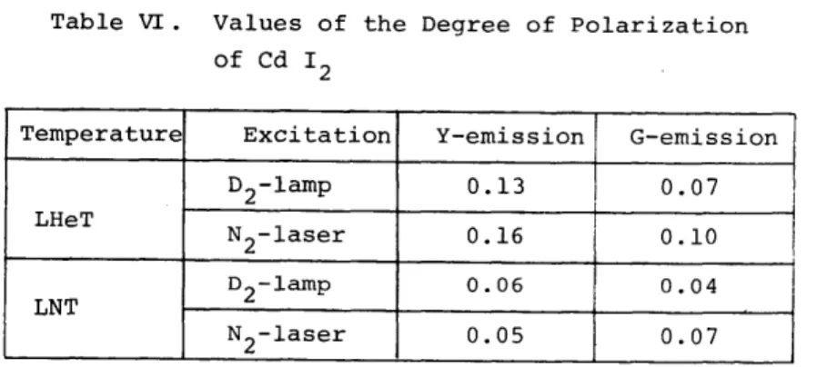
Degree of polarization were measured for the emissions excited with usual and strong lights respectively.
Values of degree of polarization are not different so much each other as shown in Table ~ .
Table VI. Values of the Degree of Polarization of Cd 12
Temperature Excitation Y-emission G-emission
D2-lamp 0.13 0.07
LHeT
N2-laser 0.16 0.10
D2-1amp 0.06 0.04
LNT
N2-1aser 0.05 0.07
1
I
This suggests that emitting centers concerning to both excitation methods are same ones, that is, isolated relaxed excitons.
As for the emission life time in the' case of HED, oscilloscope traces of G emission decay are shown in Fig. 28.
UJ
'i2
UJ u
'"
~oLl~~t=~~~~~~
8 )Is
~ ~~--r-r-.-,--r-r~
.D :;;
~4 lJJ u Z lJJ U 1,/1 lJJ Z
2
- L
"
a
...
i O
~ 0
\>.6 o
2
0
I
~., -,
1 l
Cdlz
~~::isl-L H
Nz-Iaser tx.
l\.
Il'b 1
i... ~ t..a... I
~ 12 16 ).Is
,
Cdlz
LHtT
IJ-
G·~m;s. I - Nz-lastr ex.
c
f\ f -1--
01 0.2
-
OJ 0.4 ).IsTIME
Fig. 28 • Oscilloscope traces of the 2.37 eV emission under strong excitation.
In the figure, a is a whole trace, b : ordinate of a is ten times elongated and this part shows slow component of emission decay, c abscessa of a is ten times expanded and this part corresponds to the fast component of emission decay. Left two are
measured at LNT, right two are measured at LHeT. The slow part of emission decay shows the dependence of excitation intensity.
As the intensity of excitation decreases, decay becomes slower, and in the case of weakened laser excitation, decay time becomes same as that of Y emission excited by the usual light ~ 5.8 ~s.
We can get the time resolved emission spectra for this slow com- ponent by measuring emission intensity at constant delay time for the photon energies in this region~9) These spectra do not show any differences from the emission spectra for the usual light exci- tation. Thus, this slow component corresponds to the spontaneous emission process which competes with the induced emission processes in HED.
The fast components of G emissions for various excitation strength can be fitted to the solutions of a rate equation which contains non linear term, induced emission process, at LNT:
dne
crt
- (A + w) ne ( 8)where - C dne w
crt
These are shown in Fig. 29, here, curve d is a decay curve for spontaneous slow emission of the life time 5.S ~s.
c
DECAY of G-emis.
n.(I=O):n, A=1.71 "10' s"
calcu expe,. c·",
• ···0.90
b - ··0·5'5
• ···0·30
• ···0·0545
~
2'~:"~:::;.~.-..
_ _ _~ 1 Cdi]
~ LNT
°0 1 2
TI ME (jJs)
Fig. 29. Luminescence decay curves for various excitation strengths.
Lines a, b, c and d are the best fit- ted ones with the measured values of life times for respective strengths of excitation by using eq, 8 and the values of its parameters given in the figure.
The rate equation used to fit the experimental results is too simplified one.
If emitting centers are relaxed excitons in the case of HED too, thermal interaction between both Eg levels, which are initial states of G and Y emissions respectively, must be taken into con- sideration to compose rate equations, and rate equations applicable
to these emissions must be simultaneous equations as follows:
(9)
~ d t
Nevertheless, at LNT, values of kBT may be almost equal to the values of ~E, and ~E is far smaller than E as shown in the energy diagram of the exciton system Fig. 30 .
---...: .... R
Fig. 30. The adiabatic potential energy diagram of exciton of Cd 12 ,
The hatched band is the free excitons. R means appropriate lattice sistortion.
In such a case, thermal activation rate sYG from Eg(Y) to Eg(G) may be negligiblly small and then the rate equation for the G emis- sion can be written in a simple form:
- ( A + W dnG d t
-c - - where A equals to AC + SCy and w equals to G dt
This type of simple rate equation is applicab~e ~o the observed strongly excited G emission as already shown in eg. 8
This fact may also support that the emitting centers are relaxed excitons.
As a conclusion obtained from these experiments, strongly ex- cited CdI
2 crystal by 3.68 eV light of N2 gas laser emits short
22)
life induced emission at the energy range of G emission and Y, V emissions
Induced emission is most effective at the energy range of G emission.