Synthesis and Applications of Heterostructures of Two-Dimensional Materials
アザ, スクマ, アジ
https://doi.org/10.15017/1931943
出版情報:九州大学, 2017, 博士(工学), 課程博士 バージョン:
権利関係:
Synthesis and Applications of
Heterostructures of Two-Dimensional Materials
A Dissertation Presented to
Interdisciplinary Graduate School of Engineering Science of Kyushu University
Adha Sukma Aji
2018
Abstract
The potential of atomically thin layered materials, such as zero band gap semiconductor graphene, semiconducting transition metal dichalcogenides (TMDCs), semiconducting metal chalcogenides (MCs), and insulating hexagonal boron nitride (h- BN) are promising for future building blocks of electronic devices. The heterostructures of these ultimate thin materials offer new solutions for the problem in Si-based device miniaturization. For example, graphene with its high conductivity could be utilized as the future interconnection or electrical contact for semiconducting 2D materials. WS
2is a prospective choice for a semiconducting channel owing to predicted high electron mobility that is comparable with carrier mobility of Si. However, the poor electrical contact between single-layer WS
2and conventional metal electrodes retards the carrier mobility of WS
2. In this thesis, the improvement of single-layer WS
2carrier mobility (50 cm
2/Vs) with chemical vapor deposition (CVD)-grown multi-layer graphene (MLG) electrodes is demonstrated. The improved contact is explained by the tunable work function of MLG electrodes that can overcome the high Schottky barrier (SB) height usually formed with conventional metal electrodes. The high mechanical robustness of MLG-WS
2heterostructures allowed the demonstration of flexible fast (response time of 2 ms), and sensitive (responsivity of 4500 A/W) photodetector.
Next, due to its unipolarity of n-type WS
2, it is difficult to form a p-n junction or complementary field-effect transistors (FETs) with solely WS
2. The heterostructures of two different materials with different polarities could solve this problem. Therefore, this thesis also presents the novel SnS-WS
2p-n junctions realized by using two-step CVD method. The SnS (a member of MCs) was found to have a p-type polarity with the mobility of 15 cm
2/Vs. Then, the formation of SnS-WS
2p-n junction was confirmed based on its rectifying behavior. The p-n junction also exhibited a tunable rectification ratio and good ideality factor because of clean interface resulting from two-step CVD method.
Moreover, the presence of SnS could enhance the photodetector performance due to high optical absorption of SnS.
This thesis demonstrates the advantages of two-dimensional-based
heterostructures which can be applied to cutting-edge electronic and optoelectronic
applications in the near future
Table of Contents
Abstract ... i
Table of Contents ... ii
Chapter 1 – Introduction ... 1
1.1. 2D materials beyond graphene ... 1
1.1.1. Graphene and its zero band-gap nature ... 1
1.1.2. Transition metal dichalcogenides and metal dichalcgonides... 4
1.1.3. Heterostructure of 2D materials ... 6
1.2. Motivation ... 8
1.3. Outline of thesis ... 10
Reference ... 11
Chapter 2 - Structure, Electrical Properties, and Preparation Methods of WS
2and SnS ... 15
2.1. Structures of WS
2and SnS... 15
2.1.1. Structures of WS
2... 15
2.1.2. Structutres of SnS ... 16
2.1.3. Phonon modes of WS
2and SnS ... 17
2.1.3.1. Phonon modes of WS
2... 18
2.1.3.2. Phonon modes of SnS ... 19
2.2. Electrical properties of WS
2and SnS ... 19
2.2.1. Band structures of WS
2and SnS ... 20
2.2.2. Expected carrier mobilities of WS
2and SnS ... 22
2.3. Material preparation: CVD growth of TMDCs, MCs, and 2D materials-based
heterostructures ... 24
References ... 28
Chapter 3 – 2D Materials-Based Field-Effect Transistors ... 33
3.1. Field-effect transisotr operation ... 33
3.2. WS
2- and SnS-based FET ... 35
3.3. 2D heterostructures-based p-n Junctions ... 38
3.4. Metal contact to 2D materials-based semiconductor ... 40
3.4.1. Problems on interface between metal and 2D semiconductor ... 40
3.4.2. Schottky barrier extraction: thermionic emission... 41
References ... 44
Chapter 4 – High Mobility WS
2Transistors Realized by Multi-Layer Grapehene Electrodes and Application to High Responsivity Flexible Photodetector ... 49
4.1. Introduction ... 49
4.2. Experimental method ... 52
4.2.1. CVD growth of single-layer WS
2and MLG ... 52
4.2.2. Characterizations ... 53
4.2.3. Device fabrication ... 54
4.2.4. Device measurement ... 54
4.3. Results and discussion ... 55
4.3.1. Fabrication and characterization of WS
2-MLG heterostacked devices . 55 4.3.1.1. Fabrication of WS
2-MLG devices ... 55
4.3.1.2. Characterization of WS
2-MLG devices ... 57
4.3.1.3. Transport properties of WS
2-MLG FET ... 58
4.3.2. Investigation of electrical contact of MLG to single-layer WS
2... 60
4.3.3. Flexible optoelectronic WS
2devices with MLG electrodes ... 66
4.3.3.1. Fabrication and transport properties of flexible devices ... 66
4.3.3.1. Optical response ... 68
4.4. Conclusions ... 71
References ... 73
Chapter 5 – Two-step Synthesis and Characterizations of Vertically Stacked SnS-WS
2and SnS-MoS
2p-n Heterojunctions ... 79
5.1. Introduction ... 79
5.2. Experimental setup ... 81
5.2.1. Two-step CVD growth ... 81
5.2.2. Characterizations ... 82
5.2.3. Device fabrication and measurements ... 82
5.3. Results and discussion ... 83
5.4. Conclusions ... 102
Chapter 6 – Conclusion and Future Outlook ... 109
6.1. Conclusion ... 109
6.2. Future outlook ... 110
References ... 113
Acknowledgements ... 115
Chapter 1
Introduction
1.1. 2D materials beyond graphene
1.1.1. Graphene and its zero band-gap nature
Discovery of exceptional properties of isolated single-layer graphene in 2004 has
triggered many researchers to explore other possibilities of new physical phenomena in
2D structure.
1The isolation to atomic thickness introduces so-called 2D quantum
confinement effect. This effect offers many interesting new properties of graphene, for
example, massless charge carrier in graphene which theoretically predicts that the
carriers in graphene can drift at the speed of light.
2,3At the early stage of graphene’s
finding, the graphene flakes were fabricated by using an mechanical exfoliation method,
where a starting graphite was separated by using adhesive tape repeatedly. Eventually,
due to the low van der Walls interaction in each layer of graphene, the single-layer
graphene could be separated and placed onto the insulating substrate (i.e. SiO
2). The isolation of single-layer graphene allows A. Geim and K. Novoselov to examine electrical properties of graphene by fabricating the field-effect transistors (FETs) with graphene as the channel of a transistor. The report on graphene FET later gave these two researchers a Nobel Prize in 2010.
1For electronic device applications, graphene is very desirable, because it exhibits very high carrier mobility of 2×10
5cm
2V
-1s
-1.
4The exceptional conductivity of graphene was exploited as the electrical contact to the 2D semiconducting material in this thesis.
However, one major drawback of graphene is that graphene does not have a band gap which hinders its application to the logic devices. Two approaches have been proposed to open the band gap of graphene; confining graphene sheet to one-
Figure 1-1. Classification of 2D materials based on their band gaps. Adapted from Ref. 8.
dimensional nanoribbons structure or applying a strong perpendicular electric field to double-layer graphene. For nanoribbon case, the width of graphene is needed to be scaled down to below 10 nm to achieve on-off switching at room temperature.
5In the double-layer graphene, the controlled stacking order (called AB stacking) is required to break the graphene’s symmetry, and the vertical electric field is needed to be applied to open band gap.
6However, the complicated material preparation and device design make these approaches unfavorable for large-scale device production.
To solve this issue, many researchers have shifted or widenend their focus from graphene to other 2D materials to find alternatives. More than 600 layered materials are predicted to be able to be thinned to single-layer form, including 2D material with semiconducting properties.
7Figure 1-1 shows a classification of well-known 2D materials based on their structures which demonstrate the broad choices of 2D materials with different band gaps.
8This figure shows a large number of material selections with different band gaps which cover the applications that requir broad optical response from ultraviolet to far infrared. Additionally, various properties can be found in these 2D
Figure 1-2. Schematic view of (a) graphene, (b) WS2, and (c) SnS.
SnS WS
2Graphene
a) b) c)
structures, for example, the semiconducting properties in layered MoS
2, superconducting properties in layered NbSe
2, insulating properties in layered h-BN, and so on. In the last several years, MoS
2, WS
2, and other members categorized in transition metal dichalcogenides (TMDCs) have been gaining the wide interest beside graphene, because these materials have finite band gaps that are required for the logic transistor. Another class of 2D materials called metal chalcogenides (MCs), such as SnS and SnSe, have recently emerged due to its remarkable properties coming from their puckered structures.
9Figure 1-2 shows the structure of graphene, MoS
2(TMDCs), and SnS (MCs), where MCs has rhombohedral symmetry that is different from hexagonal symmetry of graphene and TMDCs. Since the TMDCs and MCs are the main topics in this thesis, the brief overview of the two classes of 2D materials will be described in the next following two sections.
Figure 1-3. a) Schematic view and b) transfer curve of single-layer MoS2 transistor. Inset is the output curves of MoS2 under different gate voltages. Reproduced from Ref. 11.
a) b)
1.1.2. Transition metal dichalcogenides and metal chalcogenides
The simple method of graphene preparation triggered a curiosity on how other layered materials behave when they are thinned down to atomic thickness, especially for TMDCs. TMDCs have been extensively studied recently due to its semiconducting properties which cannot be found in graphene. Figures 1-2a,b show schematic view of graphene and TMDC which share similar hexagonal structure. One single cell of TMDCs (MoS
2, WS
2, MoSe
2, WSe
2, and so on) consists of a transition metal atom (Mo, W, and so on) which covalently bonds other three neighboring chalcogenide atoms (S, Se, and Te).
The early report on electrical properties of atomically thin MoS
2was reported by the
same team who reported electrical properties of graphene.
10However, the
semiconducting properties of MoS
2were not prominent enough at that time. A. Kis’s team
demonstrated mobility of single-layer MoS
2of 200 cm
2/Vs with on-off ratios of 10
7under
the influence of high electric fields from a thin high-K dielectric gate (Figure 1-3b).
11The
exceptional carrier mobility of single-layer MoS
2that can be comparable with graphene
nanoribbon or even thin strained Si film promises the further application of TMDCs in
electronic devices.
12,13Then, this finding became a starting point of the exploration of
other 2D TMDCs, such as WS
2, which is the focus of this thesis. It is theoretically predicted
that WS
2has several advantages compared to the well-known MoS
2. Having a higher
carrier mobility than MoS
2, WS
2is considered as one contender for future post-Si
electrical devices.
14The strong photoexcitation in single-layer WS
2also makes it suitable
for optical devices.
15Moreover, due to the large difference of atomic numbers of W and
S, it is also theoretically predicted and experimentally confirmed that WS
2has a large
band splitting which is promising for next-generation spintronic applications.
16Another class of 2D material, called metal chalcogenides (MC), is also gaining a great deal of interest nowadays due to their unique structures. SnS, SnSe, PbS, and PbSe, are several examples of 2D materials that belong to the MC family. Different from hexagonal graphene and TMDCs, the MCs have a rhombohedral structure, as shown in Figure 1-2c. This unique structure gives different properties from TMDCs and graphene.
In the cases of SnS and SnSe, this rhombohedral structure generates interesting properties, such as anisotropic electrical properties and large piezoelectric coefficients, which cannot be seen in hexagonal-shaped TMDCs.
17Moreover, considering very high light absorption (10
-4cm
-1) of SnS, this earth abundant material was greatly studied in the past for application in the solar cell.
18SnS is a semiconductor with a small bandgap of ~1 eV that can be exploited to the near infrared detector applications.
19Moreover, SnS is also predicted to have a comparable mobility with other semiconducting 2D materials, making them interesting to be studied as well.
20Considering these advantages, SnS was chosen to be another focus complementing aforementioned WS
2.
Figure 1-4. a) Schematic view of heterostructures of 2D materials. b) Cross-sectional TEM image of h-BN and graphene superlattices. Figures a and b are reproduced from ref. 23 and 24
a) b)
Graphene h-BN MoS2 Graphene
WSe2 Graphene
h-BN Graphene h-BN Graphene
1.1.3. Heterostructure of 2D materials
Combination of two or more different materials is commonly called as
“heterostructure.” The heterostructure of different materials could extend the properties of materials. For examples, a heterostructure-based solar-cell can widen the light spectrum absorption which leads to photovoltaic efficiency enhancement.
21Also, the heterostructure of two different materials with different charge polarity (n-type and p- type) can be built into a p-n junction or complementary metal oxide semiconductor field- effect transistor (CMOSFET) which is the cores of digital circuits.
22Hence, due to its usefulness, the researches of heterostructure has been going strong than ever.
Compared with 3D materials, the heterostructure of 2D materials is preferable
due to several following advantages. First, in the 2D regime, any different 2D materials
with different properties can be stacked each other as we like due to their van der Waals
interaction.
23Thanks to the recent development of mechanical exfoliation method and
dry transfer techniques, the fabrication of 2D materials-based heterostructures has
become simple and cheap. The first 2D material is firstly exfoliated from its bulk and
stacked to the desired substrate. Then, the second 2D material is stacked onto the pre-
existing 2D material similarly. This method can be repeated to achieve a 2D
heterostructure made from more than two kinds of materials. Figure 1-4a shows the
cartoon of fabrication of 2D heterostructure with more than two different materials. On
the contrary, the selection of materials that can be made into heterostructure in 3D
regime is limited due to their lattice mismatch which requires high temperature or
specialized synthesis apparatus. On the contrary, the absence of dangling bonds in 2D
materials can also contribute to the clean interfaces at the junction of 2D materials-based
heterostructures. Cross-sectional transmission electron microscopy (TEM) image of graphene and h-BN superlattice shown in Figure 1-4b reveals clean interface at each layer of 2D materials that was made by manual stacking.
24Moreover, owing to clean interfaces, the strong inter-layer coupling is formed, showing very fast and efficient charge transfer even though neighboring layers are not covalently bonded.
25,26This fast and efficient charge transfer is indeed desirable for optoelectronics applications.
1.2. Motivation
In the previous subsection, the general introduction of TMDCs, MCs, and the 2D materials-based heterostructures is described. In particular, 2D materials, especially TMDCs, offer a large potential for future optoelectronic applications. However, to apply the TMDCs in electronic devices with current Si dominance, great amount works are still needed. This is because the experimental results of electronic properties of devices based on TMDCs do not reach the predicted values. For instance, even though the carrier mobility of WS
2is expected to be able to compete with Si, the real carrier mobility in the lab scale is still notably inferior.
27,28Furthermore, the unipolar transport properties (n- type) of WS
2also limits its application to CMOS or p-n diode. Again, the predicted ambipolar behavior of WS
2is still difficult to be obtained empirically due to crystal defect.
29Thus, the problems seen in WS
2will slow down its practice in the real world.
This thesis demonstrates possible solutions to these problems by exploring its
heterostructures. First, the improvement of WS
2electrical properties was realized by
using multilayer graphene (MLG) and WS
2heterostructure. Second, the p-n
heterojunction consisting of p-type SnS and n-type WS
2is described.
Recently, researchers focus their attention to improve the electrical properties of WS
2. Different from its kin, MoS
2, the reports on the improvement of electrical properties of WS
2, particularly on the carrier mobility improvement, are still scarce. Besides the low quality of crystal and influence from substrates surface, the most limiting factors of WS
2mobility is its electrical contact.
30To solve the poor electrical contact to WS
2, contact engineering is highly needed. Several reports have been published to improve the electrical contact to WS
2. The utilization of chemical doping, graphene electrodes, and dielectric shield was reported to improve the electrical contact to WS
2.
31,32However, these methods are still not enough to achieve a perfect contact to WS
2. In this thesis, the (MLG) was used to form a better contact to WS
2. The Ohmic contact between MLG and WS
2was found to be a key factor to achieve significant improvement on carrier mobility.
Next, as discussed earlier, the unipolar transport property of WS
2limits its applications to p-n junction, which is desired for further implementation in solar cells and light emitting diodes. Thanks to van der Waals heterostructure, different polarities of TMDCs could be built into p-n junctions with ease. For examples, the light emitting diodes and the solars cell based on MoS
2-WSe
2, where MoS
2and WSe
2were fabricated act as n- and p-type semiconductor, respectively.
33In this thesis, the new heterostructure of MC and TMDCs is presented. The formation of p-n junctions is realized by combining n-type WS
2and p-type SnS.
Another important issue to be addressed is the scalability and reproducibility of
materials. Almost all of the reports above on TMDCs-based electronic devices were
realized by conventional exfoliation method which produces only several grains with
small lateral size. Even though this method is fast and cheap, it is not suited for large-
scale fabrication due to the size limitation. In this thesis, the chemical vapor deposition
(CVD) syntheses are performed to prepare all the materials. The CVD method proposed in this thesis overcomes the size limitation, initiating the possibility to move further into large-scale implementation.
1.3. Outline of thesis
This thesis is covering two main parts, the improvement of WS
2electrical properties by using MLG as the electrodes and the formation of SnS and WS
2p-n heterojunctions. Before discussing the experimental results, the electrical and optical properties of WS
2and SnS are briefly introduced in Chapter 2. Next, Chapter 3 presents the example and explanation of WS
2and SnS based devices which will give a better understanding of the next main parts. In Chapter 4, the heterostructure of MLG and WS
2is presented. The carrier mobility improvement of WS
2and its applications to flexible
photodetector are also described in details. In Chapter 5, the synthesis and
optoelectronic properties of WS
2-SnS and MoS
2-SnS are presented. Finally, this thesis is
closed with the conclusion and suggested future works which are given in Chapter 6.
References
1. Novoselov, K. S. et al. Electric Field Effect in Atomically Thin Carbon Films. Science 306, 666–669 (2004).
2. Kane, C. L. Erasing Electron Mass: Materials Science. Nature 438, 168–170 (2005).
3. Novoselov, K. S. et al. Two-Dimensional Gas of Massless Dirac Fermions in Graphene.
Nature 438, 197–200 (2005).
4. Bolotin, K. I. et al. Ultrahigh Electron Mobility in Suspended Graphene. Solid State Commun. 146, 351–355 (2008).
5. Son, Y.-W., Cohen, M. L. & Louie, S. G. Energy Gaps in Graphene Nanoribbons. Phys.
Rev. Lett. 97, 216803 (2006).
6. Castro, E. V. et al. Biased Bilayer Graphene: Semiconductor with a Gap Tunable by the Electric Field Effect. Phys. Rev. Lett. 99, 216802 (2007).
7. Ashton, M., Paul, J., Sinnott, S. B. & Hennig, R. G. Topology-Scaling Identification of Layered Solids and Stable Exfoliated 2D Materials. Phys. Rev. Lett. 118, 106101 (2017).
8. Castellanos-Gomez, A. Why All the Fuss about 2D Semiconductors? Nat. Photonics 10, 202–204 (2016).
9. Zhou, X. et al. Booming Development of Group IV-VI Semiconductors: Fresh Blood of 2D Family. Adv. Sci. 3, 1600177 (2016).
10. Novoselov, K. S. et al. Two-dimensional Atomic Crystals. Proc. Natl. Acad. Sci. 102, 10451–10453 (2005).
11. Radisavljevic, B., Radenovic, A., Brivio, J., Giacometti, V. & Kis, A. Single-Layer MoS
2Transistors. Nat. Nanotechnol. 6, 147–150 (2011).
12. Li, X., Wang, X., Zhang, L., Lee, S. & Dai, H. Chemically Derived, Ultrasmooth Graphene Nanoribbon Semiconductors. Science 319, 1229–1232 (2008).
13. Gomez, L., Aberg, I. & Hoyt, J. L. Electron Transport in Strained-Silicon Directly on Insulator Ultrathin-Body n-MOSFETs With Body Thickness Ranging From 2 to 25 nm. IEEE Electron Device Lett. 28, 285–287 (2007).
14. Liu, L., Kumar, S. B., Ouyang, Y. & Guo, J. Performance Limits of Monolayer Transition Metal Dichalcogenide Transistors. IEEE Trans. Electron Devices 58, 3042–3047 (2011).
15. Gutiérrez, H. R. et al. Extraordinary Room-Temperature Photoluminescence in Triangular WS
2Monolayers. Nano Lett. 13, 3447–3454 (2013).
16. Kormányos, A., Zólyomi, V., Drummond, N. D. & Burkard, G. Spin-Orbit Coupling, Quantum Dots, and Qubits in Monolayer Transition Metal Dichalcogenides. Phys.
Rev. X 4, 011034 (2014).
17. Fei, R., Li, W., Li, J. & Yang, L. Giant Piezoelectricity of Monolayer Group IV
Monochalcogenides: SnSe, SnS, GeSe, and GeS. Appl. Phys. Lett. 107, 173104 (2015).
18. Ramakrishna Reddy, K. T., Koteswara Reddy, N. & Miles, R. W. Photovoltaic Properties of SnS Based Solar Cells. Sol. Energy Mater. Sol. Cells 90, 3041–3046 (2006).
19. Mahdi, M. S. et al. A Highly Sensitive Flexible SnS Thin Film Photodetector in The Ultraviolet to Near Infrared Prepared by Chemical Bath Deposition. RSC Adv. 6, 114980–114988 (2016).
20. Mitzi, D. B., Kosbar, L. L., Murray, C. E., Copel, M. & Afzali, A. High-mobility Ultrathin
Semiconducting Films Prepared by Spin Coating. Nature 428, 299 (2004).
21. Gur, I., Fromer, N. A., Geier, M. L. & Alivisatos, A. P. Air-Stable All-Inorganic Nanocrystal Solar Cells Processed from Solution. Science 310, 462–465 (2005).
22. Sze, S. M. & Ng, K. K. Physics of semiconductor devices. (Wiley-Interscience, 2007).
23. Geim, A. K. & Grigorieva, I. V. Van der Waals Heterostructures. Nature 499, 419–425 (2013).
24. Haigh, S. J. et al. Cross-sectional Imaging of Individual Layers and Buried Interfaces of Graphene-based Heterostructures and Superlattices. Nat. Mater. 11, 764 (2012).
25. Hong, X. et al. Ultrafast Charge Transfer in Atomically Thin MoS
2/WS
2Heterostructures. Nat. Nanotechnol. 9, 682–686 (2014).
26. Yu, Y. et al. Equally Efficient Interlayer Exciton Relaxation and Improved Absorption in Epitaxial and Nonepitaxial MoS
2/WS
2Heterostructures. Nano Lett. 15, 486–491 (2015).
27. Zhang, W., Huang, Z., Zhang, W. & Li, Y. Two-dimensional Semiconductors with Possible High Room Temperature Mobility. Nano Res. 7, 1731–1737 (2014).
28. Zhang, Y. et al. Controlled Growth of High-Quality Monolayer WS
2Layers on Sapphire and Imaging Its Grain Boundary. ACS Nano 7, 8963–8971 (2013).
29. Salehi, S. & Saffarzadeh, A. Atomic Defect States in Monolayers of MoS
2and WS
2. Surf. Sci. 651, 215–221 (2016).
30. Allain, A., Kang, J., Banerjee, K. & Kis, A. Electrical Contacts to Two-dimensional Semiconductors. Nat. Mater. 14, 1195–1205 (2015).
31. Khalil, H. M. W., Khan, M. F., Eom, J. & Noh, H. Highly Stable and Tunable Chemical Doping of Multilayer WS
2Field Effect Transistor: Reduction in Contact Resistance.
ACS Appl. Mater. Interfaces 7, 23589–23596 (2015).
32. Lee, Y. T. et al. Graphene Versus Ohmic Metal as Source-Drain Electrode for MoS
2Nanosheet Transistor Channel. Small 10, 2356–2361 (2014).
33. Furchi, M. M. et al. Photovoltaics in Van der Waals Heterostructures. IEEE J. Sel. Top.
Quantum Electron. 23, 106–116 (2017).
Chapter 2
Structure, Electrical Properties, and Preparation Methods of WS 2 and SnS
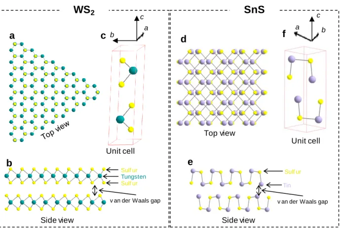
2.1. Structures of WS2 and SnS
2.1.1. Structures of WS2
WS
2belongs to space group symmetry of P63/mmc. WS
2has two polytypes which
are 2H-WS
2(hexagonal) and 1T-WS
2(distorted). These two polytypes have completely
different electrical properties. Semiconducting properties can be found in 2H-WS
2,and
metallic behavior is observed in 1T-WS
2. Interestingly, the semiconducting 2H-WS
2is the
most stable phase of WS
2that can be found in nature.
1In this thesis, the discussion is
limited to 2H-WS
2as it is the main focus. In bulk structure, each layer of WS
2is stacked
each other by van der Waals interaction. Figures 2-1a,b illustrate the top and side views
of two-layer WS
2stacked by the van der Waals interaction. Due to this van der Waals
interaction, the coupling between WS
2layers, and quantum confinement, the different
number of layer of WS
2results in different electrical and optical properties which will be
discussed in later. Figure 2-1c presents a unit cell of WS
2with the lattice parameters of a
= b = 3.154 Å and c = 12.364 Å.
22.1.2. Structure of SnS
Tin sulfide is a compound that can exist in different polymorphs. The different oxidation number of Sn makes tin sulfide exists in three different polymorphs: SnS, SnS
2, and Sn
2S
3. Moreover, SnS itself has three different polytypes that belong to different space group symmetry: Pnma, Fm3m, and Cmcm. SnS with Pnma structure is the most stable phase, and other phases can be obtained at higher deposition temperatures of 700
°C and 1000 °C.
3The Pnma is orthorhombic symmetry which shows large anisotropic behavior between the zig-zag and the armchair edge, where the top and side views of SnS
Figure 2-1. Atomic models of top and side view of (a,b) WS2 and (d,e) SnS. Schematic view of a unit cell of (c) WS2 and (f) SnS.
a b
c
Sulf ur Tungsten Sulf ur v an der Waals gap
a c
b
Side view
Unit cell
Unit cell
a b
c
f
Tin Sulf ur
v an der Waals gap
Side view Top view
d
e
SnS
WS
2are given in Figures 2-1d,e.
4Moreover, the symmetry breaking of this phase and flexible structure of SnS generate a giant piezoelectric coefficient in SnS.
5Having similar layered structured with WS
2, each layer of SnS is also stacked together by van der Waals interactions. However, the van der Waals interaction of each layer of metal chalcogenides (i.e., SnS and SnSs) is very strong and makes it difficult to form single-layer structure of SnS.
6,7Until now; there is no report on properties of single-layer SnS, because the isolation of single-layer SnS is still difficult to be obtained. Figure 2-1f shows one unit cell of SnS with the lattice parameters of a = 4.334, b = 3.987, and c = 11.199.
82.1.3. Phonon modes of WS
2and SnS
In order to analyze atomically thin materials, advanced characterization apparatuses with nanometer-scale resolutions are needed. TEM has the ability to observe
Figure 2-2. a) Schematic view of Raman modes of WS2. Typical Raman spectra of single-layer WS2 collected with excitation wavelength of (b) 514 and (c) 488 nm. d) Peak frequencies of A1g, E12g, and 2LA vibrational modes as a function of number of WS2 layers. Figures b,c are reproduced from Ref. 11
E22g E1g E12g A1g
a
b
d c
each atom arrangement in 2D materials. Furthermore, the TEM apparatus equipped with energy-dispersive X-ray spectroscopy (EDS) module can determine what kind of atoms are existing in the 2D materials.
9However, these methods are time-consuming and destructive to the sample. A fast and non-destructive characterization is needed to confirm the presence of 2D materials. Phonon modes studies could give insight into the presence of 2D materials, especially Raman spectroscopy. Since the different 2D material has unique Raman fingerprint, Raman spectroscopy becomes a powerful tool in 2D material characterization. In this thesis, the main characterization to confirm the presences of 2D materials is based on Raman spectroscopy. Therefore, the short introduction to the phonon modes of WS
2and SnS is given in this section.
2.1.3.1. Phonon modes of WS2
2H-WS
2has four vibrational modes that can be detected by Raman spectroscopy, which assigned to A
1gand E
12g, E
22g, and E
1gmodes.
10These vibrational modes are
Figure 2-3. a) Schematic view of Raman vibrations of SnS. b) Typical Raman spectra of SnS with different thickness. Figure b is reproduced from Ref. 13.
A
g(40 cm
-1) A
g(96 cm
-1) A
g(192 cm
-1)
A
g(219 cm
-1) B
3g(49 cm
-1) B
3g(164 cm
-1)
a b
depicted in Figure 2-2a. A
1gmode is out-plane atomic displacement that can be detected at Raman shift of 417 cm
-1. Next, at Raman shift of 356 cm
-1, the E
12g, in-plane atomic displacement, also can be detected.
11Since these two peaks gives strong Raman intensity, these two modes are usually used to confirm the existence of WS
2among other Raman peaks. Another peak called 2LA is originated from the double resonant scattering, which is only detected by green excitation source.
11Another interesting point is that the peak positions of A
1gand E
12gstrongly depend on the number of WS
2layers, as shown in Figure 2-2d. The frequency separation of A
1gand E
12gis often used for determination of the number of layers of WS
2.
2.1.3.2. Phonon modes of SnS
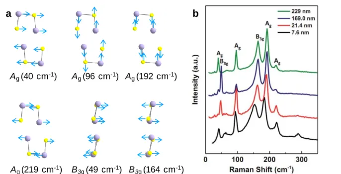
There exist 21 vibrational modes in SnS.
12Among these vibrational modes, only two vibrational modes show intense peaks strong enough to be detected by the confocal Raman spectroscopy.
4These Raman modes are known as A
gand B
3gwhich are illustrated in Figure 2-3a. Moreover, the Raman intensity of SnS also behaves similarly to WS
2where the larger number of layers of SnS gives more intense Raman intensity. Figure 2-3b shows an example of Raman spectra of SnS with different thickness.
132.2. Electrical properties of WS
2and SnS
In this section, the electrical properties of WS
2and SnS from theoritical point of
view will be described. This introductory is expected to give some insight how the
electronic devices based on WS
2or SnS perform. Then, the summaries of previous work
on empirical electrical properties of WS
2and SnS will be given in Chapter 3.
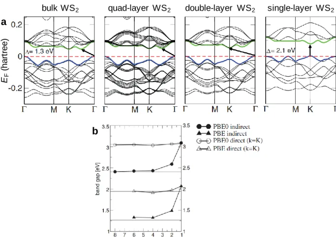
2.2.1. Band structures of WS
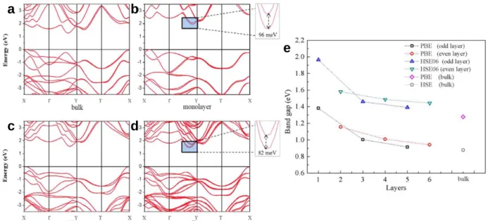
2and SnS
The band structure of single-layer WS
2and those of larger number of layers are shown in Figure 2-4a. First, the discussion of the band gap evolution of WS
2will be described. Interestingly, it can be seen that the indirect band gap of WS
2becomes wider with the decreasing the number of WS
2layers.
14On the other hand, the direct band gap of WS
2remains unchanged with different thickness, as can be seen in Figure 2-4b.
14Eventually, at the single-layer form, the indirect band gap of WS
2becomes larger than its direct band gap and the natural band gap of single-layer WS
2changes from indirect to direct. This evolution is very beneficial, because the direct bandgap semiconductor is preferable in optoelectronic applications. Theoretical result is consistent with result
Figure 2-4. a) Band structures of bulk, quad-, double-, and single-layer WS2 calculated by DFT/PBE simulation.
b) Calculated indirect and direct band gap of different number (N) of WS2 layers. Circles and triangles data sets show the result with different calculation methods. Reproduced from Ref. 14.
E
F(h a rt re e )
bulk WS
2quad-layer WS
2double-layer WS
2single-layer WS
2a
b
obtained by photoluminescence spectroscopy. Since the direct band semiconductor emits strong photoluminescence, one can distinguish the presence of single- and double- layer WS
2just by examining their PL intensities.
15The photoluminescence of double- layer WS
2is much lower than its single-layer form, originating from the indirect band gap of double-layer WS
2.
Next, the band structure of SnS with different number of layers is summarized.
The band gap evolution of SnS also shows a similar trend with WS
2, where the SnS band gap increases as the number of layer decreases, as shown in Figures 2-5a-d.
16In bulk SnS, the band gap is predicted to be ~1.2 eV. The band gap gradually increases to 1.9 eV for the single-layer case.
16However, the indirect-to-direct band gap transition, which is observed in single-layer WS
2, is absent in the SnS case. SnS is indirect band gap irrespective of the number of layers. Moreover, the most interesting point is that the band gap evolution of SnS is also influenced by the odd/even number of layer of SnS (Figure 2-
Figure 2-5. a-d) Band structures of (a) bulk, (b) triple-, (c) double-, and (d) single-layer SnS calculated by DFT simulation. b) Calculated band gap of odd-even number of SnS layers with different approximation methods.
Reproduced from Ref. 14.
a b
d c
e
5e)
16. It is predicted that the even-numbered layer of SnS has a larger band gap compared with the odd-numbered layer. Moreover, due to high asymmetric structures of odd- numbered layer of SnS, the SnS with an odd number of layer will be having a giant band- splitting of more than 80 meV (see Figures 2-4b,d).
16This value is very high compared with other MCs and TMDCs, makiing SnS as a promising material for spintronic applications.
2.2.2. Expected carrier mobility of WS
2and SnS
For predicting the field effect carrier mobility of 2D materials, the Takagi model promises a better approximation because it evaluates from 2-dimensional electron gas point of view than other carrier mobility simulations.
17At first, this method was used to calculate the carrier mobility of Si with different crystal orientations, and it agreed well with the experimental data. However, recently, it becomes popular to approximate the carrier mobility in 2D materials such as antimonene, fluorinated graphene, and phosphorene.
18–20Thus, the expected carrier mobility of WS
2and SnS by using Takagi model are summarized in this section. The Takagi model used for calculating carrier mobility of 2D material (μ
2D) can be written as:
𝜇
2D=
𝑒ℏ3𝐶2D𝑘b𝑇𝑚e∗𝑚d(𝐸l𝑖)2
(2-1)
where 𝑚
e∗is the effective carrier (electron or hole) mass along the transport direction and
𝑚
d= √𝑚
x∗𝑚
y∗is the average density-of-state mass. The deformation potential and elastic
modulus of the longitudinal acoustic mode are defined as 𝐸
l𝑖and C
2D, respectively. The e,
k
b, T and ℏ are elementary charge, Boltzmann’s constant, temperature, and reduced
Plank’s constant, respectively.
Equation 2-1 shows that the carrier mobility of 2D materials is inversely proportional to the effective carrier mass of the materials, which is similar to the mobility and effective carrier mass relation in 3D materials. Table 2-1 shows the comparison of effective carrier mass of WS
2and SnS and their carrier mobilities.
16,21Furthermore, the calculation result of well-known MoS
2(for WS
2comparison) and SnSe (for SnS comparison) are also given.
21,22The mobility of WS
2is much higher than the mobility of MoS
2, because the effective mass of electrons in WS
2is lighter than MoS
2. In SnS and SnSe case, SnS is predicted to have higher carrier mobility than SnSe. Even though the effective mass of SnS is heavier than one in SnSe, the deformation potential of SnS (9.2 eV) is much smaller than that of SnSe (3.9 eV).
16,22Thus, considering the factor of deformation potential ( 𝐸
l𝑖) of equation 2-1, smaller deformation potential likely promotes higher carrier mobility, because the deformation potential is inversely proportional to the carrier mobility.
However, the calculated mobility values here are overestimated than the values that are observed experimentally. There are several factors that needed to be considered.
Table 2-1. Expected carrier mobility of WS2, MoS2, SnS, and SnSe. The data were obtained from ref. 16, 21, and 22.
Material
Effective electron mass me (m0)
Effective hole mass mh (m0)
Electron mobility
μe (cm2/Vs) Hole mobility μh (cm2/Vs)
WS2 0.24 1,103
MoS2 0.45 340
SnS 0.22 10,000
SnSe 0.13 723
First, the intrinsic factors such as impurities, defects, and phonon scattering that can be described by Matthiessen rule, (
1𝜇
=
1𝜇impurity
+
1𝜇lattices
+
1𝜇defects
+ ⋯ ) , are needed to be considered.
23Next, the extrinsic factors might also alter the mobility. For example, the rough substrates or humidity could degrade also the carrier mobility of 2D materials.
24Therefore, the review of mobility values and device performance based on experimental data will be described further in Chapter 3.
2.3. Material preparation: CVD growth of TMDCs, MCs, and 2D materials-based heterostructures
CVD is the best method to synthesize high-quality 2D materials in large area up to
now. The development of CVD method of TMDCs is very decent, resulting a lot of
publications in last several years. The simplest way to obtain good TMDCs is to use
transition metal oxide (WO
3and MoO
3) and solid chalcogenide (S, Se) as the precursors,
because the solid precursors are easy to handle. The first demonstration of CVD growth
of transition metal dichalcogenides (TMDCs) was done by Lee et al. in 2012.
25They
heated up the MoO
3,and sulfur powder at an elevated temperature of 650 °C and the
resulted MoS
2grains with lateral size of ~50 μm were deposited on SiO
2substrates, as
shown in Figures 2-6a,b. The first report on CVD growth of WS
2was recorded in 2013 by
Zhang et al.
26The method to grow WS
2is almost similar to MoS
2growth. The main
difference is that WO
3precursor is needed to be heated up to 900 °C due to its high
melting point. The lateral size of WS
2made by using this method was around ~50 μm, as
shown in scanning electron microscopy (SEM) image in Figures 2-6c,d.
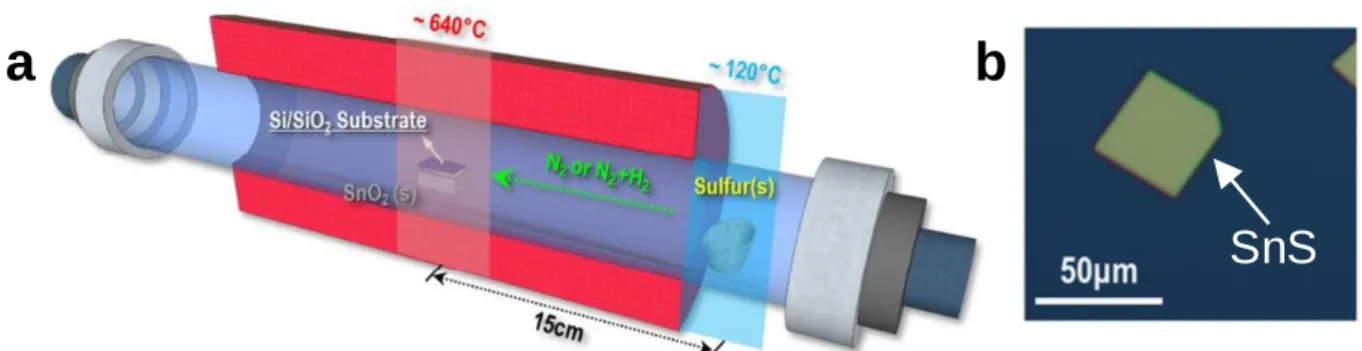
The studies on metal chalcogenides (MCs) growth, especially SnS, are gaining interest just recently. The first report of SnS growth by CVD was published in 2015.
27Again, the method is almost similar to TMDCs growth, which SnO
2and solid sulfur precursor were used as feedstock. As shown in Figure 2-7a, the SnO
2and sulfur
Figure 2-6. a) Schematic view of MoS2 CVD setup and (b) optical image MoS2 grains on SiO2 substrate. c) Schematic view of WS2 CVD setup and (d) SEM image of a WS2 grain on sapphire substrate. Figures a and b are reproduced from Ref. 25. Figures c and d are reproduced from Ref. 26
a MoS
2c WS
2MoS
2MoS
2b d
Figure 2-7. a) Schematic view of CVD setup for SnS growth and (b) optical image SnS grain on SiO2 substrate.
Reproduced from ref. 27
SnS
a b
precursors were heated inside a quartz tube to 640 °C and 120 °C independently. The resulted SnS grain shown n Figure 2-7b has square shape with lateral size of ~50 μm, reflecting its rhombohedral structure.
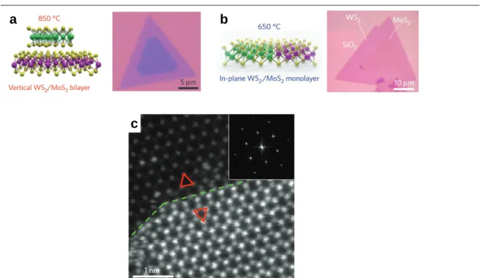
Various kinds of 2D materials-based heterostructure can be also synthesized by CVD method, opening the opportunity in large-scale production. The first report on 2D materials-based heterostructures can be found in 2014.
28The vertical and in-plane heterostructures of MoS
2and WS
2were achieved by changing the growth temperatures, as shown in Figures 2-8a,b. The sharp interface between MoS
2and WS
2, shown in TEM image in Figure 2-8c, is the main advantage over the heterostructure fabricated by exfoliation method. Another approach to achieved different heterostructure is by using two-step CVD. For example, the heterostructure of graphene-MoS
2and PbS-MoS
2have been reported by the two-step CVD.
29,30This approach needs two times CVD processes, where the first material was synthesized beforehand. In the graphene-MoS
2case, the
Figure 2-8. Schematic views and optical micrograph images of (a) lateral and (b) in-plane of MoS2 and WS2
heterostructures resulted from different growth temperature. c) TEM images of interface of in-plane MoS2- WS2 heterostructure. Reproduced from Ref. 28
a b
c
graphene was grown firstly.
29Then, the synthesized graphene was advanced into different CVD furnace system to growth the MoS
2, resulting in graphene-MoS
2heterostructure. This two-step CVD approach can avoid the formation of transition metal alloy of TMDCs (Mo
xW
1-xS
2) or contamination which can occur when both MoO
3and WO
3precursors are used in one CVD batch.
References
1. Leong, S. X. et al. 2H → 1T Phase Change in Direct Synthesis of WS
2Nanosheets via Solution-Based Electrochemical Exfoliation and Their Catalytic Properties. ACS Appl.
Mater. Interfaces 9, 26350–26356 (2017).
2. Wilson, J. A. & Yoffe, A. D. The Transition Metal Dichalcogenides Discussion and Interpretation of The Observed Optical, Electrical and Structural Properties. Adv.
Phys. 18, 193–335 (1969).
3. Burton, L. A. & Walsh, A. Phase Stability of the Earth-Abundant Tin Sulfides SnS, SnS
2, and Sn
2S
3. J. Phys. Chem. C 116, 24262–24267 (2012).
4. Xia, J. et al. Physical Vapor Deposition Synthesis of Two-Dimensional Orthorhombic SnS Flakes with Strong Angle/temperature-dependent Raman responses. Nanoscale 8, 2063–2070 (2016).
5. Fei, R., Li, W., Li, J. & Yang, L. Giant Piezoelectricity of Monolayer Group IV
Monochalcogenides: SnSe, SnS, GeSe, and GeS. Appl. Phys. Lett. 107, 173104 (2015).
6. Qin, G. et al. Diverse Anisotropy of Phonon Transport in Two-dimensional Group IV–
VI Compounds: A Comparative Study. Nanoscale 8, 11306–11319 (2016).
7. Zhang, L.-C. et al. Tinselenidene: A Two-dimensional Auxetic Material with Ultralow Lattice Thermal Conductivity and Ultrahigh Hole Mobility. Sci. Rep. 6, 19830 (2016).
8. Ehm, L. et al. Pressure-induced Structural Phase Transition in The IV–VI Semiconductor SnS. J. Phys. Condens. Matter 16, 3545 (2004).
9. Haigh, S. J. et al. Cross-sectional Imaging of Individual Layers and Buried Interfaces
of Graphene-based Heterostructures and Superlattices. Nat. Mater. 11, 764 (2012).
10. Zhang, X. et al. Phonon and Raman Scattering of Two-dimensional Transition Metal Dichalcogenides from Monolayer, Multilayer to Bulk Material. Chem. Soc. Rev. 44, 2757–2785 (2015).
11. Berkdemir, A. et al. Identification of Individual and Few Layers of WS
2using Raman Spectroscopy. Sci. Rep. 3, 1755 (2013).
12. Chandrasekhar, H. R., Humphreys, R. G., Zwick, U. & Cardona, M. Infrared and Raman Spectra of The IV-VI Compounds SnS and SnSe. Phys. Rev. B 15, 2177–2183 (1977).
13. Li, M. et al. Revealing Anisotropy and Thickness Dependence of Raman Spectra for SnS Flakes. RSC Adv. 7, 48759–48765 (2017).
14. Kuc, A., Zibouche, N. & Heine, T. Influence of Quantum Confinement on The Electronic Structure of The Transition Metal Sulfide TS
2. Phys. Rev. B 83, 245213 (2011).
15. Gutiérrez, H. R. et al. Extraordinary Room-Temperature Photoluminescence in Triangular WS
2Monolayers. Nano Lett. 13, 3447–3454 (2013).
16. Xin, C. et al. Few-Layer Tin Sulfide: A New Black-Phosphorus-Analogue 2D Material with a Sizeable Band Gap, Odd–Even Quantum Confinement Effect, and High Carrier Mobility. J. Phys. Chem. C 120, 22663–22669 (2016).
17. Takagi, S., Toriumi, A., Iwase, M. & Tango, H. On The Universality of Inversion Layer Mobility in Si MOSFET’s: Part II-effects of Surface Orientation. IEEE Trans. Electron Devices 41, 2363–2368 (1994).
18. Pizzi, G. et al. Performance of Arsenene and Antimonene Double-gate MOSFETs from
First Principles. Nat. Commun. 7, 12585 (2016).
19. Bruzzone, S. & Fiori, G. Ab-initio Simulations of Deformation Potentials and Electron Mobility in Chemically Modified Graphene and Two-Dimensional Hexagonal Boron- nitride. Appl. Phys. Lett. 99, 222108 (2011).
20. Qiao, J., Kong, X., Hu, Z.-X., Yang, F. & Ji, W. High-Mobility Transport Anisotropy and Linear Dichroism in Few-layer Black Phosphorus. Nat. Commun. 5, 4475 (2014).
21. Zhang, W., Huang, Z., Zhang, W. & Li, Y. Two-Dimensional Semiconductors with Possible High Room Temperature Mobility. Nano Res. 7, 1731–1737 (2014).
22. Zhou, M., Chen, X., Li, M. & Du, A. Widely Tunable and Anisotropic Charge Carrier Mobility in Monolayer Tin(ii) Selenide Using Biaxial Strain: A First-principles Study.
J. Mater. Chem. C 5, 1247–1254 (2017).
23. Sze, S. M. & Ng, K. K. Physics of Semiconductor Devices. (Wiley-Interscience, 2007).
24. Chhowalla, M., Jena, D. & Zhang, H. Two-Dimensional Semiconductors for Transistors. Nat. Rev. Mater. 1, natrevmats201652 (2016).
25. Lee, Y.-H. et al. Synthesis of Large-Area MoS
2Atomic Layers with Chemical Vapor Deposition. Adv. Mater. 24, 2320–2325 (2012).
26. Zhang, Y. et al. Controlled Growth of High-Quality Monolayer WS
2Layers on Sapphire and Imaging Its Grain Boundary. ACS Nano 7, 8963–8971 (2013).
27. Ahn, J.-H. et al. Deterministic Two-Dimensional Polymorphism Growth of Hexagonal n-Type SnS
2and Orthorhombic p-Type SnS Crystals. Nano Lett. 15, 3703–3708 (2015).
28. Gong, Y. et al. Vertical and In-plane Heterostructures from WS
2/MoS
2Monolayers.
Nat. Mater. 13, 1135–1142 (2014).
29. Roy, K. et al. Graphene-MoS
2Hybrid Structures for Multifunctional Photoresponsive
Memory Devices. Nat. Nanotechnol. 8, 826–830 (2013).
30. Wen, Y. et al. Integrated High-Performance Infrared Phototransistor Arrays
Composed of Nonlayered PbS–MoS
2Heterostructures with Edge Contacts. Nano Lett.
16, 6437–6444 (2016).
This page is intentionally left blank.
Chapter 3
2D Materials-Based Field-Effect Transistors
3.1. Field-effect transistor operation
Complementary metal oxide semiconductor (CMOS) is the heart of electronic
devices. CMOS consists of two different polarities (p- and n-) field-effect transistors
(FETs) that can be switched on and off.
1The active materials of FETs are semiconductors
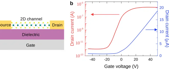
whose conductivity can be tuned by using external electric field. Figures 3-1a shows a
schematic view of 2D-based FETs, where WS
2is chosen as semiconductor for the
definitive purpose. The FET operation in 2D materials is more or less similar to that seen
in 3D materials. This FET consists of 4 main components: source, drain, channel, and
dielectric gate.
2Source and drain are connected by 2D semiconductor that acts as a
channel. The conductance of the semiconducting channel that can be altered by using
and electric field induced by the gate. The higher conductance of semiconducting channel leads to higher drain-source current value (I
DS), while lower conductance will give a lower I
DSvalue.
Now, the on-off operation of n-type FET is described.
3Figure 3-1b shows typical I
DS-V
GScurves in linear and logarithmic scale (transfer curve) of n-type FET. When the gate is applied with a positive voltage, the FET is considered at the on-state. The I
DSvalue is high due to high conductance of the channel, because the Fermi-level of semiconductor moves to its conduction band edge. The Fermi-level transition is originated in the gate- induced electric-field, which is applied by a positive voltage. When the gate voltage is not applied, the FET is at off-state, because the drain-source current cannot flow in the 2D channel due to low conductance of the channel. The low conductance of the channel is caused by the position Fermi-level of semiconducting channel located far below from its conduction band edge. The on-off operation of p-type FET is vice versa with n-type FET
Figure 3-1. (a) Schematic view of 2D material-based FET device. (b) Typical transfer curve of a conventional n-type FET device. Red and blue curves show logarithmic and linear scales.
Source Drain
Dielectric Gate 2D channel
a
b
-40 -20 0 20 40
10-13 10-11 10-9 10-7 10-5
Drain cur re nt (A)
Gate voltage (V)
0 5 10 15 20
Drain cur re nt ( A)
operation where the applied negative voltage on gate makes conductance of p-type semiconducting channel higher.
To evaluate the FET performance, three factors need to be considered. First, the on-off ratio, a ratio between drain current at on- and off- states, must be between 10
4and 10
7in order to supply the demand in real life applications.
4Second, the high carrier mobility is preferable to achieve high performance FET.
4The carrier mobility (µ) of FET can be extracted from the I
DS-V
GScurve shown in Figure 3-1b by using the following expression:
𝜇 =
𝐿ch𝑔m𝑊ch𝐶g𝑉DS
(3-1)
where g
m=dI
DS/dV
GSis transconductance (can be derived from I
DS-V
GScurve linear scale), L
chis the channel length, W
chis the channel width, C
gis the gate capacitance, and V
DSis the drain voltage. Third, the smallest subthreshold swing parameter (the sensitivity of drain current by the gate voltage), S = dV
GS/d(logI
DS), is required to obtain the low power operation.
4,53.2. WS
2-and SnS-based FET
Here the example from ref. 6 is chosen, because it is one of the earliest report on
WS
2-based FET. Figure 3-2a shows a schematic view of single-layer WS
2FET. The
transfer curves given in Figure 3-2b show that the on-off ratios of WS
2reach 10
6in a
vacuum environment and after annealing treatment. The high on-off ratio of WS
2is
originated from its large band gap of ~2 eV. It is worthy to note that the drain current is
low when the measurement was done in low vacuum or in ambient environment.
Generally, the WS
2FET tends to show n-type behavior. Even though it was predicted as ambipolar semiconductor, the high amount of sulfur vacancies makes WS
2behave as an n-type semiconductor.
6The drain current degradation suggests that the WS
2is very sensitive to the measurement environment. The increased carrier mobility of WS
2at the lower temperature shown in Figure 3-2c indicates that the phonon scattering limits the mobility in WS
2. This mobility is very low compared to its prediction shown in Chapter 2. Several attempts have been studied to improve the carrier mobility in WS
2by using contact engineering or dielectric encapsulation.
7,8For example, the WS
2mobility increased from 163 cm
2/Vs to 214 cm
2/Vs after encapsulation by h-BN layers.
8The
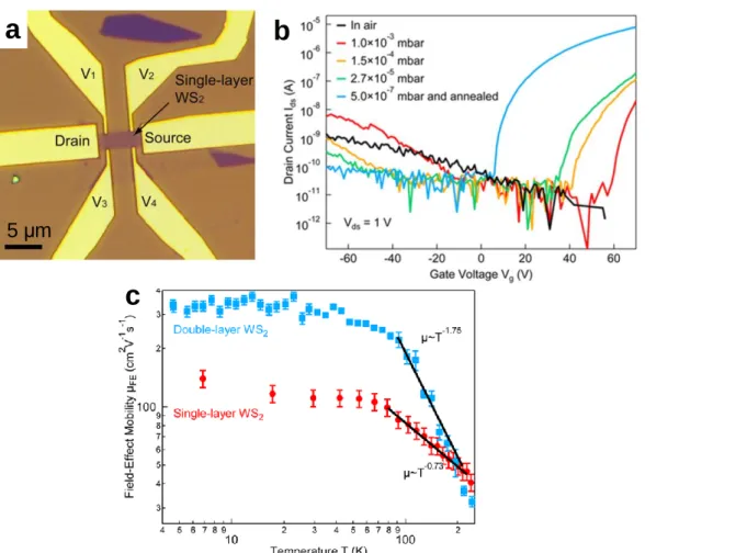
Figure 3-2. (a) Optical micrograph of single-layer WS2 FET device. (b) Transfer curves of the single-layer WS2 under different environment. (c) Field-effect mobility as a function of temperature. Reproduced from Ref. 6.
a
5 μm
b
c
subthreshold swing parameter (S) could be also improved by the ionic liquid which produce a large electric field. Jo et al. demonstrated the very low subthreshold swing parameter of <60 meV by using gating with one of ionic liquid (Diethylmethyl (2- methoxyethyl) ammonium bis (trifluoromethylsulfonyl) imide).
9In Chapter 4, the improvement of WS
2carrier mobility by the contact engineering will be described.
Different from WS
2, the report on SnS FET is quite scarce. Until now, there are only three reports that have reported SnS FET so far.
10–12The reason might be because the SnS does not show good gate dependence, indicating that the SnS FET device cannot be turned off at room temperature. There are two possible reasons why the SnS FET cannot be turned off. First, the high degree of tin vacancy in SnS generates a large amount of hole concentration (10
19cm
-3), resulting in metallic-like behavior.
13Second, the large number of SnS layers screen the electric field applied from the gate, resulting in small gate dependency.
14Figures 3-3a shows p-type transfer curves of thin SnS FET (~12 nm) measured at different temperatures. This thin SnS was turned off at low temperature.
Figure 3-3. (a) Optical micrograph of single-layer FET device. (b) Transfer curves of single-layer WS2 under different environment. (c) Field-effect mobility as function of temperature. Reproduced from Ref. 10.