Tunable Graphene Lateral Tunnel Diodes
著者
Kanako Shiga, Takahiro Komiyama, Yoshiki Fuse,
Hirokazu Fukidome, Akira Sato, Taiichi Otsuji,
Takashi Uchino
journal or
publication title
Japanese Journal of Applied Physics
volume
59
page range
SIID03-1-SIID03-6
year
2020-04-13
URL
http://hdl.handle.net/10097/00131509
Electrical Transport Properties of Gate Tunable Graphene Lateral
Tunnel Diodes
Kanako Shiga1, Takahiro Komiyama2, Yoshiki Fuse2, Hirokazu Fukidome2, Akira Sato2, Taiichi Otsuji2, and Takashi Uchino1*
1
Dept. of Electrical and Electronic Engineering, Tohoku Institute of Technology, Sendai, Miyagi 982-8577, Japan
2
RIEC, Tohoku University, Sendai, Miyagi 980-8577, Japan
E-mail: [email protected]
A detailed study of the electrical transport properties of gate tunable graphene lateral tunnel diodes is presented. The graphene-Al2O3-graphene lateral tunnel diodes are
fabricated on Si/ SiO2 substrates, and the fabricated devices show rectifying characteristics
at the low voltage below 1 V. The rectifying behavior can be controlled by applying back gate voltages. As a result, the devices show high asymmetry and strong nonlinearity current-voltage (I-V) characteristics, which are desirable properties for applications such as optical rectennas and infrared detectors. The electrical transport mechanism of the graphene lateral diodes is analyzed by extracting parameters from the measured I-V characteristics. We find that trap-assisted tunneling from the defect levels in the Al2O3
layer is the most likely mechanism of the forward current of the fabricated graphene lateral diodes.
1. Introduction
Low dimensional materials have attracted attention in recent years because of their excellent electrical properties and might enable innovative architectures in the ‘More than Moore’ and ‘Beyond-CMOS’ domains where add functionalities to nanodevices.1-3) In particular, graphene is one of the most attractive building blocks due to its excellent electronic, optical, mechanical, and chemical properties. Graphene has spurred research into many novel applications including high-frequency devices, biosensors, optical devices.4-7) For example, the vertical graphene junction has been studied for tunneling and terahertz emission devices.8-11) As for the photovoltaic devices, a high performance graphene/MoS2/Si Schottky junction solar cell with power conversion efficiency around
16% has been reported.12) Schottky junction solar cells with transparent two-dimensional materials have an advantage over traditional p-n junction solar cells due to ease of fabrication, their cost, and flexible device applications. However, the power conversion efficiency of Schottky junction solar cells is not high enough to take over the p-n junction solar cells.
Recently, optical rectenna based on carbon nanotubes (CNTs) has been demonstrated as an alternative energy harvesting device.13) The optical rectenna is composed of an ultra-high-speed diode and a nanoscale antenna, which is small enough to couple optical solar radiation. R. L. Bailey first proposed the concept of optical rectenna in 1972.14) However, it could not be realized until the nanofabrication techniques were established. In this device, the nanoscale antenna receives the incoming radiation, and the adjacent diode converts the AC signal into DC voltage. The prospective conversion efficiency of the optical rectenna is about two times higher than the theoretical efficiency of single-junction solar cells.15) While optical rectenna has advantages over semiconducting photovoltaics, the reported conversion efficiency of this device is less than 0.1%.16) Consequently there is still room for improvement in terms of device structures and materials. Thin film metal-insulator-metal (MIM) tunnel diodes are one of the most promising devices for optical rectennas, which require ultra-high-speed operation over 100 THz. A simple structure of MIM tunnel diode can reduce parasitic capacitance and switching time due to the use of tunneling current between metal electrodes separated by a thin insulating film. The critical issue in the optical rectenna is impedance matching between the antenna and diodes to maximize the power transfer. To improve impedance mismatch, a device structure whose nanoscale antenna merged with MIM tunnel diode together was proposed.17) Another issue that needs to be tackled is that optical rectennas require high
performance MIM tunnel diodes, which have highly asymmetric I–V characteristics and a reasonable degree of nonlinearity.
In this study, a detailed investigation of graphene-insulator-graphene (GIG) lateral tunnel diodes is carried out to explore the potentiality of graphene applications. We develop device fabrication processes and investigate the electrical transport properties of the fabricated devices. As the GIG lateral tunnel diodes show symmetric I-V characteristics due to the same electrode material, the external bias is needed to produce asymmetric I-V curves. Thus this work aims at developing GIG lateral tunnel diodes with the asymmetry I-V curves. The back gate structure is applied to the graphene tunnel diodes to modify the I-V characteristics. Finally, measured I-V characteristics, including temperature dependence, are analyzed to clear the transport mechanism in the GIG lateral tunnel diodes.
2. Experimental methods
Figure 1 shows schematic cross-sectional and top views of the fabricated device. We used commercially available monolayer chemical vapor deposition (CVD) graphene films (Graphene Supermarket) as the starting material, which were grown by CVD on Cu foils and transferred on Si/ SiO2 substrates later on. The measured Raman spectra indicate that
graphene film is single-layer and low defect density.18) We prepared two samples with different tunnel dielectric structure (Table I) to investigate the transport mechanism in the fabricated diodes. Before starting the device fabrication, the as-received substrates were annealed at 350 °C for 1 hour in Ar to prevent the graphene from peeling off from the SiO2
surface. Then, graphene was covered with a 6-nm-thick Al2O3 layer formed by natural
oxidation of Al thin film. The Al2O3 passivation layer was introduced to protect the
graphene surface from the contamination caused by photoresist during the device fabrication process. The active regions of devices were formed by a combination of photolithography and reactive ion etching (RIE) of oxygen at 100 W for 2 mins. Anode and cathode electrodes were formed by electron beam evaporation of Ti/Pd/Au (0.5/20/100 nm) and lift-off. In this process, semicoclean 23 (Furuuchi. Chemical Co.) was used after the development of photoresist for removing the Al2O3 layer on graphene. Next, O2/Ar (17/34
sccm) plasma treatment was carried out at 50 W for 3 seconds just before the deposition of metals to reduce the contact resistance. The additional thin titanium layer improves the adhesion between the graphene and the palladium layer. The tunnel regions in the active area were defined by electron beam lithography, and RIE of oxygen at 100 W for 30
seconds formed the tunnel lengths ranging from 40-220 nm. Tunnel dielectrics consist of two layers (Table I) were deposited on the gap between the adjacent graphene domains to investigate the impact of the plasma-induced damage on the tunnel current. As for device #1, Al2O3 film with a thickness of 20 nm was deposited at 220 °C by using atomic layer
deposition (ALD) after the formation of 6-nm-thick natural Al2O3 layer. As for device #2,
Si3N4 film with a thickness of 16 nm was deposited at 250 °C using plasma-enhanced CVD
(PECVD) after the formation of 14-nm-thick natural Al2O3 layer, which was formed by the
superposition of 7-nm-thick natural Al2O3 films. To open the contact windows for anode
and cathode electrodes, dry and wet etch were employed. Finally, 100-nm-thick aluminum was deposited on the backside of the Si substrate as a back-gate electrode.
The electrical characteristics of the fabricated devices were mainly carried out by using a semiconductor parameter analyzer (Keysight Technologies B1500A). As for the temperature dependence of the electrical transport properties, cryogenic probe station (Lake Shore CRX-4K) and the semiconductor parameter analyzer (Keithley 4200A) were used to measure low temperatures ranging from 50 to 300 K. Field emission scanning electron microscope (FESEM; JEOL JSM-6340F) was used to analyze the device structure.
3. Results and discussion
3.1 Electrical properties of the lateral GIG diodes
Figures 2(a) and (b) show I-V characteristics of the fabricated devices as a function of gate voltage (Vg). The measured results of device #1 with a tunnel length (LT) of 120 nm
and device #2 with LT=40 nm are shown in Figs. 2(a) and 2(b), respectively. Both devices
exhibited the symmetrical rectifying characteristics at a low voltage below 1 V. These I-V curves were shifted horizontally by applying gate voltages. The devices have the positive threshold voltage for the negative gate voltages and the negative threshold voltage for the positive gate voltages. The external gate voltages can improve the asymmetry in the forward characteristics of the GIG diode. The back gate voltage induces an electric field that can electrostatically modulate the work function of graphene.19-21) The work function of undoped graphene is around 4.6 eV, which can be adjusted by the gate voltage. As a result, the modulated the work function of the graphene through the back gate electrode allows changing the threshold voltage of diodes.
A distinct difference between the two devices was on-current. The on-current of device #1 is about three orders of magnitude smaller than that of device #2, which suggests that the on-current is attributed to the tunneling effect.
Figure 3 shows gate current-gate voltage (Ig-Vg) characteristics of the same devices shown in Fig. 2. The insets exhibited the I-V characteristics of the devices at Vg=-0.5 V for comparison. The forward current was larger than the leakage current for both devices. These results suggest that the leakage current between gate and cathode electrodes is not dominant for the forward current. We also checked the quality of graphene and insulating layers using graphene field effect transistors (FETs, Supplementary Information S1-3). The measurement results suggest that both graphene and gate dielectrics are working properly, and the devices have no leakage current. The field effect mobility of graphene was estimated to be 910 cm2/Vs using the graphene FETs, which was comparable with previously reported data.22)
Figure 4 shows the tunnel length (LT) dependence of the tunnel region resistance (RT) to
make clear if the forward current is associated with the tunneling effect. RT was estimated
from the I-V characteristics and exponentially increased with LT, which suggests that the
forward current is attributed to the tunnel effect. The devices #1 and #2 showed the same RT-LT dependence despite the different dielectric structure. This result indicates that the
mechanism of the forward current is same transport mode.
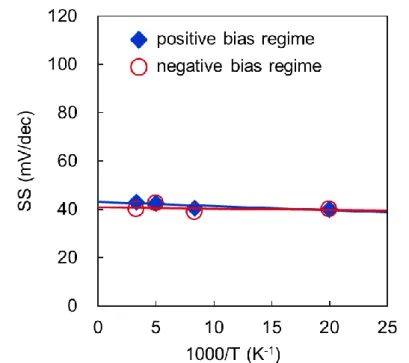
Figure 5 shows the temperature dependence of the I-V characteristics of device #2 to investigate the transport mechanism. The forward current increased with the temperature, but not much. The weak temperature dependence of the I-V characteristics indicates that certain impurity levels are assisted with tunneling transport. The devices also showed a constant subthreshold slope around 40 mV/dec between 50 and 300 K (Supplementary Information S4), which was similar behavior of the MIM diodes. This result indicates that graphene acts as metal due to its semimetal properties.
3.2 Transport mechanism of the lateral GIG tunnel diodes
The transport mechanism of the lateral GIG tunnel diodes were analyzed based on the I-V characteristics. To make clear the current flow path in the device, three paths shown in Fig. 6 were investigated. The direct tunneling of thicker insulator barrier is negligible because of the low electric field. The path A shows the leakage current between the gate and cathode electrodes, the path B shows tunneling current through the dielectrics, and the path C shows the leakage current along with the SiO2/Al2O3 interface, respectively. The
Ig-Vg characteristics in Fig. 3 suggest that gate leakage current (path A) is not associated with the forward current. The measured nonlinear I-V characteristics also suggest that the forward current is unlikely to pass through the path C. Thus, we focused on the path B in
terms of Fowler-Nordheim (FN) tunneling and Poole-Frenkel (PF) conduction.23-25)
Figure 7 shows the FN plot of device #2 with LT=40 nm. The FN tunneling mode is seen
at high voltage region and the slope in the linear region changed with the applied gate voltages. Figure 8 shows gate voltage dependence of the barrier height ΦB deduced from
the slope of the FN plots. The estimated barrier heights are between 0.5 and 0.7 eV in the negative bias regime and between 0.8 and 1.1 eV in the positive bias regime, respectively. These values are not consistent with the values estimated from the energy band diagrams of our devices, and suggest that some impurity levels are also associated with the transport.26-28) FN tunneling is the process whereby carriers pass through the modified tunnel barrier in a high electric field. As the fabricated devices have tunneling lengths ranging from 40 to 220 nm, the carriers pass through the dielectrics via the impurity levels is a likely path in addition to the tunneling. In the FN tunneling process, the carrier transport only depends on the electric field (E), and has no temperature dependence. In contrast, PF conduction has weak temperature dependent I-V characteristics, because the carriers are assisted to the transport with both the electric field and the thermal effects.
Figure 9 shows the PF plot of device #2 with LT=40 nm. The dielectric constants εr
estimated from the slope of the linear region are 8.8 in the negative bias regime and 7.7 in the positive bias regime, which are in good agreement with that of Al2O3.29) This result
indicates that the current through the Al2O3 layer is dominant for the tunneling, and PF
conduction is also associated with the I-V characteristics. SiO2 has a wide bandgap of 8.8
eV, which is larger than that of Al2O3 (6.4 eV), and SiO2 is an unlikely path for
tunneling.29)
Given that the fabricated devices showed both FN tunneling and PF conduction, we can propose the energy band diagrams as shown in Fig. 10. We found that trap assisted tunneling (TAT) is the most likely mechanism in our devices. The estimated tunnel barrier height indicates that some impurity levels are associated with the tunneling paths and in good agreement with the impurity levels of the oxygen vacancies in Al2O3.30) This result
also supports the weak temperature dependence of the I-V characteristics.
In this study, we investigated the transport mechanism of the graphene lateral diodes, and our next step will be to fabricate optical rectennas using graphene. Compared to silicon FETs and carbon nanotube transistors, graphene transistors show higher cut-off frequencies at the same gate length because of their higher mobility and smaller RC delay.31) Thus the conversion efficiency of graphene optical rectenna is expected to be around 0.1%, which is two orders of magnitude higher than the record using carbon nanotube devices.
4. Conclusions
We have successfully fabricated gate tunable graphene lateral tunnel diodes and found that the devices have the rectifying characteristics at the low voltage below 1 V. The rectifying behavior can be controlled by applying gate voltage. The fabricated devices showed asymmetric I-V characteristics and non-linearity, which optical rectenna requires.
The transport mechanism in the graphene lateral tunnel diodes was investigated in terms of FN tunneling and PF emission. The relative dielectric constant εr from the PF plots is
estimated to be 7.7-8.8, which is in good agreement with εr of Al2O3. Taking into account
all measured results, we conclude that trap-assisted tunneling through the oxide defect levels in Al2O3 is the most likely mechanism of the fabricated graphene lateral tunnel
diodes.
Acknowledgments
This work was carried out under the Cooperative Research Project Program of RIEC, Tohoku University, and NIMS Nanofabrication Platform Project supported by MEXT, Japan, Grant Number JPMXP09F18NM0086. The authors acknowledge Prof. Matsui, the University of Tokyo, for help with low-temperature I-V measurements in the Nanotechnology Platform Project.
References
1) M. Chhowalla, D. Jena, and H. Zhang, Nature Reviews Materials, 1, 16052 (2016). 2) T. Uchino, F. Shimpo, T. Kawashima, G. N. Ayre, D. C. Smith, C. H. de Groot, and P.
Ashburn, Appl. Phys. Lett, 103, 193111 (2013).
3) T. Uchino, G. Ayre, D. C. Smith, J. L. Hutchison, C. H. de Groot and P. Ashburn, Electrochemical Solid-State Lett, 14, K21 (2011).
4) E. Guerriero, P. Pedrinazzi, A. Mansouri, O. Habibpour, M. Winters, N. Rorsman, A. Behnam, E. A. Carrion, A. Pesquera, A. Centeno, A. Zurutuza, E. Pop, H. Zirath, and R. Sordan, Scientific Reports 7, 2419 (2017).
5) D. Tsang, T. Lieberthal, C. Watts, I. Dunlop, S. Ramadan, A. Hernandez, and N. Klein, Scientific Reports 9, 13946 (2019).
6) X. An, F. Liu, Y. J. Jung, and S. Kar, Nano Lett. 13, 909 (2013). 7) T. Mueller, F. Xia, and P. Avouris, Nature Photonics 4, 297 (2010).
8) V. Du, Y. Kimura, M. Tahara, K. Matsui, H. Teratani, Y. Ohno, and M. Nagase, Jpn. J. Appl. Phys. 58, SDDE01 (2019).
9) V. Ryzhii, A. A. Dubinov, V. Y. Aleshkin, M. Ryzhii, and T. Otsuji, Appl. Phys. Lett. 103, 163507 (2013).
10) D. Yadav, S. B. Tombet, T. Watanabe, S. Arnold, V. Ryzhii, and T. Otsuji, 2D Mater. 3, 045009 (2016).
11) L. Britnell, R. V. Gorbachev, A. K. Geim, L. A. Ponomarenko, A. Mishchenko, M. T. Greenaway, T. M. Fromhold, K. S. Novoselov, and L. Eaves, Nat. Commun. 4, 1794 (2013).
12) J. Ma, H. Bai, W. Zhao, Y. Yuan, and K. Zhang, Sol. Energy 160, 76 (2018).
13) A. Sharma, V. Singh, T. L. Bougher, B. A. Cola, Nature Nanotechnology 10, 1027 (2015). 14) R. L. Bailey, J. Engineering for Power 94, 73 (1972).
15) G. M. Moddel and S. Grover, Recent Solar Cells (Springer, New York, 2013).
16) E. C. Anderson, T. L. Bougher, and B. A. Cola, Advanced Electronic Materials 4, 1700446 (2018).
17) M. Dragoman and M. Aldrigo, Appl. Phys. Lett. 109, 113105 (2016).
18) Graphene Supermarket. Available at: https://graphene-supermarket.com/Monolayer- Graphene-on-90-nm-SiO2-Wafer-5-pack.html [Accessed: Aug. 17, 2019].
19) Y. J. Yu, Y. Zhao, S. Ryu, L. E. Brus, K. S. Kim, and P. Kim, Nano Lett. 9, 3430 (2009). 20) H. Yang, J. Heo, S. Park, H. J. Song, D. H. Seo, K. Byun, P. Kim, I. Yoo, H. Chung, and
21) L. Britnell, R. V. Gorbachev, R. Jalil, B. D. Belle, F. Schedin, A. Mishchenko, T. Georgiou, M. I. Katsnelson, L. Eaves, S. V. Morozov, N. M. R. Peres, J. Leist, A. K. Geim, K. S. Novoselov, and L. A. Ponomarenko, Science 335, 947 (2012).
22) J. Tian, A. Katsounaros, D. Smith, and Y. Hao, IEEE Trans. Electron Devices, 62, 3433 (2015).
23) M. Lenzlinger and E. H. Snow, J. Appl. Phys, 40, 278 (1969).
24) S. H. Lee, M. S. Choi, J. Lee, C. H. Ra, X. Liu, E. Hwang, J. H. Choi, J. Zhong, W. Chen, and W. J. Yoo, Appl. Phys. Lett. 104, 053103 (2014).
25) V. D. Lecce, S. Krishnamoorthy, M. Esposto, T.-H. Hung, A. Chini, and. S. Rajan, Electron. Lett. 48, 347 (2012).
26) R. K. Chanana, IOSR J. Appl. Phys. 6, 1 (2014).
27) K. Y. Cheong, J. H. Moon, H. J. Kim, W. Bahng, and N.-K. Kim, J. Appl. Phys. 103, 084113 (2008).
28) J. Aarik, V. Bichevin, I. Jogi, H. Kaambre, M. Laan, and V. Sammelselg, Central European J. Phys. 2, 147 (2004).
29) N. Alimardani, S. W. King, B. L. French, C. Tan, B. P. Lampert, and J. F. Conley, Jr., J. Appl. Phys. 116, 024508 (2014).
30) Z. Guo, F. Ambrosio, F Ambrosio, and A Pasquarello, Appl. Phys. Lett. 109, 062903 (2016).
31) F. Schwierz, Proc. 2011 Int. Symp. on VLSI Technology, Systems and Application (VLSI-TSA), 2011, T15.
Figure Captions
Fig. 1. Schematic diagram of the device structure of the graphene lateral tunnel diode. (a)
Cross-sectional view. (b) Top view. LT and W are the tunnel length and width, respectively.
Fig. 2. Current-Voltage (I-V) characteristics of (a) device #1 with LT=120 nm and (b)
device #2 with LT=40 nm. Current is normalized by the width W.
Fig. 3. Gate current-gate voltage (Ig-Vg) characteristics of (a) device #1 with LT=120 nm
and (b) device #2 with LT=40 nm. The insets show the I-V characteristics at Vg=-0.5 V for
comparison.
Fig. 4. Tunnel length (LT) dependence of the tunnel region resistance (RT) of the graphene
lateral tunnel diodes. RT is estimated from the I-V characteristics at V=0.1 V and Vg=0 V.
Fig. 5. Temperature dependence of the I-V characteristics of device #2 with LT=100 nm.
The measurements were carried out in the range of 50-300 K.
Fig. 6. Schematic diagram of prospective current paths of the graphene lateral tunnel diode.
The path A shows the leakage current between the gate and cathode electrodes, the path B shows the tunneling current through the dielectrics, and the path C shows the leakage current along with the SiO2/Al2O3 interface, respectively.
Fig. 7. Fowler-Nordheim (FN) plots of device #2 with LT=40 nm for various gate voltages.
Fig. 8. Gate voltage (Vg) dependence of the measured tunnel barrier height ΦB. Filled
markers show the results in the positive bias regime, and unfilled markers show the results in the negative bias regime. Triangles and diamonds show the results of device #1 and #2, respectively.
Fig. 9. Poole-Frenkel (PF) plots of device #2 with LT=40 nm. The estimated dielectric
Fig. 10. Schematic illustration of the proposed energy band diagram of the graphene lateral
tunnel diode. The tunneling current passes through the Al2O3 film by trap-assisted
tunneling (TAT). The estimated tunnel barrier height (ΦB) indicates the impurity level of
oxygen vacancies in Al2O3. The work function of graphene can be controlled by applying
Table I. Device structure in the tunnel region.
Device Substrate (SiO2 Thickness) Dielectric 1 (Thickness) Dielectric 2 (Thickness) Tunnel Length LT
#1 P+-Si (285 nm) Naturally oxidized Al2O3 (6 nm) ALD-Al2O3 (20 nm) 120-220 nm
Tunnel Diodes”
Kanako Shiga1, Takahiro Komiyama2, Yoshiki Fuse2, Hirokazu Fukidome2, Akira Sato2, Taiichi Otsuji2, and Takashi Uchino1*
1
Dept. of Electrical and Electronic Engineering, Tohoku Institute of Technology, Sendai, Miyagi 982-8577, Japan
2
RIEC, Tohoku University, Sendai, Miyagi 980-8577, Japan
E-mail: [email protected]
S1. I-V characteristics of the top-gate graphene field effect transistor
Figure S1(a) shows the schematic illustration of the top-gate graphene field effect transistor (device #A), which was fabricated at the same time to examine the quality of the stacked dielectric layers of 16-nm-thick Si3N4 and 14-nm-thick Al2O3. Figure S1(b) shows
the drain current-gate voltage (Id-Vg) characteristics of device #A with a gate length (Lg)
of 10 μm and a width (W) of 3 μm at drain voltages Vd= ±0.1 V. The ambipolar behavior with Dirac point of around -2 V was seen.
Fig. S1 (a) Schematic illustration of the top-gate graphene field effect transistor (device #A). (b) Id-Vg characteristics of device #A.
S2. I-V characteristics of the back-gate graphene field effect transistor
Figure S2(a) shows the schematic illustration of the back-gate graphene field-effect transistors (device #B), which was fabricated at the same time to examine the quality of
1 V was seen.
Fig. S2 (a) Schematic illustration of the back-gate graphene field effect transistor (device #B). (b) Id-Vg characteristics of device #B.
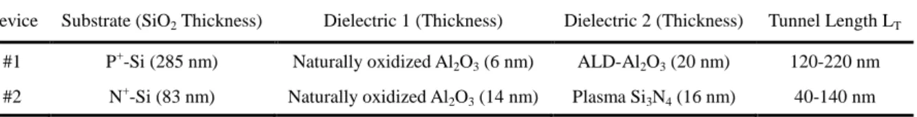
S3. C-V characteristics of graphene field effect transistors
Figure S3 shows typical high-frequency (1 MHz) gate capacitance-gate voltage (C-V) measurement results in both devices #A and #B. The device #A with the stacked dielectric layers of 16-nm-thick Si3N4 and 14-nm-thick Al2O3 showed the distinctive capacitance dip
around -3.0 V, which was corresponding to the charge neutrality point. The gate capacitance of device #B with 83-nm-thick SiO2 was increased with increasing gate
voltage due to the formation of an inversion layer in the Si substrate. The effect of quantum capacitance of graphene can only be seen for thin dielectrics [1], and therefore the quantum capacitance was not observed in device #B.
constant subthreshold slope around 40 mV/dec between 50 and 300 K, which was a similar behavior of the MIM diodes.
Fig. S4 Temperature dependence of the subthreshold slope (SS) of the GIG diode (device #2) with a tunnel length of 140 nm.
Reference