著者 大谷 寿賀子 著者別表示 Otani Sugako journal or
publication title
博士論文要旨Abstract 学位授与番号 13301甲第4319号
学位名 博士(工学)
学位授与年月日 2015‑09‑28
URL http://hdl.handle.net/2297/43857
Creative Commons : 表示 ‑ 非営利 ‑ 改変禁止 http://creativecommons.org/licenses/by‑nc‑nd/3.0/deed.ja
Low power processor architecture and multicore approach for embedded systems 組込み用途向け低消費電力プロセッサ・ア ーキテクチャとマルチコア研究
金沢大学自然科学研究科 電子情報科学専攻
学籍番号( 1323112001 )
氏 名 大谷 寿賀子
Abstract
“ IoT” or “Internet of things” has been absolutely essential to our society and its infrastructures.
Devices are linked to networks from anywhere in the world and will be mutually controlled while information is being exchanged. A microcontroller is one of the important elements of IoT. The microcontroller designers are strongly urged to achieve both high performance computation and low power consumption, which is a hybrid technology with powerfulness of computing and friendliness to the environment.
This thesis focuses on the development of efficient microcontroller architecture for IoT. The basis for the argument is the key of a low power processor architecture is how effective handle on chip memories.
Furthermore, collaboration of software and hardware on multicore architecture can provide dependable and secure networks.
To test our hypothesis, we introduced RX processor core which is suitable for IoT. The RX processor
Instruction set architecture (ISA) and its microarchitecture can achieve lower power consumption and
boost performance. We presented eight-core communication SoC with PCI Express interface. The
multicore SoC can realize a high performance, power-aware, highly dependable network. We also
demonstrated a secure multimedia system by using heterogeneous multicore SoC and software
virtualization.
Chapter 1 Introduction
“IoT” or “Internet of things” formerly known as “ubiquitous computing” has been absolutely essential to our society and its infrastructures. Devices are linked to networks from anywhere in the world and will be mutually controlled while information is being exchanged. A microcontroller is one of the important elements of IoT. The microcontroller designers are strongly urged to achieve both high performance computation and low power consumption, which is a hybrid technology with powerfulness of computing and friendliness to the environment. Furthermore, while network services are gaining popularity, dependability and security of network are more important. A key solution to meet these demands is a compact and low power processor core and multicore technology.
This thesis focuses on the development of efficient microcontroller architecture for IoT. The basis for the argument is the key of a low power processor architecture is how effective handle on chip memories.
Furthermore, collaboration of software and hardware on multicore architecture can provide dependable and secure networks.
1.1 Thesis Contributions
The main contributions of this dissertation are the following:
An RX processor core which is suitable for IoT. The RX processor Instruction set architecture (ISA) and its microarchitecture can achieve lower power consumption and boost performance.
An eight-core communication SoC with PCI Express interface. The multicore SoC can realize a high- performance, power-aware, highly dependable network.
A secure multimedia system that uses heterogeneous multicore SoC and software virtualization.
1.2 Thesis Outline
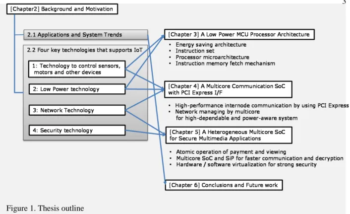
The outline of the remainder of this thesis is as follows.
Chapter 2 provides the background and motivation for this work. It discusses the characteristics and
requirements of IoT by presenting four key IoT technologies.
Chapter 3 introduces t he RX processor core with a low-power processor architecture. The RX processor instruction set architecture (ISA) and its microarchitecture can achieve lower power consumption and boost performance. RXv2 reaches 4.5 Coremark per MHz and the RXv2 processor delivers approximately more than 2.2 – 5.7x the power efficiency of the previous work. The RXv2 processor delivers 1.9 – 3.7x the cycle performance of previous work in digital signal applications.
Chapter 4 presents an eight-core communication SoC with PCI Express interface. PEACH with four PCI Express ports realizes high-performance communication of 4 x 20Gbps and power efficiency of 0.04W/Gbps. The power efficiency of InfiniBand 4X (Commodity network devices) is 0.083W/Gbps.
Thus, PEACH provides 51.5% better power efficiency than InfiniBand 4X. We also evaluate the PEARL network system and demonstrate its fault-tolerant ability.
Chapter 5 demonstrates a secure multimedia system by using a heterogeneous multicore SoC with SiP and software virtualization. The multicore hypervisor virtualizes hardware resources and prohibits operating systems and applications from accessing hardware resources directly.
Finally, Chapter 6 concludes the thesis and suggests directions for future work.
Figure 1. Thesis outline
Chapter 2 Background and Motivation
2.1 Four Key Technologies that support IoT
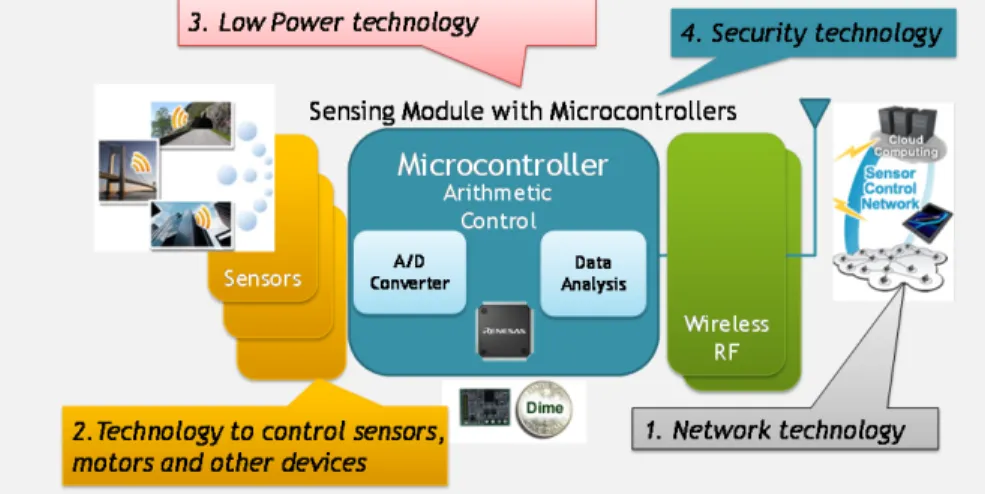
There are four key technologies that supports IoT, 1) network technology to link one device to another, 2) technology to control sensors, motors and other devices, 3) low power consumption technology to raise energy efficiency and 4) security technology (Figure 2).
With an increase in the number of devices on networks, power consumption has become a major issue. Sensing modules must always be active to collect information and be long-lived in infrastructures.
In IoT applications, it is vital to consider how to link applications and microcontrollers, how to communicate for people with electronics devices.
2.2 Research Goals
Given the applications and systems requirements, we consider four key technologies for an efficient microcontroller architecture for
IoT systems:
Network technology
Security technology
Technology to control sensors, motors and other devices
Low-power technology The above features of the architecture and microarchitecture techniques are presented in the following chapters.
Figure 2. Four Key Technologies that support IoT
Chapter 3 Low-Power MCU Processor Architecture
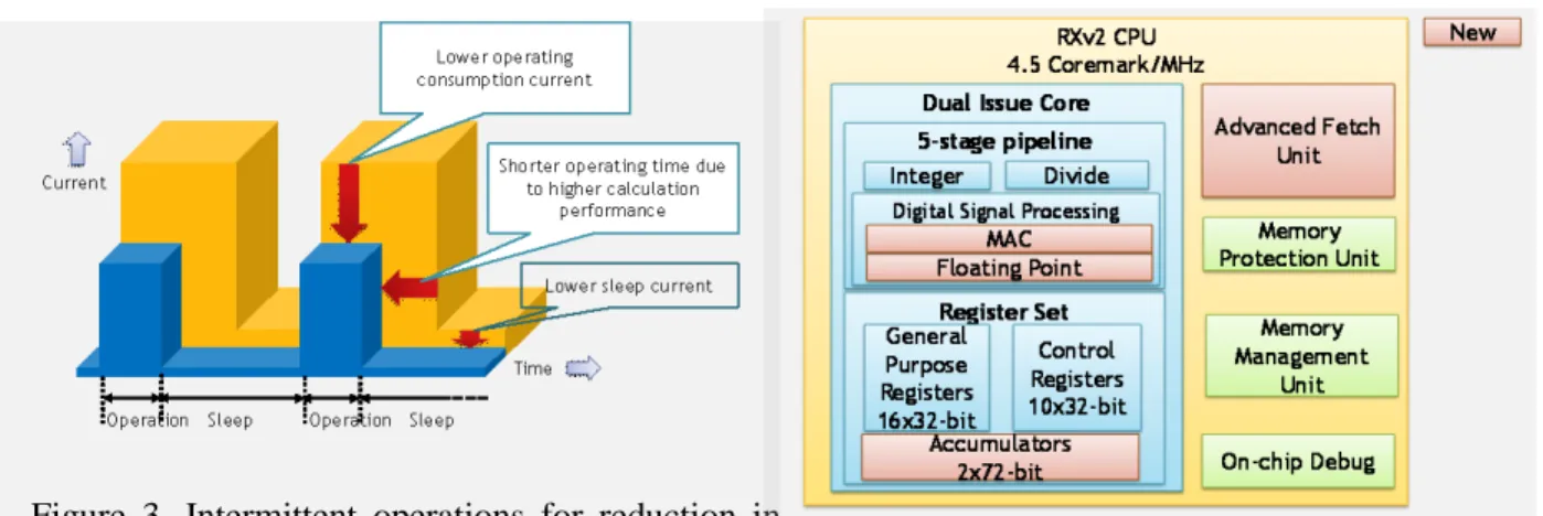
The basic strategy of reducing power consumption is to lower the operating current and shorten the operating time. Figure 3 shows the difference in power consumption of a low-power microcontroller with another microcontroller. The blue bar represents an energy-saving microcontroller with lower operating current and higher performance. The low-power microcontroller completed the same task in much less time, which also enables it to stay in low-power sleep mode longer. This intermittent operations strategy of low-power microcontrollers enables batteries to last a long time.
Design highlights of a low-power processor architecture are instruction set architecture, processor microarchitecture and memory access mechanism. These three items are vital to achieve high performance. Instruction set architecture and memory access mechanisms contribute to low operating current. The most effective way to achieve low operating current is reducing the number of instruction memory accesses, because memories in microcontroller consume a large amount of power.
Application fields of microcontrollers have spread to building automation, medical devices, motor control, e-metering, and home appliances. The demand for such highly intelligent systems has increased.
To meet the demand, the scale and complexity of software has begun to rise. The rapid growth of memory capacity and the advance of microcontroller functions have led to the higher frequency and higher processing performance of embedded
Figure 3. Intermittent operations for reduction in
power consumption Figure 4. RX CPU block diagram
constraints. In order to meet users’ demands for these requirements, we have developed a new RX processor core (RXv2) architecture (Figure 4).
RXv2 is the new generation of RX processor architecture for microcontrollers with high-capacity flash memory. An enhanced instruction set and pipeline structure with an advanced fetch unit (AFU) provide an effective balance between power consumption performance and high processing performance. Enhanced instructions such as the DSP function and floating point operation, and a five- stage dual-issue pipeline synergistically boost the performance of digital signal applications. The RXv2 processor delivers 1.9 – 3.7x the cycle performance of the RXv1 in these applications. The decrease of the number of Flash memory accesses by AFU is a dominant determiner in reducing power consumption. The AFU of RXv2 benefits from adopting a branch target cache, which has a comparatively smaller area than that of a typical cache systems. High code density delivers low power consumption by reducing instruction memory bandwidth. The implementation of RXv2 delivers up to 46% reduction in static code size, and up to 30% reduction in dynamic code size relative to RISC architectures. RXv2 reaches 4.5 Coremark per MHz and operates up to 240MHz. The RXv2 processor delivers approximately more than 2.2 – 5.7x the power efficiency of the RXv1.
The RXv2 microprocessor achieves the best possible computing performance in various applications such as building automation, medical, motor control, e-metering, and home appliances which lead to higher memory capacity, frequency and processing performance.
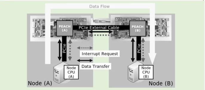
Chapter 4 PEACH: A Multicore Communication SoC with PCI Express I/F
The eight-core communication SoC, code-named “PEACH”, with four 4x PCI Express rev.2.0 ports, realizes a high performance, power-aware, highly dependable network. The network uses PCI Express not only for connecting peripheral devices but also as a communication link between computing nodes.
This approach opens up new possibilities for a wide range of communications. Recent trends in using
computing clusters point to a growing demand for high-compute-density environments in various
application fields such as server appliances including distributed Web servers. Distributed Web servers
need many server nodes and low-latency and high-bandwidth network for operating a massive amount
of Web services, including distribution of high-definition movies. In these computing clusters, power
consumption and system cost have increased. Therefore, it’s vital to downsize computing cluster without losing high dependability, including fault tolerance.
To realize high-performance, power-aware, and highly dependable network, we have proposed a small computing cluster for embedded systems, called PEARL (PCI Express Adaptive and Reliable Link).
Commodity network devices such as Gigabit Ethernet (GbE) and InfiniBand aren’t sufficient for small computing clusters. InfiniBand is a switched fabric communication link used in high-performance computing and enterprise data centers. It achieves high reliability but power consumption is relatively high. GbE is a cost and power rival of InfiniBand. However, GbE does not match InfiniBand’s transmission performance.
To achieve both high performance and low power consumption, PEARL uses PCI Express, a high- speed serial I/O interface standard in PCs, not only for connecting peripheral devices but also as a communication link between computing nodes. To implement PEARL, we’ve developed a communication device called PEACH (PCI Express Adaptive Communication Hub), which acts as a switching device (Figure 5). PEACH with four PCI Express ports realizes high-performance communication of 4 x 20Gbps and power efficiency of 0.04W/Gbps. The power efficiency of InfiniBand 4X (Commodity network devices) is 0.083W/Gbps. Thus, PEACH provides 51.5% better power efficiency than InfiniBand 4X. We also evaluate the PEARL network system and demonstrate its fault-tolerant ability.
Node (B) Node (A)
PCIe External Cable
PCIe
PCIe
Node CPU (B) Interrupt Request
Data Transfer
PEACH (B) (A)
Node CPU (A)
Figure 5. The communication link, PEARL, connects computing nodes with a PCI Express
external cable.
Chapter 5 A Heterogeneous Multicore
SoC for Secure Multimedia Applications
Digital content protection standards such as DTCP-IP, Windows Media DRM (Janus) and Broadcast Flag have been established. A vulnerability arises in which an encryption key can be disclosed or code can be easily modified to access data without authorization.
In a secured accounting system, we need to develop a system that processes the decoding and the payment atomically. In a conventional system, the decryption and decoding operations are performed individually on different chips. When the encrypted contents are delivered, they are decrypted and restored to their original plain data format using the decryption key. Subsequently, the video data is decoded and images and audio are sent to audio/video output.
However, we currently have a system problem that decryption key and decrypted contents are at risk for being stolen. Because decryption software is executed on non-secure hardware, the decryption key and decrypted contents could be disclosed without authorization.
To realize a secure system, the best solution is to integrate all components in one chip. But, this is difficult to achieve with current silicon-process technology to at a reasonable cost.
To solve these security and cost problems, we have developed a multicore SoC with SiP technology and an evaluation system
The proposed concept of the secure media system consists of the following.
1. Atomic operation of payment and viewing
2. Multicore SoC and SiP for faster communication and decryption 3. Hardware / software virtualization for strong security
1) Atomic operation of payment and viewing
The problem with a conventional system is that payment, decryption and image processing are
themselves large monolithic side-attack targets. Atomic operation of these processes eliminates
the multicore SoC with SiP provides both tamper resistance and high performance because all communication routes are wired in the chip.
2) Multicore SoC, DRAM, and Flash memory in one package (SiP) for faster communication and decryption
Faster communication between external devices and faster decryption are indispensable when dealing with digital contents including motion video formats like MPEG. A multifunction motion video decoder is integrated on the heterogeneous multicore SoC to be compatible with MPEG-2/H.264/VC-1 on DTV (digital television) and DVD (digital video disc). A symmetric-key cryptography accelerator for decoding multimedia contents and a public key encryption IP for payment and user confirmation are also integrated.
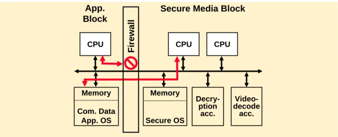
3) Hardware and software virtualization for strong hardware/software security
To achieve a secured system, the multicore hypervisor virtualizes hardware resources and an OS (Operating System) and applications are prohibited from accessing hardware resources directly. To isolate the secure media block and the application block effectively, we set up a firewall between the secure and the application blocks using software (Figure 6).
Decry- ption
acc.
CPU
Video- decode
acc.
Memory
Secure OS Memory
Com. Data App. OS
CPU CPU
Secure Media Block App.
Block
F ir e wa ll
Figure 6. Protection by software.
学位論文審査報告書(甲)
(外国語の場合は和訳を付けること。)
1. 学位論文題目
L.9.
史P.Q宵巳U?!.9.9.Y.
毘Qf.,n-_c;bj_t�
_c;W民旦JJ:ct.rrrnlt_i_c;_9.民-�P.P.r.Q.�.Gb.f.9x.巳mJ?竺gg
_�Q.. �Y.話巳坦F・一一一一一一一一一一一一一
ー
(組込み用ー途!育H :t :低消費電力_7_
_ロ土..'Y..:り:
__. __ _7_三主 £2.£ 土
ーと之/1(.£ヨヱ研芳)_
2. 論文提出者 (1)所 属 電子情報科学専攻
ふり がな おおたに す が
(2)氏 名 大谷 寿賀子 3. 審査結果の要旨(600~650字)
-
----�成
-�1.空..7 . .tl...�.$ ..日
.に第.J周空位前 .X.筈套 委員会.乏開催 L た?…閉
.日巳日頭発表玄実施-�-�--そ の後に第-�-聞き位論文寮査委員会乏閉催んた旦・ .t真草.審 議.<9.結果
1一以:f.V.通
ーロ判定-し-た旦ーなおし
ー口 頭発表
ーにおけ.9質疑去最終試験に賛A2.わ .V.. とLた-�-------··--·-··
___ JR'.r江lJt.
ぽP.-_句t9.f_ '.rhiP.-g号)が急速区普及ー L 始 j め-主--会主役機器が主立J
_'.才三三:交繋がる開 .1 古が到来
ー