T.G.Tsuru (tsuru@cr.scphys.kyoto-u.ac.jp)
20130506_Krakow_XRPIX_v5.key
S.G. Ryu, S.Nakashima, Matsumura, T.Tanaka (Kyoto), A.Takeda, Y.Arai (KEK), + SOIPIX group T. Imamura, A. Iwata, T. Ohmoto, T. Maeda (A-R-Tec) for Chip Design
M. Bautz, G.Y.Prigozhin, S.E.Kissel, B.LaMarr, R.F.Foster (MIT) for experiment of XRPIX1b-CZ-FI/BI
H. Nakajima, H. Tsunemi (Osaka) J.P.Doty (Noqsi) for design of ADC
Development of Kyoto’s X-ray Astronomical SOI pixel sensor
Ryu et al. IEEE NSS 2010, Conf. Record XRPIX1-CZ -FI Ryu et al. IEEE TNS 58, 2528 (2011) XRPIX1-CZ-FI
Tsuru et al. IEEE NSS 2011 Review
Ryu et al. IEEE NSS 2011, Conf. Record Event-Driven Readout system Nakashima et al. IEEE NSS 2011, Conf. Record XRPIX-ADC1
Nakashima et al. Physics Procedia 37, 1373 (2012) XRPIX1-FZ-FI
Ryu et al. IEEE TNS 60, 465 (2013) XRPIX1b-CZ-FI, Inter-pixel cross-talk
Takeda et al. IEEE TNS 60, 586 (2013) Event-Driven Readout with XRPIX1b-CZ-FI
Tsuru et al. SPIE Astro2012 Review
Nakashima et al. NIM A, Accepted (2013) XRPIX2
1
Publication
•
X-ray Astronomy•
“XRPIX”Kyoto’s X-ray Astronomical SOI pixel sensor
•
Depletion Layer and Dark current•
FZ of 2010 and 2012•
Spectral Performance•
Back Illumination•
Coming SoonTalk Plan 2
Optical Image
X線国際天文衛星 NeXT
1)はじめての硬X線の撮像観測を基に、
ブラックホール天文学に新展開をもたらす。
2)銀河団の質量の正確な決定をはじめて可能 とし、それを通じて宇宙の大規模構造の進化を 探る
銀河団は銀河の質量の数倍の質量を持つ高温ガスで満たされている。このガ ス分布はX線でのみ観測できる。ガスの温度(~億度)と広がりからダークマ ターの質量がわかり、銀河団の質量が決定される。
X線やガンマ線はブラックホールの極近傍(シュバルツシルト半径の数倍)か ら放出される(光や電波は遥かに外側)
4
X線による観測
可視光画像 X線画像
100個もの銀河が集団をなし、
宇宙で最大規模の構造を形成 しているのが見える
一千万度から一億度もの高温 ガスが重力の井戸に閉じ込め られているのが見える
X線は高温・高エネルギーの宇宙の姿を描き出す 宇宙に出る事で初めて観測が可能に。。
直接検出可能な物質の90%はX線のみで観測可能
X-ray Image Optical ImageX-ray Image
Cluster of Galaxies
Why X-ray Astronomy ? 3
~106 ly
The Andromeda Galaxy
• Hot plasma = several x sum of galaxies.
• Most of normal (baryonic) matter in the universe is visible ONLY in X-ray.
• Stars likes the sun in the optical.
• Blackholes and neutron stars in X-ray.
X-ray astronomy makes the hot and violent universe visible.
ASTRO-H (2015)
“The” standard Imaging Spectrometer
X-ray CCD Chandra (1999)
XMM-Newton (2000)
Suzaku (2005)
4
The standard Imaging Spectrometer of
modern X-ray astronomical satellites X-ray CCD
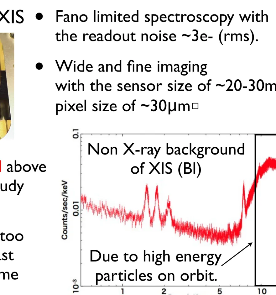
• Fano limited spectroscopy with the readout noise ~3e- (rms).
• Wide and fine imaging
with the sensor size of ~20-30mm pixel size of ~30μm□
Non X-ray background of XIS (BI)
Due to high energy particles on orbit.
•Non X-ray background above 10keV is too high to study
faint sources.
•The time resolution is too poor (~sec) to make fast timing obervation of time variable sources.
S26 K. Koyama et al. [Vol. 59,
2.4. Heat Sink and Thermo-Electric Cooler (TEC)
A three-stage thermo-electric cooler (TEC) is used to cool the CCD to the nominal operating temperature of −90◦C. The cold-end of the TEC is directly connected to the substrate of the CCD, which is mechanically supported by 3 Torlon (polyamide-imide plastic) posts attached to the heat sink. The heat is transferred through a heat pipe to a radiator panel on the satellite surface, and is radiated away to space. The radiator and the heat pipe are designed to cool the base below −40◦C under the nominal TEC operating conditions. Figure 5 is a photograph of the inside of base with the frame-store cover shield removed. Since the TEC is placed under the CCD, and the heat pipe is running under the base plate, these are not seen in figure 5.
2.5. Radiation Shield
The performance of any CCD gradually degrades due to radiation damage in orbit. For satellites in low-Earth orbit like Suzaku, most of the damage is due to large fluxes of charged particles in the South Atlantic Anomaly (SAA). The radia- tion damage increases the dark current and the charge transfer inefficiency (CTI). The XIS sensor body provides radiation shielding around the CCD. We found from the ASCA SIS experiment that radiation shielding of > 10 g cm−2 equivalent Al thickness is required. The proton flux density at 2 MeV on the CCD chip through 10gcm−2 of shielding is estimated to be
∼ 2×10³ protonscm−2MeV−1d−1 in the Suzaku orbit (same as the ASCA orbit) at solar minimum.
3. On-Board Data Processing 3.1. XIS Electronics
The XIS control and processing electronics consist of AE/TCE (analog electronics/TEC control electronics) and DE (digital electronics). The DE is further divided into PPU (pixel processing unit) and MPU (main processing unit). Two sets of AE/TCE are installed in each of two boxes, respectively, called AE/TCE01 and AE/TCE23. Similarly, 4 PPUs are housed in pairs, and are designated PPU01 and PPU23, respectively.
AE/TCE01 and PPU01 jointly take care of XIS 0 and XIS 1, while AE/TCE23 and PPU23 are for XIS 2 and XIS 3. One unit of MPU is connected to all the AE/TCEs and PPUs.
The AE/TCE provides the CCD clock signals, controls the CCD temperature, and processes the video signals from the CCD to create the digital data. The clock signals are generated in the AE with a step of 1/48 pixel cycle (∼ 0.5µs) according a micro-code program, which is uploaded from the ground.
The pixel rate is fixed at 24.4µs pixel−1. Therefore one line, consisting of 4 under-clocked pixels, 256 active pixels, and 16 over-clocked pixels, is read out in about 6.7 ms. The CCD output is sampled with 16-bit precision, but only 12 bits are sent to the PPU. The 12 bits are selected to cover the full energy scale of $ 15 keV in the normal setting of the gain. The full energy scale of $ 60 keV can also be selected in the low gain mode.
The AE/TCE controls the TEC (thermo-electric cooler) to generate a temperature difference of ∼ 50◦C relative to the base, while keeping the CCD chip at −90◦C. The AE/TCE
Fig. 5. The CCD and heat sink assembly installed in the base. The cover shield is removed in this picture.
can also supply reverse current to the TEC, to warm up the CCD chip in orbit. The CCD temperature may be raised a few tens of◦C above that of the base. In practice, the requirement to avoid excessive mechanical stresses due to differential thermal expansion of the copper heat sink relative to the alumina CCD substrate imposes an upper limit on CCD temperature in this mode. For example, with the heat sink at a typical operating temperature of −35◦C, we have adopted a maximum allow- able CCD temperature of about + 15◦C. The CCD temperature upper limit is higher at higher heat sink temperatures.
The PPU extracts a charge pattern characteristic of X-rays, called an event, after applying various corrections to the digital data supplied by the AE/TCE. Extracted event data are sent to the MPU. Details of the event extraction process are described in subsection 3.3. The PPU first stores the data from its AE/TCE in a memory called the pixel RAM. In this process, copied and dummy pixels1 are inserted in order to avoid a gap in the event data at segment boundaries, to ensure proper event extraction at segment boundaries and to enable identical processing of all segments of the data. The raw data from AE/TCE may include a pulse height (PH) offset from the true zero level due to dark current, small light leakage through the OBF, and/or an electric offset. Since the offsets depend on the CCD position and time, offset corrections are also position and time dependent. To reduce the computing power and time required for such corrections, the offsets are divided into two parts, dark-level and light-leak. The dark-level is the average output from a pixel with no irradiation of X-rays or charged particles. The dark-level is determined for individual pixels, and is up-dated by command only after each SAA passage in
1 The data of each CCD segment are transferred through independent lines from the AE/TCE to the PPU, and are processed in parallel by the same processing scheme in the PPU. For a proper event extraction at the segment boundary, the data in the two columns of the adjacent CCD segments must be used. Therefore hard-wired logic is installed to “copy”
the two column data in the adjacent CCD segments to the proper locations in the PPU pixel RAM. These are called as “copied pixels”. In the case of outer boundaries of segments A and D, such “copied pixels” can not be prepared. Instead, two columns of zero data are prepared in the PPU pixel RAM. These are called “dummy pixels” in the PPU pixel RAM.
Suzaku「すざく」 XIS
5
“XRPIX” = Monolithic SOI pixel sensor for future X-ray astronomical satellites
10μsec
Target Spec.
Imaging area > 25x25mm2, pixel ~ 30-60μm□ (1” @ F=9m)
Energy Band 0.3-40keV with BI (<0.1μm), and thick depletion (>250μm) Spectroscopy ΔE < 140eV @ 6keV, Fano limit (Req.<10e-, Goal < 3e-)
Timing <1μsec
Dark Current <2pA/cm2 (assuming working T = -40℃)
Function Trigger signal & pixel address output, built-in ADC Non X-ray BGD 5e-5 c/s/keV/10x10mm2 at 20keV (1/100 of CCD)
Very low BGD by anti-coincidence (1/100 of CCD at 20keV)
on-board processor
non X-ray (high energy BGD
particle)
X-ray
scintillator
Each pixel has its own trigger and analogue readout CMOS circuit.
Fast CMOS (low ρ Si)
Insulator (SiO2)
V_back
Hole Electron
V_sig Time
X-ray
BPW
ReadoutCMOS ReadoutCMOS
ReadoutCMOS
P+
ReadoutCMOS
Sensor (high ρ, depleted Si)
Our SOIPIX (XRPIX)
6
XRPIX Series - Road Map -
2010 2011 2012 2013
XRPIX2
XRPIX1 XRPIX1b
A-R-Tec PROPRIETARY/CONFIDENTIAL 2.4mm 5 2.4mm
XRPIX ΔΣ-type
ADC 2.4 mm 2.4 mm
2.4 mm
6.0 mm
1.0 mm
1.0 mm 4.0 mm
X-ray imaging area
XRPIX2b
4.5 mm
6.0 mm
7
XRPIX1-CZ (0.7kΩcm), -FZ(2010) (7kΩcm): Depletion Depth
Back Bias [V]
0 10 20 30 40 50
Depletion Depth [um]
0 50 100 150 200 250 300 350
60 70 80 90 100 110
Back Bias [V]
0 10 20 30 40 50
Depletion Depth [um]
0 50 100 150 200 250 300 350
60 70 80 90 100 110
FZ : 250μm @ VBB=30V
• Measure the depletion thickness by observing the ratio between the counting rates of two energies X-rays having different attenuation
lengths.
• CZ: Depletion thickness of 150μm at VBB=100V.
• FZ: Full depletion of 250μm is achieved at VBB=30V.
CZ : 150μm @ VBB=100V
+ : Experimental results – : Expected value
Nakashima et al., 2012, Physics Procedia 37, 1373
8
FZ : Physical Thickness
XRPIX1b-FZ(2012)-FI (7kΩcm) : Depletion Depth
back_bias 200V
• Counting Rate of 22keV X-ray (Cd-109) as a function of VBB.
(Attenuation Length = 1200μm > Physical Thickness = 500μm.)
• The data follow the expected slope of depletion VBB^1/2.
• Full Depletion is reached at VBB=200V.
20130502_matsumura.pdf
Depletion VBB^1/2
9
Preliminary
Physical Thickness 500μm (not 260μm)
Counting Rate of 22keV X-ray
Confidential
© 2011 LAPIS Semiconductor Miyagi Co., Ltd. All Rights Reserved
FWP-300377
a) MX1542-001JA (HR1) b) MX1542-002JA (N FZ)
Confidential
© 2011 LAPIS Semiconductor Miyagi Co., Ltd. All Rights Reserved
FWP-300377
CV 2mm x 1mm HR1 1.7k cm
2k cm N FZ 6.6k cm
HR1 / N FZ Ave. 40%
300um
N FZ HR1 6.3k cm
HR1 2
a) b) c)
XRPIX1b-FZ(2012)-FI (7kΩcm) : Depletion Depth
• 500μm @ VBB=200V
→ ρ=4kΩcm < average (7kΩcm)
• ρ is different from position to position on a wafer.
• Check which wafer used in this device.
121001_MX1542_Lapis.pdf
10
From 20110516_OKImeeting_SOI_Dark_v5
XRPIX1/1b-FZ(2010/12)-FI (7kΩcm) : Dark (Leak) Current
• XRPIX1-FZ(2010)
• Wafer Thickness 260μm
X線CCDの暗電流は約3桁低い
Temperature (degree C) -50 -40 -30 -20 -10 0 10 20
Dark Current (e/ms/pixel)
10-3
10-2
10-1
1 10 102
103
104
105
106
Black:VBB=30V Blue :20V
Red :10V
Dark Current (e/msec/30.6μm□ pixel)
FZ (2010)
Consists of two components.
(1) Depend on T and VBB.
generation in depletion layer.
(2) Almost Constant.
10e/msec = 1.6fA Next Slide
FZ (2012) VBB=20V
3e-2
4e-3 PchNeXT4
• XRPIX1b-FZ(2012)
• Dark is 1/10 of FZ(2010) (at the same VBB)
expectation FZ (2012)
VBB=30V
11
1/10
Eliminating the constant component reach the target specification.
Target Spec. at -40C (depletion 250μm) = 0.1e/1msec/30.6μm□ =2pA/cm2
(N_SENS) PMOS(P13)
Leak Current from Protection Diode (Arai-sensei)
• Simulation shows leak current from PMOS used as a protection diode at the sensor node is 2fA = 12.5e/msec.
• Possibly explains the constant component.
• Gate length of the PMOS = 0.2μm → 1μm.
Reduce leak current 2fA → 0.02fA.
12
Protection diode
Sensor node
Source Follower
XRPIX2-CZ-FI (Small Pixel) : Spectrum
Nakashima et al., 2012, NIM A submitted
0 2 4 6 8 10 12 14 16 18 20
0 20 40 60 80 100 120 140
0 10 20
0 150
50 100
X-ray Energy (keV)
Pulse Hight (ch)
XRPIX2 Gain 6.5 µV/e-
XRPIX1 Gain 3.6 µV/e-
Observed Readout
Noise Fano
Noise Pixel-Pixel Gain
Dispersion 1% Sum Cu Kα 656 eV 548 eV (FWHM)
64 e-(rms)
139 eV 255 eV 620 eV
Mo Kα 800 eV
548 eV (FWHM)
64 e-(rms) 205 eV 553 eV 805 eV
PH [ADU]
40 60 80 100 120 140 160
PH [ADU]
40 60 80 100 120 140 160
0 200 400 600 800 1000 1200 1400 1600 1800
40 80 120 160
Pulse Hight (ch = 244 µV) 1000
500 1500
Cu Count
100 200
0 0
Mo Count
Cu Kα (8.0 keV) Mo Kα (17.4 keV)
Mo Kβ (19.6 keV) 656 eV
FWHM
800 eV FWHM
Readout Noise 100→64e-
13
Charge Amp Feedback
Capacitance Sensor
Node
Reset SW
Coming Soon 1 / Pre Amp in Each Pixel 14
• A charge sensitive amp in every pixel in order to increase the gain.
• This is basically the same amp used in PIXOR.
• Gain ~100 μV/e, higher by a factor of ~15.
• Readout noise = 64e (rms) → ~4e (rms).
XRPIX3
Protection Diode
XRPIX1b-CZ : Single Pixel Readout
• In order to study the soft X-ray performance.
• Observe the waveform of analogue output from a single pixel by fixing the readout address without clocking (Single Pixel Readout like a SSD).
• Detect an X-ray as a “step” and measure the pulse height. → X-ray spectrum.
• No reset during the measurement → Free from the reset noise
• Reduce noises other than the reset noise by introducing LPF.
high_v(100 samples average) - low_v(100 samples average) → LPF with τ=100μs
sample number in one frame
0 200 400 600 800 1000
PH [ADU]
625 630 635 640 645 650 655 660
sample number in one frame
0 200 400 600 800 1000
PH [ADU]
627 628 629 630 631 632 633
PH [ADU]
0 50 100 150 200
Cts / ADU
1 10 102
103
104
CMS Histgram h1
Entries 49668 Mean 0.2479 RMS 1.017
CMS Histgram
Data Name: Fe_minus30c_sp_Vback_100V_Tscan_480ns_25_25_50000f.root
Cut+Ped+Phy[frm]: 300+500+50000
Hit threhold= 10 ADU, Delay=2 frm, Ave=160 frm X-ray count: 0.001972 Cts/frame
Readout Noise = 0.330654 ADU
X-ray Hit
Pulse Height
average
100 samples τ=100μsec
h1
Entries 398490
Mean 0.3396
RMS 3.101
/ ndf
χ2 3.97e+05 / 9
Constant 85.81 ± 1.41 Mean 54.28 ± 1.41 Sigma 0.8022 ± 11.6984
PH [ADU]
0 20 40 60 80 100 120 140
Cts / ADU
0 20 40 60 80 100 120
h1
Entries 398490
Mean 0.3396
RMS 3.101
/ ndf
χ2 3.97e+05 / 9
Constant 85.81 ± 1.41 Mean 54.28 ± 1.41 Sigma 0.8022 ± 11.6984
CMS Histgra (R10C10)
FWHM=278eV @8.0 keV
rms=14.6e- 44M-BPW
Cu-Kβ Cu-Kα
ΔE = 278eV @ 8.0keV (FWHM), readout noise = 14.6e (rms) average
100 samples τ=100μsec
Nakashima et al., 2012, Physics Procedia 37, 1373 Ryu et all, 2013, IEEE TNS 60, 465
15
XRPIX1b-CZ-FI/BI (100μm): Spectra in Single Pixel Readout (2011.11.22)
Target= Al2O3 , Front-I, Back-I, V_tube=6 kV,
V_bais = 100V, Temp=–50ºC, Hit Threshold= 2 ADU, Exposure=400 sec, PIX=R10C10, 2us_sample, 300 µs_ave
h4
Entries 128627 Mean 1.608 RMS 3.417
PH [ADU]
-5 0 5 10 15 20 25 30 35 40
Cts
1 10 102
103
104 h4
Entries 128627 Mean 1.608 RMS 3.417
CMS Histgram (offset-corrected)
h4
Entries 128627 Mean 1.608 RMS 3.417
AL-Ka (1.48 keV)
Si Edge (1.84 keV)
RED: BI BLUE: FIEntries h4 128627
Mean 2.282
RMS 3.155
PH [ADU]
0 1 2 3 4 5 6 7 8 9 10 11 12 13 14
Cts
0 100 200 300 400 500 600 700 800 900 1000 1100 1200
h4
Entries 128627
Mean 2.282
RMS 3.155
CMS Histgram (offset-corrected)
h4
Entries 128627
Mean 2.282
RMS 3.155
Zoom
O-Ka ??
(6kV)HV
←15 e-rms
←18 e-rms
Cts
Detection Threshold
(2ADU)
502 eV
by Calibration
AL-Ka
• Back illumination type.
• X-ray generator (target = Al, 6kV).
• Al-K + Bremss
(+O-K from Al2O3?)
• ΔE (FI) = 188eV,
ΔE (BI) = 351eV (if line)
• Absolute and relative X-ray Fluxes are uncalibrated.
→ QE and dead layer thickness are unknown.
Results on FI : Ryu et al., IEEE TNS 60, 465 (2013)
16
QE of LBNL’s BI-SOIPIX / SOImager-2-CZ-BI
Deplation 73±2μm Dead Layer
0.6±0.2μm
Battaglia+12 NIM-A
Coming Soon 2 / “Pizza Process” 17
• The Pizza proc. is now being made at LBNL.
• Evaluation of low energy X-ray spectral performance.
Pizza Process to FZ devices of XRPIX
• Pizza Proc. is the back side process developed by LBNL.
• CZ-BI with Back- thinned to 70μm.
• A thin phosphor layer is implanted.
• Dead Layer : 0.6±0.2μm
Summary
SOI Pixel Project : General View
Feb. 28, 2011
SOI International Review Meeting Yasuo Arai, KEK yasuo.arai@kek.jp
http://rd.kek.jp/project/soi/
/TEG
URL: http://www.a-r-tec.jp Email: info@a-r-tec.jp
A-R-Tec
Analog and RF Technologies
• We have been developing monolithic SOI sensor ‘XRPIX’
for future X-ray Astronomical Satellites.
• It contains the function of trigger signal output for the
anti-coincidence, which realizes very low non-X-ray BGD.
• We successfully developed the test devices with the depletion thickness of ~250μm.
• Under going
• Improvement of the readout noise.
• Reduction of dark current.
• Test with new back side process (Pizza Proc.).
18