Japan Advanced Institute of Science and Technology
JAIST Repository
https://dspace.jaist.ac.jp/
Title ドーピングによりグラフェンナノリボン内化学ポテン
シャルを空間的に制御した量子ドット形成の研究
Author(s) Wang, Zhongwang Citation
Issue Date 2020‑03‑25
Type Thesis or Dissertation Text version ETD
URL http://hdl.handle.net/10119/16663 Rights
Description Supervisor:水田 博, 先端科学技術研究科, 博士
Spatial Chemical Potential Engineering for Quantum Dot Formation in Graphene Nanoribbon via Controllable Doping
Intended degree: PhD Advanced Science and Technology Mizuta Laboratory 1720004 WANG Zhongwang
Research Content:
Graphene is of interests to fundamental physics studies as well as to novel applications in electronic devices owing to its many appealing properties such as very high carrier mobility, unique spin quantum Hall effect, high Young’s modulus, etc. It is known that by patterning graphene to a nanoribbon (GNR) with a width of a few tens of nanometer, an effective energy gap can be opened.[1] However, electrons in an etched graphene nanostructure are inevitably subjected to the disorders caused by localized charge states originated from the surrounding environments, e.g., substrate defects, surface adsorptions, organic residues and edge roughness.[2] Interestingly, carriers can tunnel through the isolated localized states enable quantized transport features. [3] By properly control the disorder and their effects, one could either erase the localization features or intentionally build a quantum dot (QD). Suspended graphene, on one hand, is free from substrate disorders, therefore it exhibits almost intrinsic properties. On the other hand, it is difficult to fabricate and fragile. For non-suspended graphene devices, one solution is applying a bias voltage to a local gate. Alternatively, one could introduce chemical doping to a graphene device. By developing a controllable doping method with nanometer scale spatial resolution, we could reconstruct the energy profile of a GNR to a structure similar to a single QD as the illustrated in Fig 1. In this work, we focus on the doping control to realize QD-like single electron transistor (SET) behavior in a solo GNR.
Hydrogen silsesquioxane (HSQ) is a negative tone e-beam resist with a resolution of ~ 20 nm. For GNR, HSQ can be used as etching mask as well as dopant source because HSQ can provide both hydrogen atoms (n-type doping) and oxygen atoms (p-type doping). Moreover, the spicy and amount of dopants to graphene depends on the e-beam irradiation dose. [5]
Thanks to the fine spatial resolution of e-beam lithography technology, we are able to precisely introduce doping to desired position of a GNR by using the dose-controlled e-beam irradiation doping method (see Fig 2). At low temperature (5 K), the expected single QD-like properties,
i.e., separate diamond patterns with clear edges, are observed in a doping controlled GNR with a width of 30 nm and a length of 60 nm as shown in Fig 3. The geometry design rule for single QD-like behaviour will be also discussed in the presentation. In addition, a method to fabricate suspended graphene double quantum dot with small deformation will also be introduced for the future prospect.
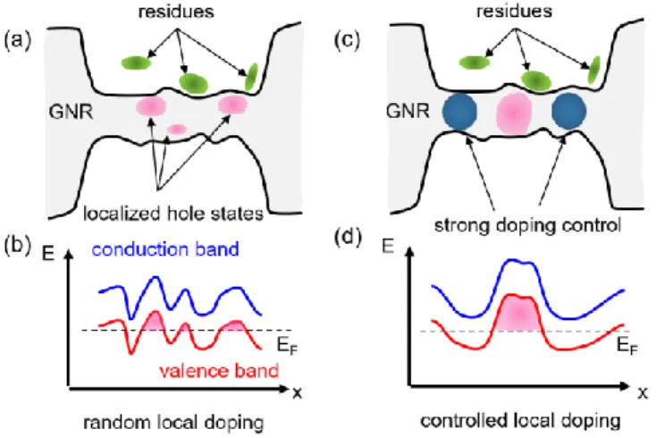
Figure 1. Illustration of the hole localization states and the corresponding energy profile in (a) , (b) non- treated and (c), (d) doping controlled graphene nanoribbons (GNRs). Without any doping treatment, the edge roughness and fabrication residues dominate the energy profile fluctuation (Fig 1 (c)), resulting in random localized hole states in GNR body (Fig 1 (a)). With precise doping control, one can intentionally dope the desired positions of GNR. For instance, on the ends of the GNR (Fig 1 (c)), then the energy profile can be reconstructed as illustrated in Fig 1 (d).
Figure 2. (a) Top profile is the schematic of the designed energy diagram of the controllably doped GNR for constructing a quantum dot. The chemical potential in the center of GNR is ΔED higher than that of the two ends connected to the leads. The middle profile is the geometric design of the HSQ capping layer with varied doses (top). The wide leads (gray) are exposed with a low dose of 900 μC/cm2, whereas the center of the short ribbon (red) is exposed with a high dose of 1800 μC/cm2. Two 8 nm long gaps (blue) inserted between the leads and the GNR are unexposed during lithography. The bottom is the scanning electron microscopic image of the fabricated device scale bar 100 nm. (b) Source-drain conductance (Gsd) verses back gate voltage transfer curves measured in the device with a 30 nm wide and 60 nm long GNR at room temperature and 5 K. Bias Vsd = 1 mV. At 5 K, a low conductance with oscillation peaks (so called transport gap) is read.
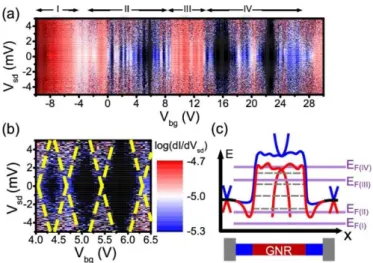
Figure 3. (a) Charge stability diagram measured in the GNR device with the width of 30 nm and length of 60 nm at 5 K. (b) Zoomed-in details of region II in (a) showing the single quantum dot like transport feature.
(c) Schematic energy band diagram of the device. Blue and red solid lines indicate the bottom of the conduction band and top of the valence bands, respectively. Fermi levels are marked corresponding to the four regions, I, II, III, and IV, marked in (a).
References
(1) M. Y. Han, B. Özyilmaz, Y. Zhang and P. Kim, Energy Band-Gap Engineering of Graphene Nanoribbons.
Phys. Rev. Lett. 98, 206805, (2007).
(2) D. Bischoff, A. Varlet, P. Simonet, M. Eich, H. C. Overweg, T. Ihn, and K. Ensslin, Localized Charge Carriers in Graphene Nanodevices. Appl. Phys. Rev. 2, 031301, (2015).
(3) C. Stampfer, J. Güttinger, S. Hellmüller, F. Molitor, K. Ensslin and T. Ihn, Energy Gaps in Etched Graphene Nanoribbons. Phys. Rev. Lett. 102, 056403, (2009).
(4) M. Eich, R. Pisoni, H. Overweg, A. Kurzmann, Y. Lee, P. Rickhaus, T. Ihn, K. Ensslin, F. Herman, M.
Sigrist, and K. Watanabe, Spin and Valley States in Gate-Defined Bilayer Graphene Quantum Dots. Phys.
Rev. X, 8, 031023, (2018).
(5) K. Brenner and R. Murali, Single Step, Complementary Doping of Graphene. Appl. Phys. Lett. 96, 063104 (2010).
Research Purpose:
Graphene based QD and SET are promise candidates for spin q-bit and ultra-high sensitive charge detector. However, the disorders such as edge roughness and random local doping caused potential profile fluctuation and the consequent multiple QD-like features heavily affect the device properties. It is also believed the disorders are the reason why the promising spin blockade has not been observed so far. To improve the device properties, scientists attend to reduce the impacts of disorders by etching away the SiO2 substrate, using h-BN instead of SiO2
as the substrate, advanced patterning technology, changing the QD design from a disc island to a solo GNR, etc. However, the disorders can not be completely removed by the current technology.
Instead of removing the disorders, we come up with a different concept of doping control.
Because in principle, the key to construct QD is a double barrier box to confine the electrons.
If we could precisely control over the local doping, we could construct the QD-like potential profile. Therefore, it is not necessary to remove the disorders. Following this concept, we preformed our experimental studies and investigations. The key experimental observation is shown in Fig 3. Not only the single-QD like diamond patterns in Region II, but also the overlapped diamond patterns without clear edges (signature of multiple QDs, typical transport characteristic in those GNRs without doping control) in Region IV, indicating the existence of potential fluctuation. Although, we see the single QD-like features in Region II is not affected by the disorders from the experimental results.
Our work on doping controlled GNR provides a new strategy to realize QD. In the future, a local top gate will be attached on the GNR center to tune the potential in the QD region. Also, the single QD GNR will be extended to double, triple QDs with several tuning top gates for the integration experiments.
Key words: graphene nanoribbon, disorder, doping control, single quantum dot, HSQ