SUMMARY We describe a field experiment of flexible modulation for- mat adaptation on a real-time 400 Gbit/s/ch DSP-LSI. This real-time DSP- LSI features OSNR estimation, practical simplified back propagation, and high gain soft-decision forward error correction. With these techniques, we have successfully demonstrated modulation format allocation and trans- mission of 56-channel 400 Gbit/s-2SC-PDM-16QAM and 200 Gbit/s-2SC- PDM-QPSK signals in 216 km and 3246 km standard single mode fiber, respectively.
key words: adaptive modulation, field trial, real-time DSP, 400 Gbit/s
1. Introduction
Applying a digital signal processing technique with coherent detection significantly increases the transmission capacity and reduces the cost of optical communication networks. In 2011, we reported on 80×100 Gbit/s/ch WDM transmission over 6×70 km of installed fiber using real-time digital signal processing circuits (DSPs) enabled by polarization division multiplexing (PDM) quadrature phase shift keying (QPSK), soft-decision low-density parity-check code of 10.8 dB net coding gain (NCG) and fast chromatic dispersion estimation [1]. The key functions of the real-time DSP, i.e. short time channel recovery of 12 msec, are realized by a fast chromatic dispersion estimation technique that works before demodu- lating the data signal.
To accommodate even higher data traffic increases, Manuscript received November 30, 2016.
Manuscript revised February 23, 2017.
Manuscript publicized April 20, 2017.
†The authors are with NTT Network Innovation Laboratories, NTT Corporation, Yokosuka-shi, 239-0847 Japan.
††The author is with NTT Access Network Service Systems Laboratories, Yokosuka-shi, 239-0847 Japan.
†††The authors are with NEC Corporation, Kawasaki-shi, 211- 8666 Japan.
††††The authors are with Fujitsu Limited, Kawasaki-shi, 211-8588 Japan.
†††††The authors are with Mitsubishi Electric Corporation, Kamakura-shi, 247-8501 Japan.
∗Presently, with NTT Electronics, Japan.
a) E-mail: [email protected] DOI: 10.1587/transcom.2017OBI0003
400 Gbit/s/ch transmission systems are being intensively studied[2]–[4]. Although only PDM-QPSK was supported in 100 Gbit/s/ch, multilevel modulation formats i.e. PDM- QPSK, PDM 8 quadrature amplitude modulation (QAM), and PDM-16QAM are in strong demand for 400 Gbit/s/ch.
This is because more choices of modulation format allows more suitable assignment in accordance with the various link condition, which leads the reduction of the excess margin and the CAPEX[5],[6]. To minimize such a margin, it is neces- sary to grasp the fiber conditions accurately. One metric, the optical signal to noise ratio (OSNR), is widely used because of its accuracy. By measuring the OSNR, we can estimate the signal quality against amplified spontaneous emission (ASE), which is the main degradation effect in transmission.
Hence, we have proposed and demonstrated a pilot-aided OSNR estimation scheme for modulation format adaptation with offline signal processing[7]–[9].
This paper introduces the real-time experiment with modulation format adaptation based on pilot-aided OSNR estimation. We used a real-time DSP and field-installed standard single mode fiber (SSMF). The real-time DSP has several key techniques for 400 Gbit/s adaptive modu- lation: OSNR estimation, practical simplified back propaga- tion method, and high gain soft-decision forward error cor- rection (FEC). By adapting the modulation format to suit the estimated OSNR, 56-channel 400 Gbit/s 2-Subcarrier (SC) PDM 16QAM and 200 Gbit/s 2SC-PDM-QPSK signals are successfully transmitted over 216 km of field-installed SSMF and 3246 km of SSMF (216 km field fiber + 3030 km labora- tory fiber). Long-term stability in Q-factor is also confirmed for both modulation formats. Adding to the previous pa- per[10], we present a detail configuration and highlighted techniques of the 400 Gbit/s real-time DSP.
This paper is organized as follows. In Sect. 2, the signal processing flow and key techniques of the real-time DSP- LSI are presented. The transmission results for adaptive modulation format allocation and long-term measurement of 56-channel 400 Gbit/s-2SC-PDM-16QAM and 200 Gbit/s- 2SC-PDM-QPSK are shown in Sect. 3. Section 4 draws our conclusion.
Copyright © 2017 The Institute of Electronics, Information and Communication Engineers
Fig. 1 Configuration of real time DSP based optical transponder.
2. Real Time DSP-LSI for 400 Gbit/s/ch Transport
2.1 Block Diagram of Real-Time DSP-LSI
Figure 1 shows an overview of the real-time DSP based optical transponder. This transponder consists of a digital coherent optical transmitter and receiver parts. At the trans- mitter, client signal (one or two 100 GbE) is fed to a framer that converts the client signal format from Ethernet to Opti- cal Transport Network (OTN). The signal then proceeds to the DSP-LSI part (the gray area in Fig. 1). At first in the DSP, parity bits for FEC are added to the OTN signal. The maximum redundancy for soft decision and hard decision FEC is 25.5%. The coded signal is mapped to 4-lane QPSK or 16QAM according to the number of input client signals.
After that, two kinds of pilot signals for transmission path estimation are inserted into the signal. These pilot signals are utilized to estimate the various types of transmission path distortion; one can estimate the frame timing, chromatic dis- persion, frequency offset, and OSNR, the other can estimate the phase noise. To pack the 100 Gbit/s-QPSK or 200 Gbit/s- 16QAM signals into the 37.5 GHz grid for improved spectral efficiency, data and pilot signals are spectrally shaped by a Nyquist filter at an arbitrary roll off factor in a spectral shap- ing function block. In addition, the transfer function of the hardware and the skew at the transmitter are compensated in the same block. Following the digital analog converter (DAC), the signal moves on to the optical transmission part constructed of laser source, optical modulator, driver ampli- fier, and auto bias control. Then the signal is launched to the optical fiber transmission link. The modulation format is 100 Git/s-PDM-QPSK or 200 Gbit/s-PDM-16QAM. At the digital coherent optical receiver, the transmitted OTN signal is received by the optical reception part composed of local oscillator, 90◦ optical hybrid, balanced photodetector, and transimpedance amplifier. The received signal is input to the DSP part and converted into a digital signal by an analog digital converter (ADC). At the entrance of the DSP-LSI, the signal is split into two paths; transmission distortion es-
timation path and main signal demodulation path. In the former, distortions generated in the optical fiber link such as chromatic dispersion, frequency offset, and OSNR degrada- tion are estimated by utilizing the pilot signal, moreover the timing of the pilot signal corresponds to frame location can be detected. The obtained parameters is fed to the functions on the main signal demodulation path. In the latter path, spectrum shaping and skew compensation for reception part are applied to the signal. After that, linear distortion; i.e.
chromatic dispersion and frequency offset are compensated using the parameters estimated by the transmission path es- timation block. Additionally, nonlinear distortion, which depends on signal intensity of self channel; i.e. self-phase modulation (SPM), is compensated by the low-complexity simplified back propagation method. Polarization alignment and residual linear distortion compensation are realized by a 2×2 multi input multi output (MIMO) adaptive equalizer (AEQ) with constant modulus algorithm (CMA) for QPSK and radius directed equalizer (RDE) algorithm for 16QAM.
To realize low latency and stable operation, the pilot sig- nal is used for initial convergence in AEQ. The signal then proceeds to the carrier phase recovery block, which compen- sates the signal phase by the Viterbi & Viterbi phase esti- mation (VVPE) method for QPSK, whereas modified VVPE is utilized for 16QAM. The equalized signal is converted from complex expression to binary expression by the signal demapper. The binary sequence is then corrected with soft and hard decision concatenated FEC. Finally, an Ethernet signal whose rate is comparable to that of the transmitter;
i.e. one or two 100 GbE, is obtained from the de-framer. It should be noted that we select QPSK or 16QAM for a modu- lation format candidate in this paper; however, this real-time DSP-LSI can treat 8QAM for an intermediate transmission condition between QPSK and 16QAM[11].
2.2 Key Techniques of Real-Time DSP-LSI
In this section, we introduce the key techniques of the real- time DSP-LSI: OSNR estimation, simplified digital back propagation (DBP), and high gain FEC.
in both X and Y polarization. Since the PS is a BPSK mod- ulated sequence, the spectrum has two peak components as shown in Fig. 2(b). The feature of this estimation is that we can measure in-band noise that shares the same frequency as the data spectrum at the PS position. Out-of-band OSNR estimation that measures the power at frequency adjoining the signal spectrum as the noise power can be utilized with- out PS; however the estimation accuracy deteriorates when the noise spectrum suffers. For example, the noise power is estimated higher than expected when the guard interval of the WDM signals is narrow because it is difficult to divide the noise spectrum from the signal spectrum; and the noise power is estimated lower than expected when the noise spec- trum are cut by band pass filter located before the reception.
The in-band OSNR estimation process begins with frame synchronization to detect the PS location following A/D conversion and resampling. We can find the PS posi- tion by searching for the biggest power timing in a received sequence adapted band pass filter, which extracts two peak components. It is because the whole spectrum components of the PS are covered by the band pass filter whereas most frequency components in the data sequence are lost. Af- ter detecting the PS, we compensate the frequency offset and chromatic dispersion using PS. Then, we calculated the noise power from the power spectral density between the two peak components. We ignore the frequencies close to direct cur- rent, because they sometimes contain the unwanted leakage of carrier component due to bias control imperfection in the IQ modulator caused by environmental thermal fluctuation.
Last, we derive the estimated OSNR by taking the ratio of the noise power and the signal power calculated using the data sequence.
In the multi-level modulation format for beyond 400 Gbit/s/ch; e.g. 8 QAM or 16QAM, fiber nonlinearity is one of the major problems. Although various nonlinear mitigation techniques have been proposed, DBP is highly attractive as it does not need additional dedicated optical devices and can be processed in the DSP. However, its com- putation complexity is significant since DBP uses a lot of cas- caded fast Fourier transform (FFT) and inverse fast Fourier transform (IFFT) operations to compensate the interaction between nonlinear effects and linear effects; i.e. Kerr effects and chromatic dispersion. To reduce DBP complexity, we
ular LDPC code[14]. To achieve good performance, care- ful combination is necessary. A parity-check matrix of a spatially-coupled LDPC code has a structure in which mul- tiple sub-matrices are placed at an angle. Since non-zero elements in the matrix are locally dense, the structure can contain many short cycles that cause an error-floor at a high BER, especially in the case of irregular LDPC codes. The proposed method reduces the occurrence of such short cy- cles by permuting a subset of rows in the parity-check matrix.
This lowers the error-floor and suppresses residual error bits.
Thus, a weak BCH code (with low redundancy) is able to eliminate the error-floor, and more parity bits can be allo- cated to the LDPC code.
To fit the LDPC codes in the optical channel transport unit – level k (OTUk) frame, which is standard in optical transport network, we set the code length to 38400 bits and parity bits to 7568. Therefore, this LDPC (38400, 30832) code has 24.5% overhead. When concatenated with BCH (30832, 30592) with a redundancy of 0.78%, which corrects 16-bit errors, the total FEC redundancy is 25.5%.
The error correction performance of the proposed FEC was evaluated by Monte Carlo simulation in an additive white Gaussian noise (AWGN) channel with various modulation formats, such as QPSK, 8QAM and 16QAM. We used a simplified δ-min LDPC decoder with 4 soft-decision bits.
Fig. 3 shows the simulation and experimental results. It was confirmed that high error-correction performance was yielded in the 100 Gbit/s real-time trials. The net coding gain is around 12.0 dB at the post-FEC BER of 10−15. 3. 400 Gbit/s/ch WDM Field Experiment
3.1 Experimental Setup
Figure 4 provides a schematic of the setup used in the field demonstration of modulation format adaptation via the real- time DSP [10]. We constructed a network model con- sisting of three photonic nodes (Node #1–3) with a 1x9 wavelength selective switch (WSS) and two fiber transmis- sion lines: 216 km field-installed standard single mode fiber (SSMF), 3030 km laboratory SSMF linking Node #1 to #2, and Node #2 to #3, respectively. As the main channels, we used two real-time DSP based optical transponders for
Fig. 3 Simulation and experimental results of the error correction perfor- mance of the proposed FEC.
Fig. 4 Experimental setup.
generating super-channel signals, i.e. 400 Gbit/s-2SC-PDM- 16QAM and 200 Gbit/s-2SC-PDM-QPSK signals. The transmitter and the local oscillator of the transponders had laser linewidth of 100 kHz. We used a Nyquist filter with roll off factor of 0.1. As background channels, we used 112 wavelength laser sources with laser linewidth of 100 kHz.
Fifty-six even and odd optical carriers with 75 GHz spacing in the C-band were independently modulated by separate IQ- modulators and polarization-multiplexed signals were gener- ated by a self-delayed polarization multiplexer (Pol.-MUX).
The even and odd wavelength division multiplexed (WDM) signals were optically multiplexed by Node #1 generating a 37.5 GHz-spaced background WDM signal. In Node #1, two wavelengths of the background WDM signal were replaced by two channels from two real-time DSP-based transponders.
The total capacity per fiber reached 11.2 Tbit/s with PDM- QPSK, and 22.4 Tbit/s with PDM-16QAM. The resulting WDM signal, including two real-time wavelengths, was fed into the first transmission line, i.e. 216 km field-installed SSMF. They were further transmitted to the second trans- mission line, i.e. 3030 km laboratory SSMF. The transmitted signal was dropped in Node #2 after 216 km transmission or
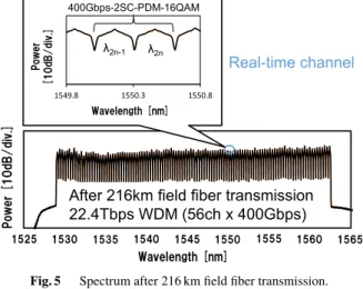
Fig. 5 Spectrum after 216 km field fiber transmission.
Fig. 6 Configuration of JGN-X field fiber.
Node #3 after 3246 km transmission in accordance with the experimental scenario. At the receiver, we selectively re- ceived one of the signals dropped in Node #2 or Node #3.
Finally, the two channels forming the super-channel were simultaneously received and demodulated by two real-time DSP-based optical transponders. We used a control PC for monitoring the DSP outputs: bit error rates (BERs) before FEC decoding (pre-FEC BER), after FEC decoding (post- FEC BER), estimated OSNR and constellation mapping. In addition, instructions for modulation and demodulation for- mat were fed to the DSP via the control PC.
Figure 5 depicts the spectrum after 216 km field fiber transmission. The WDM channels ranged in the full C-band from 1529.114 nm to 1562.283 nm. The two channels from the real-time DSP were set at 1550.15 nm and 1550.45 nm as channels 72 and 73, respectively.
The field SSMF is a part of the JGN-X testbed fiber cable installed between NICT Koganei Headquarters and TOKAI Chofu Repeater Station, Tokyo. Figure 6 shows the configuration of the JGN-X field fiber. The cable length is 18 km including 10 km aerial section. Twelve fiber cores were used for the 216 km transmission line, with 120 km aerial section. A gain equalizer (GEQ) was inserted mid span of the 216 km field fiber to flatten the power spec- trum. Considering the transmission loss of the field fiber (around 0.278 dB/km) and GEQ loss, we set the span length
to the transmission link condition by using the estimated OSNR as the criterion. PDM-16QAM was selected when the estimated OSNR was higher than OSNR threshold (20 dB in this experiment), otherwise PDM-QPSK was selected.
The detailed selection process is described in [9]. After deciding the modulation format, we measured the pre-FEC BER, post-FEC BER upon changing the channel number of the two real-time optical transponders from 1 to 56. We simultaneously received and processed the super-channels by real-time DSP-based transponders. Second, we switched the WSS in Node #2 from drop to through mode, then measured the estimated OSNR at Node #3 and set the appropriate modulation format for 3246 km transmission. We measured pre-FEC and post-FEC BERs for all channels in the same manner as with 216 km transmission.
Figures 7 and 8 depict the measured Pre-FEC Q-factors, estimated OSNR and constellation after 216 km and 3246 km transmission. In Fig. 7, estimated OSNRs were higher than the OSNR threshold, 20 dB, for all channels; thus, we could see PDM-16QAM was appropriate modulation format in 216 km transmission. Measured pre-FEC Q-factors were approximately 6 dB for all channels and we observed no er- ror after FEC decoding. These results are consistent with the FEC performance described in Sect. 2. Meanwhile, the esti- mated OSNR in Fig. 8 was lower than 20 dB for all channels;
hence, PDM-QPSK was selected. As well as PDM-16QAM measurement, we obtained no error in PDM-QPSK trans- mission over 3246 km. As shown in Figs. 7 and 8, the curves for the estimated OSNR and pre-FEC Q-factors have similar characteristics. This means that the estimated OSNR can reflect the performance of the transmitted signal and is a suitable parameter for selecting the modulation format.
Figures 9 and 10 show the results of the long-term sta- bility measurement of pre-FEC Q-factors for PDM-16QAM with 216 km transmission, and PDM-QPSK with 3246 km transmission, respectively. We used both 72 and 73 channels at 1550.15 nm and 1550.45 nm for the measurement. The figures 9 and 10 show the results using channel 72. In the PDM-16QAM experiment, the measurement period was 64 hours, whereas it was 111 hours in the PDM-QPSK. For both cases, no significant degradation in pre-FEC Q-factor and no error after FEC decoding were observed after transmission over 216 km and 3246 km SSMF even though it includes a
Fig. 8 Pre-FEC Q, estimated OSNR and constellation of 56-ch 2SC- PDM-QPSK after 3246-km transmission.
Fig. 9 Long-term measurement of PDM-16QAM Pre-FEC Q after 216 km transmission.
Fig. 10 Long-term measurement of PDM-QPSK Pre-FEC Q after 3246 km transmission.
fluctuating 120 km aerial cable section.
4. Conclusion
We presented a practical demonstration of modulation for- mat adaptation based on pilot-aided OSNR estimation using a real-time DSP and field-installed fiber. The real-time DSP implements the key functions; OSNR estimation, a prac- tical simplified back propagation method, and high gain
soft-decision FEC. By adaptively allocating the modula- tion format in accordance with the estimated OSNR, we successfully demonstrated the efficient transmission of 56- channel 400 Gbit/s-2SC-PDM-16QAM and 200 Gbit/s-2SC- PDM-QPSK signals over 216 km field-installed SSMF and 3246 km SSMF (216 km field-installed SSMF + 3030 km laboratory SSMF), respectively. Total capacities reached 22.4 Tbit/s for 216 km and 11.2 Tbit/s for 3246 km. Long- term stability measurements showed stable operation of the real-time DSP with no significant degradation in pre-FEC Q-factor and no error after FEC decoding after transmission over 216 km and 3246 km SSMF that included a 120 km aerial cable section.
Acknowledgments
This work is partly supported by the R&D project on
“Research and Development of Ultra-high-speed and Low- power-consumption Optical Network Technologies” of the Ministry of Internal Affairs and Communications (MIC) of Japan and the R&D project on “Research and Development of Optical Transparent Transmission Technology (Lambda Reach)” of the National Institute of Information and Com- munications Technology (NICT). We also sincerely thank all parties concerned in the projects.
References
[1] E. Yamazaki, S. Yamanaka, Y. Kisaka, T. Nakagawa, K. Murata, E. Yoshida, T. Sakano, M. Timizawa, Y. Miyamoto, S. Matsuoka, J. Matsui, A. Shibayama, J. Abe, Y. Nakamura, H. Noguchi, K.
Fukuchi, H. Onaka, K. Fukumitsu, K. Komaki, O. Takeuchi, Y.
Sakamoto, H. Nakashima, T. Mizuochi, K. Kubo, Y. Miyata, H.
Nishimoto, S. Hirano, and K. Onohara, “Fast optical channel recov- ery in field demonstration of 100-Gbit/s Ethernet over OTN using real-time DSP,” Opt. Express, vol.19, no.14, pp.13179–13184, 2011.
[2] H. Maeda, T. Kotanigawa, K. Saito, M. Yokota, S. Yamamoto, F.
Hamaoka, M. Yoshida, M. Suzuki, and T. Seki, “Field trial of simul- taneous 100-Gbps and 400-Gbps transmission using advanced digital coherent technologies,” Proc. OFC/NFOEC 2016, W1K.4, 2016.
[3] B. Lavigne, O. Bertran-Pardo, C. Bresson, M. Lefrançois, E. Balme- frezol, M. Le Monnier, L. Raddatz, L. Suberini, “400 Gb/s trials on commercial systems using real-time bit-rate-adaptive transponders for next generation networks,” Proc. OFC/NFOEC 2015, W3.E.1, 2015.
[4] A. Pagano, E. Riccardi, M. Bertolini, V. Farelli, and T. Van De Velde, “400 Gb/s real-time trial using rate-adaptive transponders for next generation flexible-grid networks,” Proc. OFC/NFOEC 2014, Tu2B.4, 2014.
[5] M. Jinno, H. Takara, B. Kozicki, Y. Tsukishima, Y. Sone, and S. Matsuoka, “Spectrum-efficient and scalable elastic optical path network: Architecture, benefits, and enabling technologies,” IEEE Commum. Mag., vol.47, no.11, pp.66–73, 2009.
[6] D.J. Geisler, R. Proietti, Y. Yin, R.P. Scott, X. Cai, N.K. Fontaine, L. Paraschis, O. Gerstel, and S.J.B. Yoo, “The first testbed demon- stration of a flexible bandwidth network with a real-time adaptive control plane,” Proc. ECOC 2011, Th.13.K.2, 2011.
[7] S. Okamoto, Y. Kisaka, K. Ishihara, E. Yamazaki, and M. Tomizawa,
“Digital in-band OSNR estimation for polarization-multiplexed op- tical transmission,” Proc. OECC 2013, TuR2-4, 2013.
[8] S. Okamoto, K. Yonenaga, F. Hamaoka, and Y. Kisaka, “Field exper- iment of OSNR-aware adaptive optical transmission with pilot-aided
bidirectional feedback channel,” Proc. OFC/NFOEC 2016, Th2A.2, 2016.
[9] S. Okamoto, F. Hamaoka, and Y. Kisaka, “Field trial of distance- adaptive optial transmission with digital in-band OSNR estimation,”
Opt. Express, vol.24, no.20, pp.22403–22412, 2016.
[10] K. Yonenaga, K. Horikoshi, S. Okamoto, M. Yoshida, Y. Miyamoto, M. Tomizawa, T. Okamoto, H. Noguchi, J. Abe, J. Matsui, H.
Nakashima, Y. Akiyama, T. Hoshida, H. Onaka, K. Sugihara, S.
Kametani, K. Kubo, and T. Sugihara, “Fiel demonstration of modu- lation format adaptation based on pilot-aided OSNR estimation using 400 Gbps/ch real-time DSP,” Proc. OECC/PS2016, TuB2-2, 2016.
[11] G. Bosco, V. Curri, A. Carena, P. Poggiolini, and F. Forghieri, “On the performance of nyquist-WDM terabit superchannels based on PM-BPSK, PM-QPSK, PM-8QAM or PM-16QAM subcarriers,” J.
Lightw. Technol., vol.29, no.1, pp.53–61, 2011.
[12] T. Hoshida, L. Dou, W. Yan, L. Li, Z. Tao, S. Oda, H. Nakashima, C.
Ohshima, T. Oyama, and J.C. Rasmussen, “Advanced and feasible signal processing algorithm for nonlinear mitigation,” OFC2013, paper OTh3C.3, March 2013.
[13] K. Fukuchi, A. Shibayama, K. Hosokawa, W. Maeda, H. Noguchi, and J. Abe, “Practical techniques for nonlinear compensation and mitigation,” Proc. OFC2015, Tu3B.3, 2015.
[14] K. Sugihara, Y. Miyata, T. Sugihara, K. Kubo, H. Yoshida, W.
Matsumoto, and T. Mizuochi, “A spatially-coupled type LDPC code with an NCG of 12 dB for optical transmission beyond 100 Gb/s,”
OFC/NFOEC2013, OM2B.4, Anaheim, CA, March 2013.
Seiji Okamoto received the B.S. and M.S.
degrees in Electrical Engineering from Tohoku university in 2009 and 2011, respectively. In 2011, he joined NTT Network Innovation Labo- ratories, Yokosuka, Japan. He has been engaged in R&D of digital coherent optical transmission systems. He is a member of the Institute of Elec- tronics, Information and Communication Engi- neers (IEICE).
Kazushige Yonenaga received the B.E.
and M.E. degrees in Electrical Engineering from Keio University in 1989 and 1991, respectively.
In 1991, he joined NTT Transmission Systems Laboratories, Yokosuka, Japan, where he has been engaged in R&D of coherent, high-speed and WDM optical transmission systems. He is now with NTT Electronics Corporation.
Kengo Horikoshi received the B.E., M.S., and Ph.D. degrees in applied physics from Tokyo University of Agriculture and Technology, in 2004, 2006, and 2009, respectively. In 2009, he joined NTT Network Innovation Laborato- ries, Yokosuka, Japan, where he was involved in the research and development of digital coherent optical transmission systems. He joined Uni- versity of California Irvine during 2013–2014 as a visiting scholar. He is currently with NTT Access Network Service System Laboratories, Yokosuka, Japan. He is a Member of the IEICE.
where he has been engaged in R&D of high- capacity optical transport systems. He received a Dr. Eng. Degree from the University of Tokyo, Tokyo, Japan. He is a member of IEEE and a Fellow of IEICE.
Masahito Tomizawa received an M.S. and Ph.D. in applied physics from Waseda Univer- sity, Tokyo, in 1992 and 2000, respectively. He has been engaged in R&D of high-speed opti- cal transmission systems. From 2003 to 2004, he was a visiting scientist at Massachusetts In- stitute of Technology, USA. He is a Fellow of IEICE and the Optical Society of America, re- spectively.
Takeshi Okamoto received the B.E., M.E., and Ph.D. degrees in Physical Electronics from Tokyo Institute of Technology in 2000, 2002, and 2005, respectively. Since 2005, he has been with NEC Corporation, where he has engaged in the research and development of optical devices and dense wavelength-division multiplexing optical transmission systems.
Hidemi Noguchi received the B.E. and M.E.
degrees in electrical engineering from Science University of Tokyo in 1995 and 1997, respec- tively. He joined NEC Corporation in 1997.
From 2004 to 2006, he worked at NEC Elec- tronics Corporation on the design of Ethernet PHY. Since 2006, he has been developing high- speed analog and digital IC’s for optical commu- nication system in NEC’s IoT Device Research Laboratories.
NEC Corporation, where he has engaged in the development of optical transmission systems.
Hisao Nakashima received the B.E. and M.E. degrees from Yokohama National Univer- sity, Yokohama, Japan, in 1999 and 2001, re- spectively, both in electrical and computer engi- neering. Since 2001, he has been engaged in the research and development of long-haul WDM transmission systems and digital signal process- ing. He is currently with Fujitsu Limited, Kawa- saki, Japan.
Yuichi Akiyama received the B.E. and M.E.
degrees in electrical and electronics engineering from Sophia University in Tokyo, Japan, in 1994 and 1996, respectively. Since 1996, he has been engaged in the research and development of high- speed communication systems and their related devices. He is currently with Fujitsu Limited, Kawasaki, Japan.
Takeshi Hoshida received the B.E., M.E.
and Ph.D. degrees from the University of Tokyo, Tokyo, Japan, in 1993, 1995, and 1998, respec- tively, in electronic engineering. Since 1998 he has been engaged in the research and devel- opment of fiber optic communication systems.
He is currently with Fujitsu Limited, Kawasaki, Japan.
Hiroshi Onaka received the B.S. degree from Kanagawa Technical University, Kana- gawa, Japan and Ph.D. degree from Osaka Uni- versity in electrical engineering. Since 1985, he has been engaged in research and develop- ment on coherent lightwave transmission and wavelength division multiplexing transmission systems. He is currently with Fujitsu Limited, Kawasaki, Japan.
Kenya Sugihara received the B.E., Mas- ter of Informatics, and Ph.D. degrees in Infor- matics from Kyoto University, Kyoto, Japan, in 2003, 2005, and 2008, respectively. In 2008, he joined Information Technology R & D Cen- ter, Mitsubishi Electric Corporation, Kamakura, Japan, where he has been engaged in research and development of error correcting codes for digital communication systems. Dr. Sugihara is a Member of the Institute of Electronics, Infor- mation and Communication Engineers (IEICE) of Japan.
Soichiro Kametani received his Ph.D. (Sci.) degree from the University of Tokyo in 2007.
Since joining Mitsubishi Electric Corp. in 2007, he has been engaged in the research of optical transmission systems. He is a Member of the Institute of Electronics, Information and Com- munication Engineers (IEICE).
Kazuo Kubo received the B.S. and M.S.
degrees in Electrical Engineering from Saitama University, Saitama, Japan, in 1985 and 1987, respectively. In 1987, he joined Mitsubishi Elec- tric Corporation, Kamakura, Japan, where he has been engaged in research and development of op- tical communication systems. He is a Member of the Institute of Electronics, Information and Communication Engineers (IEICE) of Japan.
Takashi Sugihara received the B.E., M.E., and Ph.D. degrees in electrical engineering from Osaka University, Osaka, Japan, in 1992, 1994 and 1998, respectively. In 1998, he joined Mitsubishi Electric Corporation, Kamakura, Japan, where he has been engaged in research and development of high-speed signal process- ing technologies for optical transmission sys- tems.