九州大学学術情報リポジトリ
Kyushu University Institutional Repository
二硫化モリブデン薄膜の新規成長プロセスとキャリ ア輸送特性
許, 時耐
https://doi.org/10.15017/1806980
出版情報:Kyushu University, 2016, 博士(工学), 課程博士 バージョン:
権利関係:Fulltext available.
A novel growth process and transport properties of MoS
2thin films
Sinae Heo
Kyushu University 2017
Table of contents
Chapter 1 Introduction...1
1.1 Architecture in electronics...1
1.2 Two-dimensional materials...2
1.2.1 Graphene...2
1.2.2 Transition metal dichalcogenide (TMDC)...3
1.3 Problems...5
1.3.1 Growth process...6
1.3.2 Transistor performance...8
1.4 Purposes and Strategies...9
1.4.1 Establishment of a novel growth process...10
1.4.2 Understanding between physical properties and transistor operation...12
1.5 Organization...12
References...14
Chapter 2 A novel growth process...20
2.1 MoO
3deposition by thermal evaporator...21
2.2 First annealing for MoO
3crystallization...24
2.3 Sulfurization...25
2.3.1 Experimental set up...25
2.3.2 Results and discussion...26
2.4 Post-annealing...30
2.5 Surface morphology...32
2.6 Conclusion...37
References...38
Chapter 3 Field effect transistor (FET) application of MoS
2thin films...40
3.1 Principle of FET...40
3.1.1 Operation...40
3.1.2 Typical structures...44
3.2 Fabrication of FET with grown MoS
2thin films...46
3.2.1 Structure...46
3.2.2 Problems in FET operation...49
3.3 Physical properties of MoS
2thin films annealed with covering plate...54
3.3.1 Compositions...54
3.3.2 Crystallinities...58
3.4 FET Performances depending on post-annealing temperature...63
3.5 Suggestions for further work...67
3.6 Conclusion...70
References...71
Chapter 4 Summary and conclusion...76
Abbreviation………...78
Acknowledgment...80
1
Chapter 1 Introduction
1.1 Architecture in electronics
The modern electronics was birth from invention of transistor by John Bardeen, Walter Brattain and William Shockley at Bell Labs in December, 1947. The planar transistor is shown in Fig. 1.1(a). Since their invention, efforts for miniaturizing and improving their performance have been made continuously. This lead to the micro and nanoelectronics with silicon based integrated circuits, which contributed to the emergence of personal computer. Moreover, the number of transistors on a chip has doubled roughly every 18months (Moore’s law). However, silicon based planar transistors reached size and performance limitation because of short-channel effect. To solve this problem, FinFET (Fin Field Effect Transistor) was suggested as a structure of next generation for miniaturization and high performance. The distinguishing characteristic of the FinFET is that the conducting channel is wrapped by a thin silicon
"fin", which forms the body of the device as shown in Fig. 1.1(b). The thickness of the
fin (measured in the direction from source to drain) determines the effective channel
length of the device. The wrap-around gate structure provides a better electrical control
over the channel. It helps in reducing the leakage current and overcoming other
short-channel effects. However, rough surface of Si-channel in FinFET caused
degradation of device performance. Therefore, to overcome the current performance
limitations in silicon based transistors, alternatives are strongly required.
2
Figure 1.1. (a) Initial planner channel (b) ultrathin channel layer.
1.2 Two-dimensional materials
Two-dimensional (2D) materials, which have atomically thin thickness and flat surface, are strong candidates for avoiding limitations of miniaturization and device performance. The typical 2D materials will be introduced in next two sections in detail.
1.2.1 Graphene
Graphene is a thin layer of pure carbon; it is a single, tightly packed layer of
carbon atoms that are bonded together in a hexagonal honeycomb lattice. The graphene
was discovered in 2004 by the University of Manchester, Prof Andre Geim and Prof
Kostya Novoselov. This sparked a global explosion in graphene research. The
experimental isolation of single-layer graphene achieved access to a large amount of
interesting physics. Outstanding properties of graphene like ultimate tensile strength,
3
thin and light properties, flexibility and high conductivity allow various applications such as energy, membranes, composites and coatings. Moreover, graphene exhibits ambipolar field effect,
1the quantum Hall effect at room temperature
2,3and a high carrier mobility of up to 100000 cm
2/V∙s at 240 K.
4-7These properties generated huge interests in the possible implementation of graphene in countless devices. However, the lack of a band gap in the pristine material limits applications in electronics such as logic and display electronics. For example, graphene transistor showed poor on/off ratio due to the absence of a band gap.
8To use graphene in electronics, many efforts have been made to open a band gap in graphene by employing graphene-CdTe quantum dot hybrid nanostructures, sandwich structures with Bi
2Te
3and nanostructuring.
9-11However, problems from small band gap remains until now. Therefore, other 2D materials were considered instead of graphene.
1.2.2 Transition metal dichalcogenide (TMDC)
TMDCs are 2D materials, which have atomically thin thickness and flat surface.
One layer is composed of chacogen (X) – transition metal (M) – chacogen (X), giving
the stoichiometric MX
2.
12While the intralayer bonds are covalent, the interlayer bonds
between two MX
2slabs are typically van der Waals bonds. The weak van der Waals
bonds enable to exfoliate 1-monolayer (1L) of TMDCs by mechanical exfoliation. In
addition, TMDC offers physical properties of wide range with the formula MX
2, where
M is a transition metal element from group IV (Ti, Zr, Hf and so on), group V (for
instance V, Nb or Ta) or group VI (Mo, W and so on), and X is a chalcogen (S, Se or
4
Te). Several TMDC materials are listed in Table 1.1.
The considerable attention about TMDC materials, which are structurally stable and have band gap, were started from finding of unique properties of MoS
2. In addition, MoS
2is the most promising TMDC material as its elemental constituents are abundant, nontoxic, and amenable for easy mono/few layer(s) synthesis when compared to their analogous selenides and tellurides.
13Because of these properties, MoS
2has been a subject of great interests for several decades. Numerous worldwide studies have researched how to apply this promising material in next-generation electronic and optoelectronic devices such as resonators,
14phototransistors,
15chemical sensors,
16Table 1.1. Electronic properties of several TMDC materials.
-S
2-Se
2-Te
2Nb
Metal;
superconducting
Metal;
superconducting
Metal
Ta
Metal;
superconducting
Metal;
superconducting
Metal
Mo
Semiconducting 1L: 1.8 eV Bulk: 1.2 eV
Semiconducting 1L: 1.5 eV Bulk: 1.1 eV
Semiconducting 1L: 1.1 eV Bulk: 1.0 eV
W
Semiconducting 1L: 2.1 eV 1L: 1.9 eV Bulk: 1.4 eV
Semiconducting 1L: 1.7 eV Bulk: 1.2 eV
Semiconducting
1L: 1.1 eV
5
photodetectors,
17amplifiers,
18and batteries.
19,20Specially, controllable valley polarization of MoS
2layered material suggests its potential in valleytronic devices.
21,22In addition, band gap of MoS
2layered structure varies from 1.2 eV for indirect bandgap to 1.8 eV for direct bandgap. The tunable band gap, which indicate indirect band gap of 1.2 eV.
23-26This unique property opens the possibility of incredible developments in optoelectronic devices. Furthermore, MoS
2exhibits a high mobility of 30-60 cm
2/V∙s
26comparable to that of graphene nanoribbon.
27These unique features make numerous important advancement in future semiconductor devices.
28-30Since MoS
2transistor has become an important issue in electronic and optoelectronic devices evolution, additional technique and knowledge is necessary for apply MoS
2as realistic devices.
1.3 Problems
2D materials have been studied for decades. But, nanotechnology using TMDC
materials is a relatively new and exciting area with many promising applications in
nanoelectronics and optoelectronics. In particular, MoS
2has been used to demonstrate
transistors with high on/off ratios and integrated circuits with logic operation, as well as
chemical and gas sensors. Although MoS
2has considerable potential, the development
of emerging devices is still in embryonic stage. To realize applicable MoS
2transistor in
actual industry, reliable production is essential for translating their new electronic and
optical properties into applications. Therefore, the patterning technique as well as high
quality of MoS
2is needed. In addition, technique of thickness control is required to
apply unique property of MoS
2, which is controllable band gap by tuning thickness of
6
MoS
2. However, these requirements are not satisfied yet. The details of problems will be described in next two sections.
1.3.1 Growth process
Various attempts to form MoS
2thin films with a few monolayers have been conducted. For instance, mechanical exfoliation,
23,27,31,32intercalation assisted exfoliation,
33-35liquid exfoliation,
36,37physical vapor deposition,
38chemical vapor deposition (CVD)
39-41, hydrothermal synthesis,
42and the thermolysis of a single precursor containing Mo and S
43were reported. Among these many approaches, mechanical exfoliation,
24,27,31,32and CVD
39-41are widely employed for MoS
2thin films.
Since Geim and Novoselov who were belonging to University of Manchester, UK won a Nobel Prize in Physics for isolating 1-carbon atom thick graphene sheets in 2004, mechanical exfoliation has been expanded to other 2D materials like MoS
2, which have weak van der Waals bonds. This method produces single-crystal flakes of high purity and cleanliness those are suitable for fundamental characterization and for fabrication of individual devices. But, this method is not scalable and does not allow systematic control of flake thickness and size. Furthermore, physical properties of MoS
2easily changed by procedure of mechanical exfoliation revealed that mechanical exfoliation is not suitable for actual application. Meanwhile, CVD process, which was initially invented for polymer coating, has been applied to growth of 2D materials. Schematic illustration of conventional CVD process for MoS
2thin films is shown in Figure 1.2.
Sublimated sulfur atoms (S) and molybdenum trioxide atoms (MoO
3) are reacted and
transferred by carrier gas. Then, MoS
2thin films are grown directly on substrates. The
7
Figure 1.2. Schematic illustration of conventional CVD.
reaction between MoO
3and S is given in equation (1.1).
2MoO
3+ 7S → 2MoS
2+ 3SO
2(1.1) A possible stepwise process for the reaction of MoO
3with S is given in equations (1.2) and (1.3).
44,45MoO
3+
2xS → MoO
3−x+
x2SO
2(1.2) MoO
3−x+
7−x2S → MoS
2+
3−x2S
(1.3) This method has merit for high reproducibility. However, thickness and location control are impossible because MoS
2thin films are grown directly on substrates.
Although these methods are available for fundamental studies, neither can
realize the thickness control and location control, which are required for practical
applications. Therefore, there is a need to establish a novel process for thickness and
location control.
8
1.3.2 Transistor performance
To improve MoS
2-based FET performance, various researches like contact engineering,
46-51dielectric formation
48,52and doping
53,54have been carried out. The low transistor performance is sometimes originated from high contact resistance. For example, low work function metal scandium (Sc) as contact metal realized a low contact resistance and high carrier injection n-type MoS
2-based FET.
47Although many metals were attempted as metal contact for low resistance, to date, no appropriate contact metal can form ohmic contact with MoS
2, resulting in the formation of Schottky barrier at MoS
2-metal interface.
55,56Meanwhile, formation of gate dielectric material with high dielectric constant (k), which is called as high-k, is also important to achieve high-performance MoS
2-based FETs.
57Generally, considering the uniformity and controllable thickness of the material to deposit, atomic layer deposition (ALD) technique is used.
ALD technique is an effective method to deposit high-k gate dielectric. Dubey
et al. fabricated the MoS
2FET with a high-k Al
2O
3dielectric. Then, mobilities of
6.0-16.1 cm
2/Vs were obtained.
52As another approach to achieve high-performance
MoS
2-based FETs, appropriate doping is effective. For example, n-type doping using
polyethyleneimine (PEI) molecules on multi-layer MoS
2-based FET decreased contact
resistance.
53In addition, doping of cesium carbonate (Cs
2CO
3) resulted in stable n-type
doping and largely enhance the electron concentration in monolayer MoS
2. However,
these methods are difficult and complicated for realistic application. The most effective
and important thing for transistor operation is quality of MoS
2. If grown MoS
2has poor
quality, additional treatments for improvement of device performance is useless.
9
Therefore, relation between transistor operation and physical properties should be understood.
As mentioned in section 1.3.1, thickness and location control are necessary for MoS
2actual application. Therefore, a large number of processes have been developed for thickness and location control of MoS
2. In addition, transistor performance has been investigated with a developed process. Park et al. reported position controllable process with desired thickness using ceramic shadow mask in 2014.
58They introduced ceramic mask during CVD process for patterning. Grown single-layer MoS
2with ceramic mask showed clearly patterned MoS
2. This study was worth in fact that patterned MoS
2is grown. Furthermore, uniformly patterned MoS
2over entire substrate was working as transistor channels. But, use of expensive ceramic mask, which is necessary for patterning, limited actual application. Meanwhile, another process using seed to control position was established by Han et al.
59The transistor, which is fabricated with grown MoS
2from MoO
3seed, showed the mobilities ranging from 8.2 cm
2/V∙s to 11.4 cm
2/V∙s. These values were comparable to that of exfoliated MoS
2.
60However, position of MoS
2was not well controlled because MoS
2was grown larger than seed with various shape. Thus, fabrication of patterned MoS
2transistor is still challenging.
1.4 Purposes and Strategies
The purpose of this study is to achieve MoS
2FET with a location controllable
novel method. For this purpose, two strategies are considered. These strategies are
10
discussed in Sec. 1.4.1 and Sec. 1.4.2.
1.4.1 Establishment of a novel growth process
To achieve patterned MoS
2, a novel growth process is considered.
Conventional CVD process has used MoO
3powder and S powder as precursors. These precursors are evaporated by heating and react as vapor to vapor phase. The MoS
2is grown directly on substrate through vapor to vapor reaction. Therefore, it is difficult to control thickness and location.
My approach is to use MoO
3thin films as a precursor. MoO
3thin films react with S of vapor phase, which is evaporated by heating. It means that MoO
3thin films and S react as solid to vapor phase. Furthermore, MoO
3thin films having layered structure maybe helpful for development of 2D materials. Structure of MoO
3and MoS
2is shown in Figure 1.3. The concept of my approach is shown in Figure 1.4. The MoO
3Figure 1.3. Layered structure of (a) MoO3 and (b) MoS2.
11
Figure 1.4. Concept of a novel growth process using MoO3 thin films as a precursor.
thin films will be deposited from MoO
3powder with shadow mask. This patterned MoO
3thin films enable to grow patterned MoS
2thin films.
The use of MoO
3thin films has advantages in possibility of thickness and position control because MoO
3decides MoS
2thickness and position. For example, MoS
2film formed from MoO
3film with thickness of 3 nm may have thickness of 3 nm.
In addition, pre-patterned MoO
3thin films by shadow mask probably produce patterned MoS
2.
Previously, the method using MoO
3sulfurization was reported by Lin et al. in 2012.
61This method is composed of MoO
3deposition, reduction of MoO
3with an Ar-H
2mixture (flow rate 4:1) and sulfurization. Although, this method used MoO
3thin films as a precursor, no relation between MoO
3thin films and resultant thickness of MoS
2showed. In addition, MoO
3thickness below 2.2 nm caused isolated domains of MoS
2. Thus, MoS
2thickness was not controlled by changing MoO
3thin films thickness.
Although MoO
3thin films have potential for thickness and position control,
detailed study of MoS
2growth using MoO
3thin films was not conducted. Therefore, a
novel growth process using MoO
3thin films has to be explored by careful
understanding of MoS
2growth.
12
1.4.2 Understanding between physical properties and transistor operation
To obtain high performance transistor, various factors like contact resistance, insulator and film quality should be considered. Among these parameters, which affect to transistor performance, quality of film has to be investigated at first because physical properties of film like composition and crystallinity have a decisive effect to determine transistor properties such as transistor types, mobility and on/off ratio. Furthermore, because transistor performance is very sensitive on quality of channel layers, grown thin films must be well investigated for MoS
2transistor operation.
Thus, as a second strategy, physical properties of grown thin films at various conditions are investigated instead of studying contact resistance, insulator or doping.
Then, transistor performances fabricated from several thin films are explored. The extracted effect of compositions and crystallinities on transistor performance may help to obtain high performance MoS
2through accurate understanding between physical properties of grown thin films and transistor performance.
1.5 Organization
This dissertation includes four chapters. Chapter 1 describes general introduction including background, problems, purposes and strategies for this work.
Chapter 2 introduces a novel growth process with detailed explanation of respective
steps. Chapter 3 indicates FET performance, which is fabricated with grown thin films
by a novel growth process. In addition, relation between physical properties and
13
transistor performance of grown thin films is demonstrated. Finally, chapter 4
summarizes this dissertation.
14
References
1
K. S. Novoselov, A. K. Geim,; S. V. Morozov, D. Jiang, Y. Zhang, S. V. Dubonos, I. V.
Grigorieva and A. A. Firsov, Science 306, 666 (2004).
2
K. S. Novoselov, E. McCann, S. V. Morozov, V. I. Fal’ko, M. I. Katsnelson, U. Zeitler, D. Jiang, F. Schedin and A. K. Geim, Nat. Phys. 2, 177 (2006).
3
Z. Jiang, Y. Zhang, Y. W. Tan, H. L. Stormer and P. Kim, Solid State Commun. 143, 14 (2007).
4
K. I. Bolotin, K. J. Sikes, J. Hone, H. L. Stormer and P. Kim, Phys. Rev. Lett. 101, 096802-1 (2008).
5
A. W. Tsen, L. Brown, M. P. Levendorf, F. Ghahari, P. Y. Huang, R. W. Havener, C. S.
Ruiz-Vargas, D. A. Muller, P. Kim and J. Park, Science 336, 1143 (2012).
6
A. K. Geim, Science 324, 1530 (2009).
7
C. N. R. Rao, A. K. Sood, K. S. Subrahmanyam and A. Govindaraj, Int. Ed. 48, 7752 (2009).
8
I. Meric, M. Y. Han, A. F. Young, B. Ozyilmaz, P. Kim and K. L. Shepard, Nature Nanotech. 3, 654 (2008).
9
F. Ouyang, S. Peng, Z. Liu and Z. Liu, ACS Nano 5, 4023 (2011).
10
B. Rajbanshi, S. Sarkar and P. Sarkar, J. Mater. Chem. C 2, 8967 (2014).
11
L. Kou, F. Hu, B. Yan, T. Frauenheim and C. Chen, Nanoscale 6, 7474 (2014).
12
J. A. Wilson and A. D. Yoffe, Adv. Phys. 18, 193 (1969).
15
13
Y. P. Venkata Subbaiah, K. J. Saji and A. Tiwari, Adv. Funct. Mater. 26, 2046 (2016).
14
R. van Leeuwen, A. Castellanos-Gomez, G. A. Steele, H. S. J. van der Zant and W. J.
Venstra, Appl. Phys. Lett. 105, 041911 (2014).
15
Z. Yin, H. Li, H. Li, L. Jiang, Y. Shi, Y. Sun, G. Lu, Q. Zhang, X. Chen and H. Zhang, ACS Nano 6, 74 (2012).
16
F. K. Perkins, A. L. Friedman, E. Cobas, P. M. Campbell, G. G. Jernigan and B. T.
Jonker, Nano Lett. 13, 668 (2013).
17
O. Lopez-Sanchez, D. Lembke, M. Kayci, A. Radenovic and A. Kis, Nat.
Nanotechnol. 8, 497 (2013).
18
B. Radisavljevic, M. B. Whitwick and A. Kis, Appl. Phys. Lett. 101, 043103 (2012).
19
S. Ding, D. Zhang, J. S. Chen and X. W. Lou, Nanoscale 4, 95 (2012).
20
K. Chang and W. Chen, ACS Nano 5, 4720 (2011).
21
K. F. Mak, K. He, J. Shan and T. F. Heinz, Nat. Nanotechnol. 7, 494 (2012).
22
H. Zeng, J. Dai, W. Yao, D. Xiao and X. Cui, Nat. Nanotechnol. 7, 490 (2012).
23
A. Ayari, E. Cobas, O. Ogundadegbe and M. S. Fuhrer, J. Appl. Phys. 101, 014507 (2007).
24
H. S. Lee, S. -W. Min, Y.-G. Chang, M. K. Park, T. Nam, H. Kim, J. H. Kim, S. Ryu
and S. Im, Nano Lett. 12, 3695 (2012).
16
25
A. Ebnonnasir, B. Narayanan, S. Kodambaka and C. V. Ciobanu, Appl. Phys. Lett.
105, 031603 (2014).
26
W. Wu, D. De, S. -C. Chang, Y. Wang, H. Peng, J. Bao and S. -S. Pei, Appl. Phys.
Lett. 102, 142106 (2013).
27
B. Radisavljevic, A. Radenovic, J. Brivio, V. Giacometti and A. Kis, Nature Nanotech.
6, 147 (2011).
28
Q. H. Wang, K. Kalantar-Zadeh, A. Kis, J. N. Coleman and M. S. Strano, Nature Nanotech. 7, 699 (2012).
29
D. Jariwala, V. K. Sangwan, L. J. Lauhon, T. J. Marks and M. C. Hersam, ACS Nano 8, 1102 (2014).
30
J. Mann, Q. Ma, P. M. Odenthal, M. Isarraraz, D. Le, E. Preciado, D. Barroso, K.
Yamaguchi, G. S. Palacio, A. Nguyen, T. Tran, M. Wurch, A. Nguyen, V. Klee, S.
Bobek, D. Sun, T. F. Heinz, T. S. Rahman, R. Kawakami and L. Bartlets, Adv. Mater.
26, 1399 (2014).
31
H. Li, Z. Yin, Q. He, H. Li, X. Huang, G. Lu, D. W. H. Fam, A. I. Y. Tok, Q. Zhang and H. Zhang, Small 8, 63 (2012).
32
H. Liu, M. Si, S. Najmaei, A. T. Neal, Y. Du, P. M. Ajayan, J. Lou and P. D. Ye, Nano Lett. 13, 2640 (2013).
33
G. Eda, H. Yamaguchi, D. Voiry, T. Fujita, M. Chen and M.Chhowalla, Nano Lett. 11,
5111 (2011).
17
34
H. S. S. Ramakrishna Matte, A. Gomathi, A. K Manna, D. J. Late, R. Datta, S. K. Pati and C. N. R. Rao, Angew. Chem., Int. Ed. 49, 4059 (2010)
35
W. M. R. Divigalpitiya, R. F. Frindt and S. R. Morrison, Science, 246, 369 (1989).
36
A. O’Neill, U. Khan and J. N. Coleman, Chem. Mater. 24, 2414 (2012).
37
C. Backes, N. C. Bernel, X. Chen, Paul. Lafargue, P. LaPlace, M. Freeley, G. S.
Duesberg, J. N. Coleman and A. R. McDonald, Angew. Chem. Int. Ed. 54, 2638 (2015).
38
C. Muratore, J. J. Hu, B. Wang, M. A. Haque, J. E. Bultman, M. L. Jespersen, P. J.
Shamberger, M. E. McConney, R. D. Naguy and A. A. Voevodin, Appl. Phys. Lett.
104, 261604 (2014).
39
W. Wu, D. De, S. -C. Chang, Y. Wang, H. Peng, J. Bao and S. -S. Pei, Appl. Phys.
Lett. 102, 142106 (2013).
40
I. S. Kim, V. K. Sangwan, D. Jarowala, J. D. Wook, S. Park, K. -S. Chen, F. Shi, F.
Ruiz-Zepeda, A. Ponce, M. Jose-Yacaman, V. P. Dravid, T. J. Marks, M. C. Hersam and L. J. Lauhon, ACS Nano 8, 10551 (2014).
41
S. Wang, Y. Rong, Y. Fan, M. Pacios, H. Bhaskaran, K. He and J. H. Warner, Chem.
Mater. 26, 6371 (2014).
42
T. Zou, J. Tu, H. Huang, D. Lai, Lili. Zhang and D. He, Adv. Eng. Mater. 8, 289 (2006).
43
C. Altavilla, M. Sarno and P. Ciamb3elli, Chem. Mater. 23, 3879 (2011).
18
44
X. L. Li and Y. D. Li, Chem. Eur. J. 9, 9726 (2003)
45
B. Li, S. Yang, N. huo, Y. Li, J. Yang, R. Li, C. Fan and F. Lu, RSC Adv. 4, 56407 (2014).
46
Y. Du, L. Yang, H. Liu and P.D. Ye, Appl. Mater. 2, 092510 (2014).
47
H. Liu, A. T. Neal and P. D. Ye, ACS Nano 6, 8563 (2012).
48
S. Das, H. Y. Chen, A. V. Penumatcha and J. Appenzeller, Nano Lett. 13, 100 (2013).
49
J. H. Kang, D. Sarkar, W. Liu, D. Jena and K. Banerjee, 2012 IEEE Int. Electr.
Devices Meet. (IEDM) (2012).
50
W. Liu, J. H. Kang, W. Cao, D. Sarkar, Y. Khatami, D. Jena and K. Banerjee, 2013 IEEE Int. Electr. Devices Meet. (IEDM) (2013).
51
J. Kang, W. Liu and K. Banerjee, Appl. Phys. Lett. 104, 093106 (2014).
52
M. Amani, M. L. Chin, A. G. Birdwell, T. P. O’Regan, S. Najmaei, Z. Liu, P. M.
Ajayan, J. Lou and M. Dubey, Appl. Phys. Lett. 102, 193107 (2013).
53
Y. Du, H. Liu, A.T. Neal, M. Si and P.D. Ye, IEEE Electr. Device L 34, 1328 (2013).
54
J. D. Lin, C. Han, F. Wang, R. Wang, D. Xiang, S. Qin, X.A. Zhang, L. Wang, H.
Zhang, A.T.S. Wee and W. Chen, ACS Nano 8, 5323 (2014).
55
N. Kaushik, A. Nipane, F. Basheer, S. Dubey, S. Grover, M. M. Deshmukh and S.
Lodha, Appl. Phys. Lett. 105, 113505 (2014).
56
J. Kang, W. Liu and K. Banerjee, Appl. Phys. Lett. 104, 093106 (2014).
57
H. -Y. Chang, S. Yang, J. Lee, L. Tao, W. -S. Hwang, D. Jena, N. Lu and D.
Akinwande, ACS Nano 7, 5446 (2013).
58
W. Park, J. Baik, T. -Y. Kim, K. Cho, W. -K. Hong, H.-J. Shin, and T. Lee, ACS
Nano 8, 4961 (2014).
19
59
G. H. Han, N. J. Kybert, C. H. Naylor, B. S. Lee, J. Ping, J. H. Park, J. Kang, S. Y.
Lee, Y. H. Lee, R. Agarwal and A. T. Charlie Johnson, Nature Comm. 6, 6128 (2015).
60
J. Brivio, D. T. L. Alexander and A. Kis, Nano Lett. 11, 5148 (2011).
61
Y. -C. Lin, W. Zhang, J. -K. Huang, K. -K. Liu, Y. -H. Lee, C. -T. Liang, C. -W. Chud
and L. -J. Li, Nanoscale 4, 6637 (2004).
20
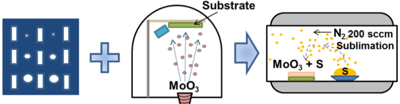
Chapter 2 A novel growth process
A novel growth process is established using MoO
3thin films as a precursor.
The process consists of four steps: MoO
3thermal evaporation, first annealing for crystallization, sulfurization and post-annealing. The main advantage of this process is originated from the first MoO
3deposition step. The use of metal shadow mask at first deposition step enabled us to pattern MoS
2thin films. In addition, changeable initial thickness of MoO
3thin films proposes possibility of MoS
2thickness control with high
Figure 2.1. Growth scheme of the MoS2 film.
21
uniformity. The crystalline structures, surface morphologies and chemical states at each step were characterized by X-ray diffraction (XRD), atomic force microscopy (AFM), Raman spectroscopy, and X-ray photoelectron spectroscopy (XPS). Based on these characterizations and a careful optimization of the growth conditions, we successfully established a novel growth process. The established growth process is outlined in Figure 2.1. In this chapter, the each process is explained.
2.1 MoO
3deposition by thermal evaporator
Before starting the experiments, substrate was considered. The substrate for experiment should be useful for device fabrication. In addition, commercialized substrate is needed because rare substrate interrupts progress of experiment. Over several decades, silicon dioxide (SiO
2), which is a typical inorganic gate insulator, has been intensively studied for application in TFTs because Si/SiO
2can be easily used as bottom gate and insulator. Consequently, it has been successfully commercialized in devices. Therefore, Si/SiO
2was used as substrate in this study. MoO
3powders, which were purchased from sigma-aldrich, were used as sources. 3 nm MoO
3thin films were deposited by thermal evaporator with rate of 0.1 Å/s for 5 minutes on Si/SiO
2substrate.
As-deposited MoO
3thin films showed flat surface as shown in Figure 2.2(a). The
crystallinity of as-deposited thin films was characterized by XRD. The substrate peak
was detected at 32.8 ° as shown in Figure 2.2(b). No diffraction peak was observed in
deposited thin films, indicating amorphous.
22
Figure 2.2. (a) AFM image and (b) XRD result measured in as-deposited MoO3 thin films.
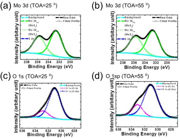
As a next step, to investigate composition of as-deposited MoO
3thin films, X-ray photoelectron spectroscopy (XPS) was measured. Take-off angles (TOA) were changed to control the detection depth in a sample. It makes possible to explore distribution of compositions. In order to survey compositions depending on change of depth in deposited MoO
3thin films, Mo 3d and O 1s spectra were measured at TOA of 25 ° (surface sensitive angle) and 55 ° (bulk sensitive angle). The results are shown in Figure 2.3. The peaks were observed at 232.7 eV for 3d
5/2, 235.7 eV for 3d
3/2in Mo 3d spectrum of TOA=25 ° and at 232.6 eV, 235.7 eV in Mo 3d spectrum of TOA=55 °.
These peaks are originated from MoO
3.
1,2To analyze composition more carefully, O 1s
spectra were also characterized as shown in Figures 2.3(c) and (d). The peaks in O 1s
spectra showed 2 peaks at 531 eV, 532.8 eV in TOA = 25 ° and 531.1 eV, 533.1 eV at
TOA = 55 °. These peaks were assigned to O-Mo bond and O-Si bond attributed from
MoO
3and SiO
2, respectively.
3,4Amount of Mo and O are judged with rate of 1:2.3 and
1:2.7 (Mo:O) at surface sensitive angle and bulk sensitive angle, respectively. This
explained that deposited MoO
3thin films have nonstoichiometric composition.
23
Furthermore, a large amount of O-deficiency was observed in surface compared with bottom side. Thus, deposited MoO
3thin films were characterized by XRD and XPS to investigate crystallinity and composition. The results demonstrated that amorphous MoO
3thin films were grown with a large amount of O-deficiency.
However, MoS
2thin films sulfureted from amorphous MoO
3was amorphous as shown in Figure 2.4(a) and (b), labeled as ‘without’. To obtain crystalline MoO
3of layered structure, which may be helpful for growing crystalline MoS
2, first annealing was carried out. In addition, O-deficiency should be avoided during the first-annealing.
Figure 2.3. XPS spectra showing chemical states of Mo and O in deposited thin films from MoO3 powder.
Chemical states of Mo at (a) surface sensitive angle (b) bulk sensitive angle and chemical states of O at (c) surface sensitive angle (d) bulk sensitive angle.
24
2.2 First annealing for MoO
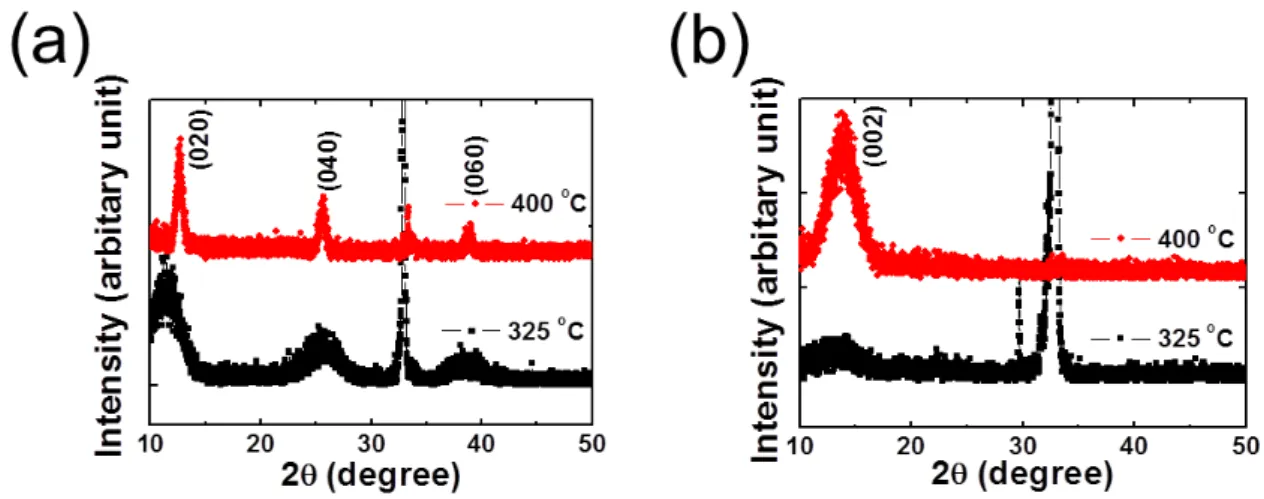
3crystallization
The first annealing was carried out under the oxygen atmosphere to obtain crystalline thin films with suppression of O-deficiency. The first annealing temperature (T
FA) was varied from 300 °C to 400 °C. The crystallinities of annealed MoO
3thin films were investigated by XRD. The films annealed at 300 °C showed no diffraction peak, while a T
FAabove 350 °C yielded periodic peaks that appeared at 12.6 °, 25.6 ° and 38.8 °, which are assigned to the (020), (040) and (060) planes,
5respectively, as shown in Figure 2.4(a). These experimental results demonstrated that the first annealing above 350 °C is effective for crystallization of MoO
3. Then, the annealed films moved to sulfurization step for formation of crystalline MoS
2.
Figure 2.4. XRD patterns of the (a) MoO3 thin films and (b) resultant MoS2 thin films. The annealing temperature (TFA) ranged from 300 °C to 400 °C. The weak and broad peak around 14.1 ° is evidence of
the MoS2 film growth.
25
2.3 Sulfurization
2.3.1 Experimental set up
The MoO
3thin films with and without first annealing needed sulfurization process for growing MoS
2thin films. In the sulfurization step, to promote the reaction between MoO
3thin films and S of vapor phase, sulfurization temperature (T
Sulf) should preferably be as high as possible. But desorption of MoO
3thin films was observed above 500 °C. Therefore, T
Sulfwas fixed at 500 °C.
On the other hand, S powders were sublimated around 113 °C. Because sublimation temperature was quite different between MoO
3and S, generally, two furnaces are used for sulfurization of MoO
3and S as shown in Figure 2.5(a). However, temperature control was difficult because too high temperature caused too fast sublimation. In addition, large distance between furnaces leads to adsorption of S to quartz tube before S atoms reach to MoO
3.
Therefore, original CVD set up was designed as seen in Figure 2.5(b). In
original CVD set up, temperature was increased to 500 °C at left side. After reaching
temperature to 500 °C, Furnace was slid to left side. Then, S powders were explosively
sublimated and reacted with MoO
3. Thus, sulfurization step was carried out with
original CVD set up.
26
Figure 2.5. (a) General CVD set up and (b) original CVD set up for sulfurization.
2.3.2 Results and discussion
MoO
3thin films were sulfurated with original CVD set up as mentioned above in Sec.2.3.1. XRD patterns of the sulfurated thin films are shown in Figure 2.4(b). No diffraction peak was observed in samples annealed at T
FAbelow 350 °C. Meanwhile, a diffraction peak was detected at samples annealed above 350 °C. The peak at 14.1 ° was assigned as the (002) plane of MoS
2.
6Furthermore, the crystallinity of MoS
2thin films depended on the crystallinity of MoO
3thin films. Thus, the crystalline MoO
3precursor film was needed to produce the crystalline MoS
2films. Because the most intensive diffraction peak was produced, T
FAwas optimized at 400 °C for the following process.
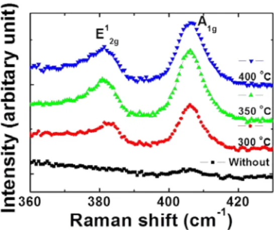
Sulfurated thin films were also characterized by Raman spectroscopy to
27
Figure 2.6. Raman spectra obtained from the sulfurated films, showing E12g and A1g modes to prove the formation of MoS2.
confirm the formation of MoS
2. Figure 2.6 shows Raman spectra, in which two peaks around 381 cm
-1and 406 cm
-1can be seen. These are the in-plane vibrational E
12gmode and the out-of-plane vibrational A
1gmode, respectively.
7-9These peaks provide clear evidence of MoS
2formation. Here, Raman peaks were observed even in films annealed at a T
FAof 300 °C, although no XRD peak was observed, indicating that a T
FAof 300 °C produced MoS
2, but the structure was amorphous.
Figure 2.7. XPS spectra of (a) Mo 3d and (b) S 2p obtained from MoS2 bulk crystal.
28
The composition of sulfurated films was investigated by XPS. For accurate analysis, bulk MoS
2crystal was measured with XPS at first. The results of XPS at bulk MoS
2crystal are shown in Figure 2.7(a) and (b). The observed peaks at 226.30 eV, 229.12 eV, 232.28 eV are assigned to S 2s, Mo 3d
5/2, Mo 3d
3/2.
1,10The S 2p spectrum showed peaks at 161.83 eV for S 2p
3/2and 163 eV for S 2p
1/2.
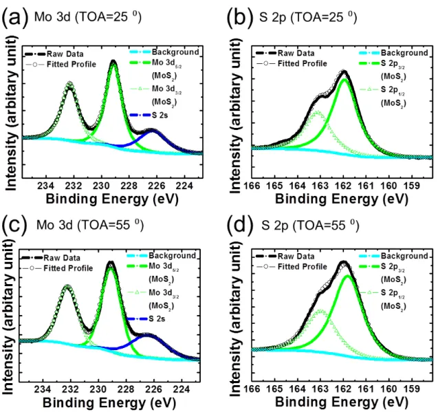
Figure 2.8. XPS spectra of (a) Mo 3d, (b) S 2p measured at TOA=25 ° and(c) Mo 3d, (d) S 2p at TOA=55 ° obtained from sulfurated thin films.
29
The chemical states of the sulfurated films at T
FA= 400 °C were examined by XPS. Figure 2.8(a) and (b) show Mo 3d and S 2p core spectra measured at TOA = 25 °, respectively. The observed peaks were calibrated with the C 1s line (284.6 eV). The Mo 3d spectrum can be divided into two components, namely, 228.75 eV for Mo 3d
5/2and 231.95 eV for Mo 3d
3/2. Another peak at 226.47 eV is from the S 2s core level. These spectra proved that molybdenum atoms were in the Mo
4+oxidation state to form MoS
2. Here, we need to take into account the fact that MoS
3also yields a similar state and it is hard to distinguish the origin of peaks because both states appear at the same bonding energies.
1,10A consistent tendency can be seen in the S 2p spectra in Figure 2.8(b). The spectra at 161.93 and 163.05 eV can be attributed to the S 2p
3/2and S 2p
1/2states of MoS
2and MoS
3. However, a careful analysis revealed that additional peaks appeared in higher bonding energy range at 163.69 eV and 164.96 eV. The respective peaks can be assigned to the S 2p
3/2and S 2p
1/2states of MoS
3, providing clear evidence of MoS
3formation.
1In the viewpoint of the charge state, MoS
3has a charge state of Mo
5+(S
22-)
1/2(S
2-)
2.
1,10It means that the S 2p spectrum have two doublets from S
22-and S
2-.
10,11The higher binding energy may be attributed to bridging S
22-ligands. The doublets with the lower energy might be attributed to terminal S
22-and/or S
2-. Because different kinds of sulfur ligands have similar binding energies in XPS, it is not possible to quantify the ratio of these sulfur ligands.
10,11Therefore, the ratio of MoS
3in grown thin film cannot be estimated.
Figure 2.8(c) and (d) show Mo 3d and S 2p spectrum measured at TOA = 55 °.
The results were similar with spectra measured at TOA = 25 °, explaining presence of
MoS
3in grown thin films. The area of observed peaks at higher binding energy, which
are originated from MoS
3, was decreased compared with those of TOA = 25 °,
30
demonstrating MoS
3existed mainly in surface of thin films.
Based on these results, we concluded that the sulfurization process produced mixed films of MoS
2and MoS
3. Therefore, post-annealing was needed to obtain MoS
2thin films without MoS
3.
2.4 Post-annealing
Sulfurated thin films were post-annealed in an Ar atmosphere. The higher post-annealing temperature (T
PA) than T
Sulfof 500 °C was needed to obtain a single component MoS
2thin film. However, T
PAof 700 °C led to desorption of thin films.
Therefore, sulfurated thin films were post-annealed at 600 °C. After the post-annealing, XPS was measured to explore that MoS
3is removed or not.
Figures 2.9(a) and (b) show Mo 3d and S 2p spectra measured at surface sensitive TOA = 25 °. In Figure 2.9(a), the XPS spectra obtained from Mo 3d fitted similarly to that in Figure 2.8(a). The observed peaks at 226.35eV, 229.16 eV, 232.28 eV were assigned to S 2s, Mo 3d
5/2, Mo 3d
3/2, respectively. Meanwhile, those from S 2p in Figure 2.9(b) were obviously affected by the post-annealing; the spectra were well fitted by just a single component peak with binding energies of 161.96 eV for S 2p
1/2and 163.17 eV for S 2p
3/2, which reveal that MoS
2was formed. No peak from MoS
3was detected in the post-annealed thin films.
Figure 2.9(c) and (d) show Mo 3d and S 2p spectra measured at TOA = 55 °.
The peaks are detected at 226.40 eV for S 2s, 229.16 eV for Mo 3d
5/2and 232.22 eV for
31
Figure 2.9. XPS spectra of (a) Mo 3d, (b) S 2p measured at TOA=25 ° and(c) Mo 3d, (d) S 2p at TOA=55 ° obtained after the post-annealing
Mo 3d
3/2. The S 2p spectrum showed clear 2 peaks, which are attributed from a single
component. The observed 2 peaks at 161.83 eV and 163 eV explained that a single
component MoS
2is grown. Thus, the XPS spectra measured at TOA = 25 ° and 55 °
explained that MoS
3was removed over the all films by post-annealing. These results
demonstrated that MoS
2thin films were successfully grown from the MoO
3precursors
with a four-step CVD method.
32
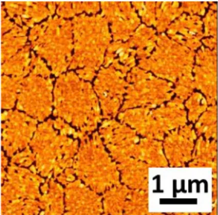
2.5 Surface morphology
To establish a novel process for MoS
2growth, various properties should be considered. The crystallinities and compositions were previously investigated by XRD and XPS, respectively. However, surface morphologies were not surveyed although surface morphology is important in device fabrication. Therefore, grown thin films were characterized by AFM for investigating surface morphology of MoS
2thin films.
Figure 2.10 shows an AFM image of grown MoS
2thin films on the Si/SiO
2substrates. An AFM image indicated a discontinuous structure with large numbers of cracks. To investigate step, which caused large numbers of cracks, we checked surface morphology of annealed MoO
3thin films.
The surface morphology of MoO
3thin films annealed at 400 °C for 2 hours is shown in Figure 2.11(a). The result indicated similar surface morphology with grown MoS
2thin films, showing large number of crack. This demonstrates that surface morphology of grown MoS
2thin films depends on surface morphology of MoO
3thin films. To improve surface morphology, the as-deposited MoO
3films were annealed at
Figure 2.10. AFM image of the MoS2 thin films grown on Si/SiO2.
33
Figure 2.11. AFM image of the MoO3 thin films after first annealing at (a) 400 °C (b) 350 °C and (c) 325 °C for 2 hours on Si/SiO2.
34
lower T
FAthan 400 °C. Figures 2.11(b) and (c) indicate surface morphologies of MoO
3thin films, which were annealed at 350 °C and 325 °C for 2 hours. The small holes were obtained in MoO
3thin films annealed at 350 °C, indicating a discontinuous structure.
Meanwhile, MoO
3thin films annealed at 325 °C revealed continuous MoO
3thin films.
Thus, MoS
2thin films at T
FA= 325 °C satisfied the requirement of smooth morphology.
Therefore, we conclude that the T
FAof 325 °C is more appropriate than T
FAof 400 °C for growing MoS
2in terms of surface morphology.
However, here, we should consider crystallinity as well as surface morphology of grown MoS
2because crystallinity is also important factor to obtain high performance transistor. Furthermore, as mentioned in Sec. 2.3, because low first annealing temperature caused low crystallinity MoS
2thin films, crystallinity at T
FA= 325 °C should be investigated. For example, the MoS
2sample at T
FA= 350 °C showed lower crystallinity than sample at T
FA= 400 °C as shown in Figure 2.5. Moreover, T
FA= 300 °C caused amorphous MoS
2thin films. Therefore, the crystallinities of MoO
3and MoS
2at T
FA= 325 °C are investigated by XRD. As shown in Figure 2.12(a),
MoO
3thin films was crystallized at T
FA= 325 °C. However, crystallinity of MoO
3at
T
FA= 325 °C was much lower than those of at T
FA= 400 °C. In addition, grown MoS
2thin films from MoO
3at T
FA= 325 °C indicated decreased crystallinity compared with
those at T
FA= 400 °C as shown in Figure 2.12(b). It means that grown thin films at T
FAof 325 °C is not appropriate as channel layers in terms of crystallinity although smooth
surface was obtained.
35
Figure 2.12. XRD results of (a)MoO3 thin films at TFA = 325 °C, 400 °C and (b)subsequently grown MoS2.
Thus, two requirements of smooth surface morphology and high crystallinity were not satisfied by changing first annealing temperature. Therefore, to satisfy two requirements at same time, additional method was considered to improve crystallinity of grown MoS
2thin films. At this time, first annealing temperature was kept at T
FA= 325 °C, which shows smooth surface morphology.
Because cracks are caused by difference of thermal expansion coefficient, the
problem is expected as difference of thermal expansion coefficient between substrate
and MoO
3. As a method to improve the crystallinity with fixed T
FAof 325 °C, change of
substrate was considered. Among a large number of substrates, sapphire substrate has
closer thermal expansion coefficient (4.5×10
-6/K) with that of MoO
3(9×10
-6/K) than
SiO
2(5×10
-7/K). Moreover, c-plane sapphire substrate shares some symmetry with the
MoS
2structure.
12It has been shown previously that under similar conditions, the use of
an sapphire substrate led to significantly better quality of MoS
2.
13-17Therefore, sapphire
substrate with an atomically flat surface was explored instead of Si/SiO
2substrate.
36
Figure 2.13. (a) XRD patterns of the MoS2 films grown on the Si/SiO2 (black line) and sapphire (red line) substrates. The inset shows rocking curves on the respective substrates.
Figure 2.13(a) showed XRD results, which were measured in grown MoS
2thin films on Si/SiO
2and c-plan sapphire substrates. The weak diffraction peak at 13.9 ° observed on the Si/SiO
2substrate was much larger than on the sapphire. Furthermore, grown MoS
2thin films on sapphire substrate showed sharp peak in the rocking curve with a full-width at half-maximum (FWHM) of 0.11 °. This is clear proof of a high orientation along the c-axis as indicated in Figure 2.13(a) inset; two-dimensional MoS
2atomic layers were parallel to the sapphire substrate. Meanwhile, the rocking curve obtained from the Si/SiO
2substrate showed no signal. I suggest the film on the Si/SiO
2substrate had a polycrystalline and/or amorphous structure with a marginal c-axis orientation.
These results explain that sapphire substrate improved the crystallinity of the MoS
2films. In addition, the AFM image in Figure 2.13(b) shows the surface morphology of a
MoS
2film grown on a sapphire substrate. The resultant film had a continuous and flat
structure with root-mean-square surface roughness of 0.3 nm. Such a continuous and
37
flat surface was observed over the complete substrate. The inset is a photograph of thus prepared MoS
2film. The method ensures full coverage of the centimeter-square surface.
2.6 Conclusion
In conclusion, a multi-step CVD process was established for growing highly oriented MoS
2films. The first step consisting of MoO
3thermal evaporation was essential for obtaining controllability and uniformity of the thickness, and for location control of MoS
2. The second step, consisting of thermal annealing in oxygen, produced crystalline MoO
3thin films with a layered structure, which were strongly required for the subsequent third step of sulfurization. Although the films after the sulfurization process consisted of a polycrystalline and amorphous mixture of MoS
2and MoS
3, the fourth step, namely the post-annealing in Ar, yielded single-component layered MoS
2films. Other important requirements are smooth surface morphology and high
crystallinity for high performance transistor, which will discuss in next chapter. For
these purposes, first annealing temperature and substrate are carefully investigated. A
continuous structure, flat surface, excellent thickness uniformity and high c-axis
orientation of the MoS
2films were achieved on a centimeter square c-plan sapphire
substrate. Importantly, I would like to emphasize that position-selective film growth is
available by using shadow masks in the first deposition process. This advantage opens
the possibility of producing functional devices with simple techniques.
38
References
1
L. Benoista, D. Gonbeaua, G. Pfister-Guillouzoa, E. Schmidtb, G. Meunierb and A.
Levasseurb, Thin Solid Films 258, 110 (1995).
2
R. Benjaram M, C. Biswajit, R. Ettireddy P, F. Asunción, Applied Catalysis A 213, 279 (2001).
3
T. H. Fleisch and G. J. Mains, J. Chem. Phys. 76, 780 (1982).
4
E. J. D. Klem, H. Shukla, S. Hinds, D. D. MacNeil, L. Levina and E. H. Sargent, Appl.
Phys. Lett. 92, 212105 (2008).
5
J. Torres, J. E Alfonso, and L. D. López-Carreño, phys. stat. sol. (c) 2, 3726 (2005).
6
G. Alexander S, B. Ivan S, L. Natalia D, B. Mikhail I, G. Alexandre S, and A. Mikhail Yu, J. Phys. Chem. C 117, 8509 (2013).
7
C. Lee, H. Tan, L. E. Brus, T. F. Heinz, J. Hone and S. Ryu, ACS Nano 4, 2695 (2010).
8
K. Gołasa, M. Grzeszczyk, R. Boż ek, P. Leszczyński, A. Wysmołek, M. Potemski and A. Babiński, Solid State Communications 197, 53 (2014).
9
H. Li, Q. Zhang, R. C. C. Yap, B. K. Tay, T. H. T. Edwin, A. Olivier and D.
Baillargeat, Adv. Funct. Mater. 22, 1385 (2012).
10
T. Weber, J. C. Masers and J. W. Niemantsverdriet, J. Phys. Chem. 99, 9194 (1995).
11
H. Vrubel, D. Merki and X. Hu, Energy Environ. Sci. 5, 6136 (2012).
12
L. Ma, D. N. Nath, E. W. Lee II, C. H. Lee, M. Yu, A. Arehart, S. Rajan and Y. Wu, Appl. Phys. Lett. 105, 072105 (2014).
13
Q. Q. Ji, Y. F. Zhang, T. Gao, Y. Zhang, D. L. Ma, M. X. Liu, Y. B. Chen, X. F. Qiao, P. H. Tan, M. Kan, J. Feng, Q. Sun and Z. F. Liu, Nano Lett. 13, 3870 (2013).
14
Y. M. Shi, W. Zhou, A. Y. Lu, W. J. Fang, Y. H. Lee, A. L. Hsu, S. M. Kim, K. K.
39
Kim, H. Y. Yang, L. J. Li, J. C. Idrobo and J. Kong, Nano Lett. 12, 2784 (2012).
15
A. Koma and K. Yoshimura, Surf. Sci. 174, 556 (1986).
16
K. Ueno, K. Saiki, T. Shimada and A. Koma, J. Vac. Sci. Technol. A 8, 68 (1990).
17
F. S. Ohuchi, T. Shimada, B. A. Parkinson, K. Ueno and A. Koma, J. Cryst. Growth
111, 1033 (1991).
40
Chapter 3 Field effect transistor (FET) application of MoS 2 thin films
MoS
2transistors were fabricated with thin films grown by a multi-step CVD process. I found that the MoS
2transistor properties were greatly affected by the post-annealing temperature (T
PA). The films worked as ambipolar transistors below T
PA=1000 °C. Meanwhile, the transistor operation transited from ambipolar to n-type transport at a T
PAof 1000 °C. X-ray photoelectron spectroscopy (XPS) measurements revealed that the films annealed below 1000 °C had sulfur-rich compositions (S/Mo > 2).
The excess S atoms were reduced by elevating the annealing temperature to produce almost stoichiometric composition (S/Mo = 2) at 1000 °C. These results indicate that excess sulfurs are responsible for the ambipolar operation by acting as acceptors that generate holes. Moreover, the high-temperature annealing at 1000 °C had another distinct effect, i.e., it improved the crystallinity of the MoS
2films. The electron mobility consequently reached 0.20±0.12 cm
2/V∙s.
3.1 Principle of FET
3.1.1 Operation
General thin film transistor consists of semiconductor layer and three
electrodes (source, drain and gate). One of the three electrodes is separated from the
41
semiconductor by a thin gate-insulator (gate electrode). The semiconductor between the source and the drain below the gate electrode forms the channel, defined by the channel width (W) and the channel length (L). The source to drain current flows via a conducting channel. At this time, kind of charge carriers, which flow between source and drain, is determined by material (P-type or N-type semiconductor). In P-type material, electric charges are carried mainly in the form of electron deficiencies called holes. In N-type material, the charge carriers are primarily electrons. This flowing current is controlled by electric field that is produced when a voltage is applied between the gate and source terminals. The schematic illustration of the N-type transistor is shown in Figure 3.1.
The operation of an N-type transistor can be described as follows. For example, n-type material, the minimum gate to source voltage differential, which is needed to create a conducting path, is defined as threshold voltage (V
th). When gate-source voltage (V
GS) ≤ V
th, current nearly not flows through source to drain. In this region,
"off" current is extracted, which needs for calculation of on/off ratio.
When V
GSis higher than V
thwith positive voltage drain-source voltage (V
DS), electrons from source region enter the channel and reach the drain. If V
DSis increased, current flowing through the channel is increased. In this region, plot of drain-source current (I
DS) versus V
DSis a straight line as shown in Figure 3.1(a). Here, the slope of I
DSversus V
DSline is the conductance of the channel. To control applied V
GSchanges its n-type charge concentration. Therefore, change of V
GSaffects to conductance, which extracts from the slope of I
DSversus V
DSline. In this region, drain current in given by the following equation.
1I
DS= ((W∙C
i∙μ)/2L) (V
GS-V
th)
2(3.1)
42